background image

6-3

(5-4) ARP to RAM Address Bus

Data write 

 other address read discord check

Error 10: ARP 

 RAM address bus error

Caution: Address and data display in case of an error is

different from the display of other diagnosis (de-
scribed later).

Before starting the test, all addresses of RAM (IC304) are
cleared to 0x0000.
First, 0xA55A is written to the address 0x00000, and the
address data are read and checked from addresses 0x00001
to 0x80000 while shifting 1 bit each. Next, the data at that
address is cleared, and it is written to the address 0x00001,
and read and checked in the same manner. This check is
repeated up to the address 0x80000 while shifting the ad-
dress data by 1 bit each.
If data other than 0 is read at the addresses except written
address, an error is given because all addresses were al-
ready cleared to 0. In this check, the error display pattern is
different from that of other diagnosis; read data, written
address, and read address are displayed in this order. How-
ever, the message uses same template, and accordingly ex-
change Address and Data when reading. The following dis-
play, for example,

### Syscon Diagnosis ###

 5-4. ARP to RAM Address Bus

Error 10: ARP - RAM Address B

Address

: 0000A55A

Write Data : 00000000

Read Data

: 00080000

Press NEXT Key to Continue

Press PREV Key to Repeat

_

shows the data 0xA55A was read from address 0x00080000
though it was written to the address 0x00000000. This im-
plies that these addresses are in the form of shadow. Also,
if the read data is not 0xA55A, another error will be present.

(5-5) ARP RAM Check

Data write 

 read, and accord check

Error 11: ARP RAM read data discord
The program code data stored in ROM are copied to all
areas of RAM (IC304) connected to the ARP (IC303)
through the bus, then they are read and checked if they ac-
cord. If the detail check was selected initially, the data are
written to all areas and read, then the same test is conducted
once again with the data where all bits are inverted between
1 and 0. If discord is detected, faulty address, written data,
and read data are displayed following the error code 11,
and the test is suspended.

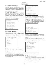
6.

AV Decoder

(6-2) 1930 RAM

Data write 

 read, and accord check

Error 13: AVD RAM read data discord
The program code data stored in ROM (IC206) are copied
to all areas of RAM (IC402, IC403) connected to the AVD
(IC401) through the bus, then they are read and checked if
they accord. Further, the same test is conducted once again
with the data where all bits are inverted between 1 and 0. If
discord is detected, faulty address, written data, and read
data are displayed following the error code 13, and the test
is suspended.

(6-3) 1930 SP

ROM 

 AVD RAM 

 Video OUT

Error: Not detected.
The data including sub picture streams in ROM (IC206)
are transferred to the RAM (IC402, IC403) in AVD (IC401),
and output as video signals from the AVD (IC401).
They are output from all video terminals (Composite, Y/C,
Component) except EURO AV terminal.

7.

Video

(7-2) Color Bar

AVD color bar command write 

 Video OUT

Error: Not detected.
The command is transferred to the AVD, and the color bar
signals are output from video terminals.
They are output from all video terminals (Composite, Y/C,
Component) except EURO AV terminal.

8.

Audio

(8-2) ARP 

 1930

Error 14: ARP 

 1930 video NG

         15 : ARP 

 1930 audio NG

(8-3) Test Tone

A pink noise signal is output from the AVD (IC401) through
optical coaxial digital terminal and analog audio terminal.
Error: Not detected.
All channels 

 2ch Left 

 2ch Right 

 Front Left 

Front Right 

 Rear Left 

 Rear Right 

 Center 

 Sub

Woofer are checked in this order.
Caution: Sub Woofer is checked only for low-frequency

components, and no sound will be heard unless a
proper super woofer is connected.

Summary of Contents for DVP-S533

Page 1: ...ive S VIDEO OUT 4 pin Y 1 0 Vp p 75 ohms 1 2 mini DIN sync negative C 0 286 Vp p 75 ohms terminated COMPONENT phono Y 1 0 Vp p 75 ohms VIDEO OUT jacks sync negative Y PB B Y PB B Y PR R Y PR R Y 0 7 Vp p 75 ohms PHONES Phone 12 mW 32 ohms jack 5 1CH Phono 2 Vrms Over 10 kilohms OUTPUT jacks at 50 kilohms General Power requirements 110 to 240 V AC 50 60 Hz Power consumption 16 W Dimensions approx 4...

Page 2: ... product will increase eye hazard 1 Check the area of your repair for unsoldered or poorly sol dered connections Check the entire board surface for solder splashes and bridges 2 Check the interboard wiring to ensure that no wires are pinched or contact high wattage resistors 3 Look for unauthorized replacement parts particularly transis tors that were installed during a previous repair Point them ...

Page 3: ...ram 4 33 MB 85 DAC Schematic Diagram 4 35 MB 85 BIAS Schematic Diagram 4 37 AU 212 AUDIO VIDEO BUFFER Printed Wiring Board 4 39 AU 212 AUDIO Schematic Diagram 4 41 AU 212 VIDEO BUFFER Schematic Diagram 4 43 FL 101 FUNCTION SWITCH IF CON Printed Wiring Board 4 45 FL 101 FUNCTION SWITCH Schematic Diagram 4 47 FL 101 IF CON Schematic Diagram 4 49 HP 111 HEADPHONE Printed Wiring Board and Schematic Di...

Page 4: ... shown below Set Case Page 2 1 Power Block Page 2 1 AU 212 Board Page 2 1 Mechanism Deck Page 2 2 Front Panel Page 2 2 Tray Cover Page 2 2 Optical Pick up Page 2 3 TK 51 Board Page 2 3 Belt Page 2 3 Loading Motor M001 MS 46 Board Page 2 3 Tray Page 2 2 MB 85 Board Page 2 1 ...

Page 5: ...s See Fig 1 2 Open the side of case See Fig 1 3 Remove the case as lift straight See Fig 1 Fig 1 3 DISC REMOVAL PROCEDURE at POWER OFF 1 Insert a tapering driver into the aperture of the unit bottom and move the lever of chuck cam in the direction of the arrow A See Fig 2 2 Draw out the tray in the direction of the arrow B and remove a disc See Fig 2 Fig 2 Two screws Three screws Case Two screws L...

Page 6: ...1 1 SECTION 1 GENERAL This section is extracted from in struction manual 3 867 038 11 DVP S533D ...

Page 7: ...1 2 ...

Page 8: ...1 3 ...

Page 9: ...1 4 ...

Page 10: ...1 5 ...

Page 11: ...1 6 ...

Page 12: ...1 7 ...

Page 13: ...1 8 ...

Page 14: ...1 9 ...

Page 15: ...1 10 ...

Page 16: ...1 11 ...

Page 17: ...1 12 ...

Page 18: ...1 13 ...

Page 19: ...1 14 1 14 E ...

Page 20: ...wo screws 1 Three screws 4 Two flat cables CN004 007 2 Two flat cables CN002 003 6 Flat cable CN006 8 MB 85 board 7 Four screws B3 3 Connector CN001 1 Connector CN011 5 Flat cable CN005 1 Connector CN101 2 Three connectors CN201 202 203 3 Four screws B3 4 Power block 7 Three screws B3 5 Four screws B3 6 Four screws B3 2 Connector CN401 1 Connector CN201 3 Two flat cables CN302 303 4 Flat cable CN3...

Page 21: ...move the lever of chuck cam in the direction of the arrow A 3 Two claws B A 4 Screw B3 2 Connector CN701 3 Flat cable CN006 1 Connector CN203 5 Two screws B3 9 Claw 8 Claw º Front panel 6 Boss 7 Boss 2 Two flat cables CN003 004 3 Screw B3 4 Mechanism deck 1 Connector CN001 2 Chuck ass y 4 Remove the tray in the direction of the arrow B 3 Move the lever of chuck cam in the direction of the arrow A ...

Page 22: ...Remove the base unit holder in the direction of the arrow A 2 Two claws 1 Two flexible board CN001 002 5 Optical pick up 4 Three step screws A 2 Two screws B2 6 4 1 Belt 9 TK 51 board 8 Claw 7 Claw 6 Flexible board CN001 5 Flexible board CN002 3 Three claws 4 Loading motor M001 MS 46 board ...

Page 23: ...2 4 2 11 INTERNAL VIEW DC motor loading 1 541 632 11 Optical pick up KHM 220AAA J1RP 8 820 081 03 ...

Page 24: ...IRCUIT BOARDS LOCATION Power Block HS 030SF SWITCHING REGULATOR TK 51 RF SERVO AU 212 AUDIO MB 85 SIGNAL PROCESS SERVO FL 101 FUNCTION SWITCH MS 46 LOADING SW 317 SURROUND SWITCH HP 111 HEADPHONE FR 150 IR POWER SWITCH ...

Page 25: ...1 HGA Serial BUS JOG UNIT SW REG 12V EVER5V 3 3V 5V A 12V M 12V 3 3V 5V 12V 12V EVER5V SWITCH SWITCH SWITCH ND201 IC201 IF CON IC203 S LINK IC701 IC202 IC802 SPINDLE SLED LOADING MOTOR DRIVE CDDOUT CDDATA CDBCK CDLRCK IC303 ARP2 SD 0 7 RF IC401 AV DECODER IC304 16M DRAM IC402 403 16M SDRAM IC204 1M SRAM IC201 4K EEP ROM IC206 16M FLASH IC902 AUDIO 2CH DAC SPDIF Parallel BUS VIDEO V VIDEO Y VIDEO C...

Page 26: ...KIN 50 26 108 GIO 0 GIO 5 8 DAB 0 1 DAB 2 3 GIO 1 2 PWM 0 2 TRD TILT MUTE FGMODE FCD TLTA TLTB 117 ı 120 122 ı 125 74 81 84 93 96 15 ı 18 13 14 2 3 23 26 FOCUS COIL DRIVE TILT MOTOR DRIVE Q802 803 GAIN CONTROL TRD FCD TLTA TLTB 7 9 20 IC801 IC701 IC702 1 2 11 ı 14 15 16 17 18 SPINDLE MOTOR DRIVE LOADING MOTOR DRIVE SLED MOTOR DRIVE SLDA SLDB STVC 3 3V 2 5VC 2VC 1 6VC 5V 20 26 23 IC802 3 1 IC702 2 ...

Page 27: ...5 118 120 123 125 127 129 132 148 150 152 63 68 70 71 HA 0 21 HD 0 15 IC402 403 16M SDRAM DDT 0 15 DAD 0 11 107 ı 110 29 ı 32 47 ı 51 91 93 ı 96 97 98 100 ı 105 SD 0 7 SD 0 7 DT 0 7 I SDCK SDEF XSHD XSAK XSRQ CDDOUT CDDATA CDBCK CDLRCK CDDOUT CDDATA CDBCK CDLRCK 38 ı 43 45 46 166 167 193 194 196 198 ı 202 168 170 172 178 180 187 189 192 2 5 7 10 12 15 205 208 21 22 23 ACH12 ACH34 ACH56 LRCK BCK CD...

Page 28: ...XFRRST XIFINT LDMP DMP LDMM DMM OCSW1 OCSW2 CKSW1 FCSON SPDLSTOP SPGAIN XDRVMUTE LDMP DMP LDMM DMM OCSW1 OCSW2 CKSW1 94 93 92 91 64 63 88 X01INT0 X01INT1 X01CS 29 30 28 XDACS2 XDACS3 X01RST XDACRST MA MUTE 96 97 XDACS2 XDACS3 MA MUTE 31 26 49 126 133 146 154 PLL IC001 IC003 IC004 N27MHGA RF SERVO SEE PAGE 3 4 SIGNAL PROCESS VIDEO SEE PAGE 3 5 AUDIO 2 SEE PAGE 3 11 AUDIO 2 SEE PAGE 3 11 RST PB7 PB3...

Page 29: ...TB CLK ACKI RST 3 1 2 26 16 13 21 17 27 28 5 22 IC906 REAR L R DAC V OUT L V OUT R ZERO ZEROR BCLKIN LRCIN D IN MD AUDIOLS AUDIORS ZFLS ZFRS MC ML SO1 SC1 CS2 XTI RSTB 3 1 2 26 16 13 21 17 27 28 5 22 IC907 CENTER WOOFER DAC V OUT L V OUT R ZERO ZEROR BCLKIN LRCIN D IN MD AUDIOC AUDIOLFE ZFC ZFLFE MC ML SO1 SC1 CS3 SO1 SC1 SO1 SC1 CS0 CS1 CS2 CS3 SO1 SC1 XDACS0 XDACS1 XDACS2 XDACS3 CDDOUT CDDATA CD...

Page 30: ... 304 MUTE CONTROL 3 1 3 1 DIGITAL OUT Q341 BUFFER D IN IC431 IC502 IC541 IC571 IC401 IC505 LEVEL L FRONT HPR HPL CN701 CN401 J508 J505 J502 R L AUDIO OUT1 OPTICAL COAXIAL R L AUDIO OUT2 R L REAR 5 1CH OUTPUT R CENTER WOOFER PHONES J701 HP 111 BOARD SEE PAGE 4 51 CN005 CN301 A MUTE MA MUTE AUDIORS ZFLS 05 ZFRS GAIN2 CN007 CN302 AUDIOLS AUDIORS ZFLS ZFRS AUDIOLS A MUTE MA MUTE GAIN2 SPDIF AUDIOLT AU...

Page 31: ...E X201 4MHz SCLK1 SOUT1 SIN1 SBUSY1 SRDY1 FRRST N V MUTE A MUTE N X IN L JOG L MULTI X OUT IFSC0 SYSTEM CONTROL SEE PAGE 3 8 SIGNAL PROCESS VIDEO SEE PAGE 3 5 AUDIO 2 SEE PAGE 3 11 IFSI0 IFSO0 XVIFCS XIFINT XFRRST V MUTE A MUTE 6 4 5 3 2 8 9 1 10 6 4 5 3 2 15 15 8 9 1 4 CN201 6 7 2 3 1 70 6 9 7 31 32 71 72 76 78 29 30 8 11 12 77 10 27 4 AN1 AN0 5 STATUS N 3 3V 3 3V 5V SHUFFLE S224 PROGRAM S223 CLE...

Page 32: ...T CN202 9 12 3 3V PCONT 05 10 5 8 CN002 9 12 10 5 Q201 30V REG IC202 IC203 ND201 Q001 002 T001 DC DC CONVERTER IC201 IC051 15 CN099 EVER5V EVER5V 1 CN003 PCONT EVER5V 12V 1 15 CN001 5 1 2 4 B301 12V 12V 5V EVER5V 3 3V 6 1 2 7 5 CN001 5V 3 3V V3 3V CN006 A 12V A 5V S12V 3 3V A 12V M 12V 5V 3 3V 2 1 IC301 9V REG IC302 9V REG IC303 IC321 IC505 EVER5V 3 3V IC404 3 3 REG IC904 A 5V REG IC801 IC802 IC40...

Page 33: ...V or less are not indicated except for electrolytics and tantalums All variable and adjustable resistors have characteristic curve B unless otherwise noted 2 nonflammable resistor 5 fusible resistor C panel designation internal component C adjustment for repair U B Line V B Line Circled numbers refer to waveforms Voltages are dc between measurement point Readings are taken with a color bar signals...

Page 34: ...DVP S533D 4 3 4 4 4 1 FRAME SCHEMATIC DIAGRAM FRAME 1 SCHEMATIC DIAGRAM FRAME 1 2 ...

Page 35: ...DVP S533D FRAME 2 SCHEMATIC DIAGRAM 4 5 4 6 FRAME 2 2 ...

Page 36: ...B 2 IC001 C 1 Q001 A 2 Q002 D 1 There are few cases that the part isn t mounted in this model is printed on this diagram RF SERVO TK 51 Power Block HS 030SF SWITCHING REGULATOR TK 51 RF SERVO AU 212 AUDIO MB 85 SIGNAL PROCESS SERVO FL 101 FUNCTION SWITCH MS 46 LOADING SW 317 SURROUND SWITCH HP 111 HEADPHONE FR 150 IR POWER SWITCH CN003 1 672 677 12 TK 51 BOARD SIDE A 12 A B C D 1 2 3 05 C E B C E ...

Page 37: ... 200 mV DIV 500 ms DIV 592 mVp p 4 IC001 ª CD play 200 mV DIV 20 ms DIV 448 mVp p 5 IC001 ª DVD play 500 mV DIV 50 ms DIV 1 3 Vp p 6 IC001 ª CD play 500 mV DIV 200 ms DIV 1 7 Vp p 7 IC001 º DVD play 100 mV DIV 50 ms DIV 180 mVp p 8 IC001 º CD play 500 mV DIV 50 ms DIV 860 mVp p 9 IC001 DVD play 500 mV DIV 100 ns DIV 1 5 Vp p º IC001 CD play 500 mV DIV 500 ns DIV 1 5 Vp p RF SERVO TK 51 ...

Page 38: ...IAGRAM See page 4 7 for printed wiring board and page 4 10 for waveforms Ref No TK 51 board 2 000 series RF SERVO TK 51 Note The components identified by mark or dotted line with mark are critical for safety Replace only with part number specified ...

Page 39: ... t mounted in this model is printed on this diagram LOADING MS 46 05 1 675 146 11 MS 46 BOARD 11 CHUCK SENSOR LOADING MOTOR S001 TRAY SENSOR CN001 S001 Power Block HS 030SF SWITCHING REGULATOR TK 51 RF SERVO AU 212 AUDIO MB 85 SIGNAL PROCESS SERVO FL 101 FUNCTION SWITCH MS 46 LOADING SW 317 SURROUND SWITCH HP 111 HEADPHONE FR 150 IR POWER SWITCH ...

Page 40: ...ef No MB 85 board 1 000 series MB 85 BOARD SIDE A CN001 D 2 CN002 D 4 CN003 D 5 CN004 C 1 CN005 B 1 CN006 C 7 CN007 C 1 CN010 B 6 CN011 D 6 CN012 D 6 D801 C 6 D802 C 6 D803 C 6 D804 C 6 D805 C 5 D807 C 5 IC001 A 2 IC003 A 3 IC004 B 3 IC202 A 5 IC206 B 6 IC302 D 3 IC303 C 4 IC401 C 2 IC501 A 2 IC601 A 4 IC701 C 5 IC904 A 1 Q801 C 5 Q802 C 6 Q803 C 6 There are few cases that the part isn t mounted i...

Page 41: ... PROCESS SERVO MB 85 MB 85 BOARD SIDE B D701 C 2 D806 C 2 IC005 A 6 IC201 A 3 IC203 A 3 IC204 B 2 IC207 A 2 IC304 C 3 IC402 C 5 IC403 C 5 IC404 D 5 IC702 B 1 IC801 C 2 IC802 C 1 IC803 C 1 IC902 A 6 IC905 B 6 IC906 B 6 IC907 C 6 ...

Page 42: ...DVP S533D 4 19 4 20 MB 85 AV DECODER SCHEMATIC DIAGRAM See page 4 15 for printed wiring board Ref No MB 85 board 1 000 series AV DECODER MB 85 1 10 ...

Page 43: ... SCHEMATIC DIAGRAM See page 4 15 for printed wiring board Ref No MB 85 board 1 000 series SDRAM MB 85 2 10 Waveforms 1 IC401 720 mVp p H 2 IC401 728 mVp p H 3 IC401 1 0 Vp p H 4 IC401 1 1 Vp p H 5 IC401 816 mVp p H 6 IC401 1 2 Vp p H ...

Page 44: ...printed wiring board Ref No MB 85 board 1 000 series SERVO DSP MB 85 3 10 Waveforms 1 IC701 ª DVD play 500 mV DIV 50 ms DIV 1 4 Vp p 2 IC701 ª CD play 500 mV DIV 200 mV DIV 1 7 Vp p 3 IC701 DVD play 100 mV DIV 5 ms DIV 180 mVp p 4IC701 CD play 500 mV DIV 50 ms DIV 860 mVp p ...

Page 45: ...DVP S533D 4 25 4 26 MB 85 DRIVE SCHEMATIC DIAGRAM See page 4 15 for printed wiring board Ref No MB 85 board 1 000 series DRIVE MB 85 4 10 ...

Page 46: ... MB 85 ARP SCHEMATIC DIAGRAM See page 4 15 for printed wiring board Ref No MB 85 board 1 000 series ARP MB 85 5 10 Waveforms 1 IC303 DVD play 500 mV DIV 100 ns DIV 1 6 Vp p 2 IC303 ª CD play 500 mV DIV 200 ns DIV 1 6 Vp p ...

Page 47: ...D 4 29 4 30 SYSTEM CONTROL MB 85 6 10 MB 85 SYSTEM CONTROL SCHEMATIC DIAGRAM See page 4 15 for printed wiring board Ref No MB 85 board 1 000 series Waveforms 1 IC202 2 4 Vp p 12 5 MHz 2 IC202 5 4 Vp p 25 3 MHz ...

Page 48: ...DVP S533D 4 31 4 32 MB 85 HGA SCHEMATIC DIAGRAM See page 4 15 for printed wiring board Ref No MB 85 board 1 000 series HGA MB 85 7 10 ...

Page 49: ... CD 5 Vp p 33 6 MHz 3 IC001 6 4 2 Vp p 27 0 MHz 4 IC001 4 6 Vp p 33 8 MHz 6IC001 DVD play 4 2 Vp p 25 3 MHz 7 IC001 CD play 4 7 Vp p 22 5 MHz 5 IC001 DVD 5 8 Vp p 36 5 MHz CD 5 1 Vp p 33 8 MHz Waveforms MB 85 CLOCK GENERATOR AUDIO DSP SCHEMATIC DIAGRAM See page 4 15 for printed wiring board Ref No MB 85 board 1 000 series ...

Page 50: ...DVP S533D 4 35 4 36 MB 85 DAC SCHEMATIC DIAGRAM See page 4 15 for printed wiring board Ref No MB 85 board 1 000 series DAC MB 85 9 10 ...

Page 51: ...DVP S533D 4 37 4 38 MB 85 BIAS SCHEMATIC DIAGRAM See page 4 15 for printed wiring board Ref No MB 85 board 1 000 series BIAS MB 85 10 10 ...

Page 52: ... 11 IC301 C 11 IC302 A 11 IC303 B 6 IC321 B 3 IC401 B 5 IC431 B 7 IC502 B 8 IC505 A 1 IC541 B 9 IC571 B 10 Q301 B 4 Q303 A 11 Q304 C 2 Q305 C 6 Q306 C 9 Q307 C 7 Q308 C 9 Q309 C 10 Q310 C 10 Q311 C 10 Q314 B 3 Q315 B 3 Q321 B 3 Q322 A 3 Q341 A 1 Q401 B 6 Q402 B 6 Q431 B 7 Q432 C 7 Q435 C 6 Q436 A 8 Q503 B 9 Q504 A 8 Q543 B 10 Q544 A 9 Q573 B 11 Q574 A 10 AUDIO VIDEO BUFFER AU 212 Power Block HS 03...

Page 53: ...DVP S533D 4 41 4 42 AU 212 AUDIO SCHEMATIC DIAGRAM Ref No AU 212 board 2 000 series AUDIO AU 212 1 2 ...

Page 54: ...HEMATIC DIAGRAM See page 4 39 for printed wiring board Ref No AU 212 board 2 000 series VIDEO BUFFER AU 212 2 2 Waveforms 1 IC321 2 1 1 Vp p H 2 IC321 4 1 2 Vp p H 3 IC321 7 860 mVp p H 4 IC321 º 1 8 Vp p H 5 IC321 2 4 Vp p H 6 IC321 2 0 Vp p H ...

Page 55: ...204 C 13 D205 B 12 D206 B 1 D207 B 1 IC201 B 9 IC202 A 10 IC203 B 12 Q201 B 1 1 672 238 12 FL 101 BOARD 12 A B C 1 2 3 4 5 6 7 8 9 10 11 12 13 PROGRAM SHUFFLE D203 DOLBY DIGITAL FLUORESCENT INDICATOR TUBE CLEAR REPEAT OPEN CLOSE 1 3 4 5 17 PREV NEXT 1 TITLE DVD MENU RETURN JOG D204 S208 1 9 05 Power Block HS 030SF SWITCHING REGULATOR TK 51 RF SERVO AU 212 AUDIO MB 85 SIGNAL PROCESS SERVO FL 101 FU...

Page 56: ...DVP S533D 4 47 4 48 FL 101 FUNCTION SWITCH SCHEMATIC DIAGRAM See pages 4 45 for printed wiring board Ref No FL 101 board 2 000 series FUNCTION SWITCH FL 101 1 2 ...

Page 57: ...DVP S533D 4 49 4 50 Waveform 1 IC201 3 9 Vp p 4 MHz IF CON FL 101 2 2 FL 101 IF CON SCHEMATIC DIAGRAM See pages 4 45 for printed wiring board Ref No FL 101 board 2 000 series ...

Page 58: ...317 SURROUND SWITCH FR 150 IR POWER SWITCH PRINTED WIRING BOARDS Ref No SW 317 board and FR 150 board 4 000 series 05 1 672 239 12 FR 150 BOARD 12 ON STANDBY 3 2 1 A B 1 2 3 4 FR 150 BOARD CN001 B 3 CN002 A 5 CN003 A 2 D001 A 4 D002 A 4 D003 B 4 D004 A 4 D071 A 1 IC051 A 1 Q001 A 3 Q002 A 3 Power Block HS 030SF SWITCHING REGULATOR TK 51 RF SERVO AU 212 AUDIO MB 85 SIGNAL PROCESS SERVO FL 101 FUNCT...

Page 59: ...DVP S533D 4 53 4 54 SW 317 SURROUND SWITCH FR 150 IR POWER SWITCH SCHEMATIC DIAGRAM Ref No SW 317 board and FR 150 board 4 000 series SURROUND SWITCH IR POWER SWITCH SW 317 FR 150 ...

Page 60: ... D185 C 3 D211 B 1 D212 B 2 D311 A 2 D401 C 1 D402 C 1 D511 B 2 D611 B 2 IC301 A 2 IC401 C 1 Q101 B 3 Q102 A 3 Q103 B 3 Q131 A 2 Q181 C 2 Q182 C 3 Q183 C 2 SWITCHING REGULATOR HS 030SF There are few cases that the part isn t mounted in this model is printed on this diagram Power Block HS 030SF SWITCHING REGULATOR TK 51 RF SERVO AU 212 AUDIO MB 85 SIGNAL PROCESS SERVO FL 101 FUNCTION SWITCH MS 46 L...

Page 61: ...R114 2 2k D105 1SS270A PC103 TLP721F PC101 TLP721F IC401 AN1431T R402 1k C402 1uF 50V R403 1 2k R404 270 R405 1 5k R401 68 D401 11EQS04 C401 100uF 35V D402 RD7 5ESB1 C107 330pF 250V C103 330pF 250V C104 330pF 250V D211 S2L20U L211 10uH C211 330uF 35V C213 47uF 35V D311 21DQ04 D611 D3S4M L311 10uH L611 39uH C611 560uF 35V C311 330uF 35V D511 S2L20U R301 68 C511 1000uF 25V D212 RD24FB2 L511 10uH C31...

Page 62: ...p select signal to DAC L and R 100 PB4 O DVD CD select H 44 1kHz L 48kHz 5 1 SYSTEM CONTROL PIN FUNCTION MB 85 BOARD IC202 Pin No Pin name I O Function 1 PB5 O Analog filter gain control 2 PB6 O VES gain control H VES 3 PB7 O Rear CH boost control H rear boost 4 VCC3 Power supply 5 CLK O CPU clock out 25 MHz 6 CS5 O Not used 7 CS4 O Chip select signal for ARP SERVO DSP and HGA 8 CS3 O Chip select ...

Page 63: ...ut at a certain item that requires judg ment through a visual check to the result the following screen is displayed for the key entry Syscon Diagnosis Diag All Check No 2 Version 2 3 ROM Check Sum Check Sum xxxx Press NEXT Key to Continue Press PREV Key to Repeat _ For the ROM Check the check sum calculated by the Syscon is output and therefore you must compare it with the specified value for conf...

Page 64: ...ion Do not conduct this test with a mechanical deck connected The maximum voltage is applied to the Servo Driver IC IC801 IC802 If mechanical deck is connected the mo tor and optics could be damaged Disconnect mechanical deck following the output message then enter specified 4 or 5 digit number from the remote commander and press the ENTER The test is conducted only when the input data accord Chec...

Page 65: ...us then they are read and checked if they ac cord If the detail check was selected initially the data are written to all areas and read then the same test is conducted once again with the data where all bits are inverted between 1 and 0 If discord is detected faulty address written data and read data are displayed following the error code 11 and the test is suspended 6 AV Decoder 6 2 1930 RAM Data...

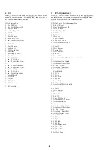
Page 66: ... 2 ARP 1930 8 3 Test Tone Error Codes List 00 Error not detected 01 RAM write read data discord 02 Gate array NG 03 EEPROM NG 08 ARP register read data discord 09 ARP RAM data bus error 10 ARP RAM address bus error 11 ARP RAM read data discord 12 Servo DSP NG 13 1930 SDRAM NG 14 ARP 1930 video NG 15 ARP 1930 audio NG 16 1910 UCODE download NG 17 System call error function not supported 18 System c...

Page 67: ...ough the message to con firm whether discs other than SACD disc are adjusted is not dis played you can finish the adjustment if pressing the STOP but ton During adjustment of each disc the measurement for disc type judgment is made As automatic adjustment does not judge the disc type unlike conventional models take care not to insert wrong type discs Also do not give a shock during adjustment 1 DV...

Page 68: ...llowing steps then adjusted values will be written to the EEPROM DVD Dual Layer Disc Adjustment Steps 1 Sled Tilt Reset 2 Disc Check Memory DL 3 Wait 500 msec 4 Set Disc Type DL 5 LD ON 6 Spdl Start 7 Wait 1 sec Layer 1 Adjust 8 Focus Servo ON 0 9 Auto Track Offset Adjust 10 Clva ON 11 Wait 500 msec 12 Tracking ON 13 Wait 500 msec 14 Sled ON 15 Check CLV Lock 16 Auto Loop Filter Offset Auto Focus ...

Page 69: ...rol and adjustment can be executed manually Drive Manual Operation Operation Menu 1 Disc type 2 Servo Control 3 Track Layer Jump 4 Manual Adjustment 5 Auto Adjustment 6 Memory Check 0 Disc Check Memory Exit Return In using the manual operation menu take care of the following points These commands do not provide protection thus requiring correct operation The sector address or time code field is di...

Page 70: ...isplay field will appear as shown below These values are displayed when PLL is locked Disc Type 1 Disc Type Auto Check 2 DVD SL 12 cm 3 DVD DL 12 cm 4 CD 12cm 5 SACD 12 cm 6 DVD SL 8 cm 7 DVD DL 8 cm 8 CD 8 cm 9 SACD 8 cm 0 Reset SLED TILT SA SI EMG 00 DVD SL 12 cm Display when DVD SL 12cm disc was selected Disc Type 1 Disc Type Auto Check 2 DVD SL 12 cm 3 DVD DL 12 cm 4 CD 12cm 5 SACD 12 cm 6 DVD...

Page 71: ... range of 10 to 80 If extreme value such as 00 or FF is set adjustment will be faulty In such a case check for disc scratch or cable dis connection then perform adjustment again 6 6 MECHA AGING Mecha Aging Press OPEN key Abort STOP key On the Test Mode Menu screen selecting 3 executes the aging of mechanism First open the tray and load a disc Press the PLAY key and the aging will start When the tr...

Page 72: ...n made a request to seek nonexistent address 61 With a CD disc Syscon made a request to seek nonexistent address 62 With a CD disc Syscon made a request to seek nonexistent track No and index No 63 With a DVD disc seeking of target address failed 64 With a CD disc seeking of target address failed 65 With a CD disc seeking of target index failed 70 With a DVD disc physical information data could no...

Page 73: ...A 6 DVD reference disc HLX 501 J 6090 071 A dual layer HLX 503 J 6090 069 A single layer HLX 504 J 6090 088 A single layer HLX 505 J 6090 089 A dual layer 7 SACD reference disc HLXA 509 J 6090 090 A 7 1 POWER SUPPLY ADJUSTMENT 1 Power Supply Check HS 030SF BOARD Mode E E Instrument Digital voltmeter 5 V Check Test point CN202 pin 5 Specification 5 0 0 2 Vdc 3 3 V Check Test point CN202 pin 7 Speci...

Page 74: ... 0 1 Vp p Checking method 1 In the test mode initial menu 6 Video Level Adjustment set so that color bars are generated 2 Confirm that the S Y level is 1 0 0 1 Vp p Figure 7 2 3 Checking Component Video Output B Y MB 85 BOARD Purpose This checks component video output B Y If it is incorrect cor rect colors will not be displayed when connected to for instance projector Mode Video level adjustment i...

Page 75: ... is 1 0 0 1 Vp p Figure 7 5 6 Checking S Video Output S C MB 85 BOARD Purpose This checks whether the S C satisfies the NTSC Standard If it is not correct the colors will be too dark or light Mode Video level adjustment in test mode Signal Color bars Test point CN005 pin 5 Instrument Oscilloscope Specification 286 50 mVp p Connection Checking method 1 Confirm that the S C burst is 286 50 mVp p Fig...

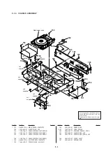
Page 76: ...e electrical parts list SECTION 8 REPAIR PARTS LIST 8 1 EXPLODED VIEWS DVP S533D The components identified by mark or dotted line with mark are criti cal for safety Replace only with part number speci fied Ref No Part No Description Remark Ref No Part No Description Remark 8 1 1 CASE ASSEMBLY 7 4 4 4 6 1 2 3 8 3 5 Front panel section 1 3 975 726 71 EMBLEM DVD 2 3 053 498 31 COVER BK TRAY 3 3 970 6...

Page 77: ...OR POWER 112 X 3949 779 1 RING ASSY SHUTTLE 113 3 054 218 01 BUTTON JOG 114 3 054 224 31 STICK CURSOR 115 1 418 097 11 ENCODER ROTARY 116 4 951 620 01 SCREW 2 6X8 BVTP 117 1 790 167 11 CABLE FLEXIBLE FLAT FMF 35 118 A 6065 316 A FL 101 BOARD COMPLETE 119 3 054 217 31 KNOB VOLUME 120 2 118 268 01 NUT M9 HEXAGON 121 3 684 436 01 PLATE MOUNT 122 A 6065 315 A HP 111 BOARD COMPLETE 123 A 6065 317 A SW ...

Page 78: ...160 3 053 508 61 PANEL REAR 161 1 769 744 91 CORD POWER 162 4 966 267 11 BUSHING FBS001 CORD 163 3 970 608 51 SUMITITE B3 BV 165 3 055 791 01 SUMITITE B3 RING BV 166 3 055 418 01 COVER EJECT 167 3 054 650 01 SPRING EMC 8 1 3 CHASSIS ASSEMBLY 163 162 161 163 152 158 156 155 154 165 165 165 166 152 152 159 151 153 160 163 163 163 163 not supplied not supplied not supplied not supplied not supplied n...

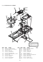
Page 79: ...OADING 213 A 6066 013 A MS 46 BOARD COMPLETE 214 3 053 845 11 CHUCK PLATE 215 3 053 844 11 YOKE 216 3 053 846 11 CHUCK HOLDER 217 3 053 848 11 YOKE HOLDER 218 3 053 847 01 INSULATOR 219 4 981 923 01 SCREW M STEP 220 8 820 081 03 OPTICAL PICK UP KHM 220AAA J1RP 221 3 053 843 11 MOTOR PULLEY 222 3 055 097 01 SEAL DUST TRAY 223 7 621 775 10 SCREW B 2 6X4 M001 1 541 632 11 MOTOR DC LOADING The compone...

Page 80: ...P 220PF 5 50V C344 1 126 960 11 ELECT 1uF 20 50V C345 1 163 021 91 CERAMIC CHIP 0 01uF 10 50V C350 1 163 233 11 CERAMIC CHIP 18PF 5 50V C351 1 163 233 11 CERAMIC CHIP 18PF 5 50V C353 1 163 233 11 CERAMIC CHIP 18PF 5 50V C354 1 163 233 11 CERAMIC CHIP 18PF 5 50V C355 1 163 233 11 CERAMIC CHIP 18PF 5 50V C361 1 164 346 11 CERAMIC CHIP 1uF 16V C362 1 164 346 11 CERAMIC CHIP 1uF 16V C363 1 164 346 11 ...

Page 81: ...ITE 0UH FB319 1 414 553 11 FERRITE 0UH FB320 1 414 553 11 FERRITE 0UH FB321 1 414 553 11 FERRITE 0UH FB322 1 414 553 11 FERRITE 0UH FB341 1 414 135 11 FERRITE 0UH FB342 1 414 553 11 FERRITE 0UH FB401 1 414 553 11 FERRITE 0UH FB402 1 414 553 11 FERRITE 0UH FB403 1 414 553 11 FERRITE 0UH FB404 1 414 553 11 FERRITE 0UH FB405 1 414 553 11 FERRITE 0UH FB406 1 414 553 11 FERRITE 0UH FB407 1 414 553 11 F...

Page 82: ...316 1 216 097 91 RES CHIP 100K 5 1 10W R317 1 216 073 00 METAL CHIP 10K 5 1 10W R318 1 216 097 91 RES CHIP 100K 5 1 10W R319 1 216 097 91 RES CHIP 100K 5 1 10W R320 1 216 097 91 RES CHIP 100K 5 1 10W R321 1 216 073 00 METAL CHIP 10K 5 1 10W R322 1 216 073 00 METAL CHIP 10K 5 1 10W R323 1 216 021 00 METAL CHIP 68 5 1 10W R324 1 216 021 00 METAL CHIP 68 5 1 10W R325 1 216 021 00 METAL CHIP 68 5 1 10...

Page 83: ...70 5 1 10W R461 1 216 041 00 METAL CHIP 470 5 1 10W R501 1 216 089 91 RES CHIP 47K 5 1 10W R502 1 216 069 91 METAL CHIP 6 8K 5 1 10W R503 1 216 089 91 RES CHIP 47K 5 1 10W R504 1 216 069 00 METAL CHIP 6 8K 5 1 10W R510 1 216 069 00 METAL CHIP 6 8K 5 1 10W R511 1 216 069 00 METAL CHIP 6 8K 5 1 10W R512 1 216 071 00 METAL CHIP 8 2K 5 1 10W R513 1 216 069 00 METAL CHIP 6 8K 5 1 10W R514 1 216 071 00 ...

Page 84: ... 10W R226 1 216 025 91 RES CHIP 100 5 1 10W R227 1 216 025 91 RES CHIP 100 5 1 10W R229 1 216 063 91 RES CHIP 3 9K 5 1 10W R230 1 216 073 00 METAL CHIP 10K 5 1 10W R231 1 216 025 91 RES CHIP 100 5 1 10W R232 1 216 025 91 RES CHIP 100 5 1 10W R241 1 216 073 00 METAL CHIP 10K 5 1 10W R243 1 216 073 00 METAL CHIP 10K 5 1 10W R244 1 216 073 00 METAL CHIP 10K 5 1 10W R247 1 216 073 00 METAL CHIP 10K 5 ...

Page 85: ...METAL CHIP 330 5 1 10W SWITCH S071 1 771 349 21 SWITCH KEYBOARD 1 u TRANSFORMER T001 1 433 748 11 TRANSFORMER DC DC CONVERTER A 6065 315 A HP 111 BOARD COMPLETE Ref No 3 000 Series CONNECTOR CN701 1 564 013 11 PIN CONNECTOR 3P DIODE D701 8 719 071 15 DIODE HZM6 8ZWA1TL D702 8 719 071 15 DIODE HZM6 8ZWA1TL FERRITE BEAD FB701 1 414 135 11 FERRITE 0UH FB702 1 414 135 11 FERRITE 0UH FB703 1 414 135 11...

Page 86: ...25V C439 1 125 822 11 TANTALUM 10uF 20 10V C440 1 125 822 11 TANTALUM 10uF 20 10V C441 1 126 209 11 ELECT CHIP 100uF 20 4V C443 1 162 970 11 CERAMIC CHIP 0 01uF 10 25V C505 1 162 970 11 CERAMIC CHIP 0 01uF 10 25V C506 1 162 970 11 CERAMIC CHIP 0 01uF 10 25V C508 1 162 970 11 CERAMIC CHIP 0 01uF 10 25V C510 1 162 970 11 CERAMIC CHIP 0 01uF 10 25V C512 1 162 970 11 CERAMIC CHIP 0 01uF 10 25V C601 1 ...

Page 87: ... 21 FERRITE 0UH FB002 1 469 324 21 FERRITE 0UH FB003 1 469 324 21 FERRITE 0UH FB004 1 469 324 21 FERRITE 0UH FB005 1 469 324 21 FERRITE 0UH FB006 1 469 324 21 FERRITE 0UH FB007 1 469 324 21 FERRITE 0UH FB008 1 469 324 21 FERRITE 0UH FB010 1 469 116 21 FERRITE 0UH FB011 1 469 116 21 FERRITE 0UH FB012 1 469 116 21 FERRITE 0UH FB014 1 469 116 21 FERRITE 0UH FB015 1 469 116 21 FERRITE 0UH FB016 1 216 ...

Page 88: ... TRANSISTOR 2SC4116 YG Q803 8 729 230 63 TRANSISTOR 2SC4116 YG RESISTOR R001 1 216 833 11 METAL CHIP 10K 5 1 16W R002 1 216 833 11 METAL CHIP 10K 5 1 16W R003 1 216 833 11 METAL CHIP 10K 5 1 16W R004 1 216 821 11 METAL CHIP 1K 5 1 16W R005 1 216 821 11 METAL CHIP 1K 5 1 16W R006 1 216 821 11 METAL CHIP 1K 5 1 16W R007 1 216 864 11 METAL CHIP 0 5 1 16W R009 1 216 864 11 METAL CHIP 0 5 1 16W R010 1 ...

Page 89: ... 1 216 809 11 METAL CHIP 100 5 1 16W R643 1 216 815 11 METAL CHIP 330 5 1 16W R647 1 216 833 11 METAL CHIP 10K 5 1 16W R701 1 216 805 11 METAL CHIP 47 5 1 16W R702 1 216 817 11 METAL CHIP 470 5 1 16W R703 1 216 817 11 METAL CHIP 470 5 1 16W R704 1 216 817 11 METAL CHIP 470 5 1 16W R705 1 216 817 11 METAL CHIP 470 5 1 16W R706 1 216 821 11 METAL CHIP 1K 5 1 16W R707 1 216 844 11 METAL CHIP 82K 5 1 ...

Page 90: ...RATOR X001 1 781 188 21 OSCILLATOR CRYSTAL 27MHz X201 1 781 185 21 VIBRATOR CERAMIC 12 5MHz A 6066 013 A MS 46 BOARD COMPLETE Ref No 3 000 Series CONNECTOR CN001 1 564 722 11 PIN CONNECTOR SMALL TYPE 6P SWITCH S001 1 771 562 11 SWITCH LEVER TRAY SENSOR S002 1 762 386 11 SWITCH PUSH CHUCK SENSOR 1 468 359 21 POWER BLOCK HS 030SF Ref No 6 000 Series CAPACITOR C110 9 884 093 01 ELECT 220uF 400V C131 ...

Page 91: ... 172 11 CERAMIC CHIP 0 0056uF 10 25V C020 1 107 826 91 CERAMIC CHIP 0 1uF 10 16V C021 1 107 826 91 CERAMIC CHIP 0 1uF 10 16V C022 1 107 826 91 CERAMIC CHIP 0 1uF 10 16V C023 1 165 176 11 CERAMIC CHIP 0 047uF 10 16V C024 1 164 730 11 CERAMIC CHIP 0 0012uF 10 50V C025 1 165 176 11 CERAMIC CHIP 0 047uF 10 16V C026 1 162 964 11 CERAMIC CHIP 0 001uF 10 50V C027 1 164 217 11 CERAMIC CHIP 150PF 5 50V C02...

Page 92: ...167 11 CABLE FLEXIBLE FLAT FMF 35 153 1 790 166 11 CABLE FLEXIBLE FLAT FMT 25 154 1 790 163 11 CABLE FLEXIBLE FLAT FMA 7 155 1 790 164 11 CABLE FLEXIBLE FLAT FMA 8 156 1 790 165 11 CABLE FLEXIBLE FLAT FMA 9 161 1 769 744 91 CORD POWER 220 8 820 081 03 OPTICAL PICK UP KHM 220AAA J1RP M001 1 541 632 11 MOTOR DC LOADING ACCESSORIES PACKING MATERIALS 1 418 320 21 COMMANDER STANDARD RMT D108A 1 569 008...

Page 93: ... 138 DVP S533D Sony Corporation Home Video Company 9 921 727 11 99G05009 1D Printed in Japan 1999 7 Published by Quality Assurance Dept ...

Reviews: