background image

CHASSIS

SERVICE MANUAL

SPECIFICATIONS

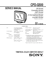
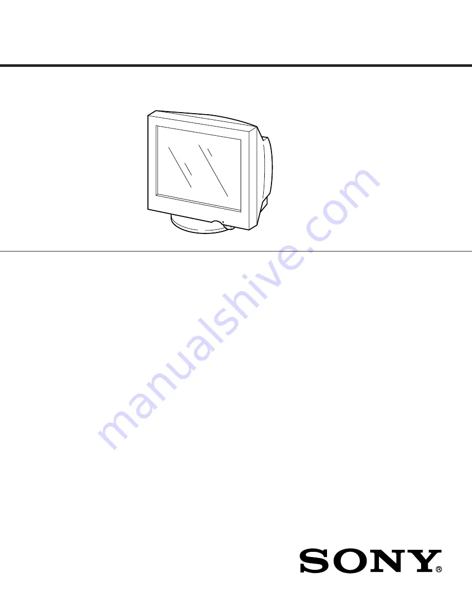
CPD-G500

G1

US Model

Canadian Model

AEP Model

Chassis No. SCC-L22C-A

S.Hemisphere Model

Chassis No. SCC-L22G-A

Equator Model

Chassis No. SCC-L22F-A

TRINITRON

®

 COLOR COMPUTER DISPLAY

CRT

0.24 mm aperture grille pitch 
21 inches measured diagonally 
90-degree deflection
FD Trinitron

Viewable image size

Approx. 403.8 

×

 302.2 mm (w/h) 

(16  

×

 12 inches) 

19.8" viewing image

Resolution

Maximum

Horizontal: 2048 dots
Vertical: 1536 lines

Recommended

Horizontal: 1600 dots
Vertical: 1200 lines

Standard image area

Approx. 388 

×

 291 mm (w/h) 

(15 

3

/

8


×

 11 

1

/

2

 inches) 

or 
Approx. 364 

×

 291 mm (w/h) 

(14 

3

/

8


×

 11 

1

/

2

 inches)

Deflection frequency*

Horizontal: 30 to 121 kHz
Vertical: 48 to 160 Hz

AC input voltage/current  100 to 240 V, 50 – 60 Hz, 2.0 – 1.0 A
Power consumption

Approx. 145 W

Dimensions

Approx. 497 

×

 480 

×

 478 mm (w/h/d) 

(19 

5

/

8


×

 19 

×

 18 

7

/

8

 inches)

Mass

Approx. 32 kg (70 lb 9 oz)

Plug and Play

DDC1/2B/2Bi, GTF**

* Recommended horizontal and vertical timing condition

• Horizontal sync width duty should be more than 4.8% of total 

horizontal time or 0.8 

µ

s, whichever is larger.

• Horizontal blanking width should be more than 2.3 

µ

sec.

• Vertical blanking width should be more than 450 

µ

sec.

** If the input signal is Generalized Timing Formula (GTF) 

compliant, the GTF feature of the monitor will automatically 
provide an optimal image for the screen.

Design and specifications are subject to change without notice.

Summary of Contents for FD Trinitron CPD-G500

Page 1: ...m w h 14 3 8 11 1 2 inches Deflection frequency Horizontal 30 to 121 kHz Vertical 48 to 160 Hz AC input voltage current 100 to 240 V 50 60 Hz 2 0 1 0 A Power consumption Approx 145 W Dimensions Approx 497 480 478 mm w h d 19 5 8 19 18 7 8 inches Mass Approx 32 kg 70 lb 9 oz Plug and Play DDC1 2B 2Bi GTF Recommended horizontal and vertical timing condition Horizontal sync width duty should be more ...

Page 2: ...OMPOSANTS IDENTIFIÉS PAR UNE TRAME ET UNE MARQUE SONT CRITIQUES POUR LA SÉCURITÉ NE LES REMPLACER QUE PAR UNE PIÈCE PORTANT LE NUMÉRO SPECIFIÉ LES RÉGLAGES DE CIRCUIT DONT L IMPORTANCE EST CRITIQUE POUR LA SÉCURITÉ DU FONCTIONNEMENT SONT IDENTIFIÉS DANS LE PRÉSENT MANUEL SUIVRE CES PROCÉDURES LORS DE CHAQUE REMPLACEMENT DE COMPOSANTS CRI TIQUES OU LORSQU UN MAUVAIS FONCTIONNEMENT EST SUSPECTÉ Afte...

Page 3: ...p green the monitor is working properly If the 1 power indicator is still flashing there is a potential monitor failure Count the number of seconds between orange flashes of the 1 power indicator and inform your authorized Sony dealer of the monitor s condition Be sure to note the model name and serial number of your monitor Also note the make and model of your computer and video board MENU RESET ...

Page 4: ... H BLK 2 440 2 424 2 271 2 267 H FP 0 279 0 485 0 668 0 480 H SYNC 0 837 0 754 0 481 0 667 H BP 1 325 1 185 1 122 1 120 H ACTIV 6 972 6 465 6 011 6 000 VERTICAL V FREQ HZ 85 000 Hz 75 000 Hz 80 120 Hz 85 009 Hz lines lines lines lines V TOTAL 1250 1500 1507 1423 V BLK 50 60 67 73 V FP 1 1 1 1 V SYNC 3 3 3 3 V BP 46 56 63 69 V ACTIV 1200 1440 1440 1350 SYNC INT G NO NO NO NO EXT H V POLARITY YES P ...

Page 5: ...mbly Removal 2 2 2 5 N Board Removal 2 3 2 6 Service Position 2 3 2 7 Bezel Assembly H1 Board Removal 2 4 2 8 Picture Tube Removal 2 4 2 9 J Board Removal 2 5 2 10 Harness Location 2 6 3 SAFETY RELATED ADJUSTMENT 3 1 4 ADJUSTMENTS 4 1 5 DIAGRAMS 5 1 Block Diagrams 5 1 5 2 Frame Shcematic Diagram 5 7 5 3 Circuit Boards Location 5 9 5 4 Schematic Diagrams and Printed Wiring Boards 5 9 1 Schematic Di...

Page 6: ... Do not use any type of abrasive pad scouring powder or solvent such as alcohol or benzene Transportation When you transport this monitor for repair or shipment use the original carton and packing materials Use of the tilt swivel This monitor can be adjusted within the angles shown below To find the center of the monitor s turning radius align the center of the monitor s screen with the centering ...

Page 7: ...the monitor then connect it to a power outlet Step 3 Turn on the monitor and computer First turn on the monitor then turn on the computer The installation of your monitor is complete If necessary use the monitor s controls to adjust the picture If no picture appears on your screen Check that the monitor is correctly connected to the computer If NO INPUT SIGNAL appears on the screen try changing th...

Page 8: ...ontrol button to display the main MENU on your screen See page 10 for more information on using the control button Use the control button to select one of the following menus x Displaying the current input signal The horizontal and vertical frequencies of the current input signal are displayed in the main MENU If the signal matches one of this monitor s factory preset modes the resolution is also ...

Page 9: ... First move the control button m M to select AUTO Then move the control button The picture automatically fills the screen Notes This function is intended for use with a computer running Windows or similar graphic user interface software that provides a full screen picture It may not work properly if the background color is dark or if the input picture does not fill the screen to the edges such as ...

Page 10: ...trol button m M to select the desired adjustment item Then move the control button to make the adjustment Moire is a type of natural interference which produces soft wavy lines on your screen It may appear due to interference between the pattern of the picture on the screen and the phosphor pitch pattern of the monitor Note The picture may become fuzzy when CANCEL MOIRE is set to ON Adjusting the ...

Page 11: ...e original factory quality levels The explanation below explains how to restore the monitor s color from the EASY menu 1 Move the control button to select EASY or sRGB mode 2 First move the control button m M to select IMAGE RESTORATION Then move the control button The picture disappears while the color is being restored about 2 seconds After the color is restored the picture reappears on the scre...

Page 12: ...e the input signal is cut and NO INPUT SIGNAL appears on the screen After a few seconds the monitor enters a power saving mode RESET Power mode Power consumption 1 power indicator normal operation 145 W green 1 standby 100 W green and orange alternate 2 suspend sleep 15 W green and orange alternate 3 active off deep sleep Approx 1 W orange power off 0 W off 17 US Troubleshooting Before contacting ...

Page 13: ...en if the frequency is within the proper range some video boards may have a sync pulse that is too narrow for the monitor to sync correctly Adjust the computer s refresh rate vertical frequency to obtain the best possible picture Picture is fuzzy Adjust the brightness and contrast page 10 Degauss the monitor page 15 If CANCEL MOIRE is ON the picture may become fuzzy Decrease the moire cancellation...

Page 14: ...ndicator and inform your authorized Sony dealer of the monitor s condition Be sure to note the model name and serial number of your monitor Also note the make and model of your computer and video board Specifications CRT 0 24 mm aperture grille pitch 21 inches measured diagonally 90 degree deflection FD Trinitron Viewable image size Approx 403 8 302 2 mm w h 16 12 inches 19 8 viewing image Resolut...

Page 15: ...ews BVTT 4 x 8 4 Two screws BVTP 4 x 16 Push in the tip of a screwdriver about 5mm to unlock the claw A B Three screws BVTT 4 x 8 Two screws BVTP 3 x 12 D board Screw P 3 5 x 20 Open the D block in the direction of the arrow and remove of the arrow Two hooks 5 A B CN504 CN505 GND 1 2 3 4 2 1 CABINET REMOVAL SECTION 2 DISASSEMBLY 2 2 D BOARD REMOVAL 2 1 ...

Page 16: ...Two printed circuit board holders 2 1 Two screws BVTP 3 x 8 7 AC inlet 3P 8 5 3 4 6 A board 2 2 Four screws BVTT 4 x 8 1 Two screws HD15 4 I O terminal board assembly 5 3 A board 1 2 A board 1 2 A board 1 2 Screw lock 2 When installing I O terminal board assembly be sure to apply screw lock on 2 spots after screws HD15 are fixed 2 3 G BOARD REMOVAL 2 4 A BOARD I O TERMINAL BOARD ASSEMBLY REMOVAL 2...

Page 17: ...to 2 2 CN602 Rear shield D G boards G board Refer to 2 3 AC inlet 3P CAUTION SHORT If the claw is hooked opening and closing the board is impossible Do not try to do it by force If the claw is hooked opening and closing the board is impossible Do not try to do it by force 2 5 N BOARD REMOVAL 2 6 SERVICE POSITION 2 3 ...

Page 18: ...g screw 5 H1 board Two screws BVTP 4 x 16 Bezel assembly 2 Before removing the bezel assembly secure the picture tube by attaching two screws to the picture tube shield at the positions shown with an arrow diagonal two places to prevent the picture tube from falling Use the screws BVTT 4 x 8 that fix top cover 1 3 Input selection CN801 Picture tube shield Two H printed circuit board brackets Menu ...

Page 19: ...f anode caps with shartp shaped material 2 Don t press the rubber hardly not to damage inside of anode caps A material fitting called as shatter hook terminal is built in the rubber 3 Don t turn the foot of rubber over hardly The shatter hook terminal will stick out or damage the rubber REMOVAL OF ANODE CAP NOTE Short circuit the anode of the picture tube and the anode cap to the metal chassis CRT...

Page 20: ...N509 CN506 CN502 CN505 CN501 CN508 CN4 CN007 CN011 CN010 CN402 CN405 CN407 CN408 CN403 CN406 CN504 FBT CN651 G board N board AC inlet A board I O terminal board assembly D board Rear shield Picture tube J board H1 board CN650 CN652 CN653 CN654 4pin 4pin 2 6 2 10 HARNESS LOCATION ...

Page 21: ...e D board and check that high voltage checked in 1 lowers by 1 50 kV or more when the specified cur rent flows to the pin Specification 2 00 0 00 0 01 mA d Beam Current Protector Circuit Check 2nd Protector D Board 1 Connect constant current source to a section between T902 FBT pin and pin GND on the D board and check that the voltage of CN504 0 pin becomes 0 V or less when the specified current f...

Page 22: ... Adjust so that the green is within the specification given right 4 corner adjust target within 1 The red and blue must be within the specification given right with respect to the green A difference between red and blue must be within the specification given right 0 3 0 7 5 0 3 0 3 0 7 5 0 3 0 3 0 7 5 0 3 µm µm 10 10 10 10 7 10 10 10 10 µm Adjustment and measurement should be made at the points on...

Page 23: ...her 3 Make rough adjustment of the H and V direction conver gence by using 4 fold poles magnet White Balance Adjustment Specification 1 9300K x 0 283 0 005 y 0 298 0 005 All White 2 6500K x 0 313 0 005 y 0 329 0 005 All White 3 5000K x 0 346 0 005 y 0 359 0 005 All White Vertical and Horizontal Position and Size Specification Focus adjustment Adjust the focus volume 1 and 2 for the optimum focus C...

Page 24: ...CPD G500 4 3 MEMO ...

Page 25: ... 26 25 24 4 3 5 6 7 5 3 1 2 4 4 5 8 1 2 5 2 5 2 1 3 3 9 1 5 14 3 6 7 8 14 13 15 14 13 ROUT GOUT BOUT GND RCI GCI BCI PWM1 XT1 XT0 H SYNC V SYNC HFBP SCL SDA SCL SDA VS Hfly RIN GIN BIN IC406 CUTOFF AMP X401 8MHz G2 CONT Q406 407 410 IC405 1 2 PWM2 PWM3 PWM4 BUFFER Q101 Q201 Q301 9 1 2 4 6 8 HEATER STBY 5V 1W 5V 80V 220V 12V 5V 5V 2 80V 220V 12V PS401 1A CN405 G2 1 G2 CN406 5 3 1 7 KR KG KB HEATER ...

Page 26: ...RXD 15V 15V 15V 15V STBY 5V S0 S6 2 3 4 5 7 1 12 14 16 23 10 18 20 25 22 6 8 S4 S3 S5 S2 S1 TH DET PWR SW DGUS SW HTR SW VRET ECO SW HFBP HD VSHAPE 12V STBY 5V 1W 5V CN002 IC001 CPU DSP CN001 CN010 Q009 IC006 AIN0 Q010 Q012 N µ COM V CONV H CONV LCC GEO MAGNETIC SENSOR A B C D CN011 ECO SW HFBP HD VSP 12V STBY 5V 1W 5V 15V 15V STBY 5V SOG DET D SCL D SDA HSOUT VS OSD HFBP HS1 VC1 HS2 VC2 VS1 SDA1 ...

Page 27: ...CENT H H CENT N H CENT L 220V 220V CN654 6 4 1 2 80V 15V 12V 15V CN653 4 6 8 9 1 2 80V 220V 12V HEATER SYBY 5V 1W 5V CN652 2 1 3 6 4 5 1W 5V STBY 5V ECO SW HTR SW PWR SW DGUS SW CN650 PROTECTOR POWER SW Q650 654 667 Q603 REG OUT START UP VCC SW Q631 633 HEATER SW Q671 RELAY DRV Q691 IC630 REG REG SW Q630 IC653 1W 5V REG IC652 STBY 5V REG IC651 HEATER REG VCC OUT CTL VCC OUT CTL VADJ 1 2 2 4 1 4 1 ...

Page 28: ... LED0 LED1 B IN 2 G GND 2 G IN 2 R GND 2 R IN 2 GND GND B GND 2 ROTATION 15V GND GND GND N C 220V 220V HTR SW 80V 15V 12V GND STBY 5V 1W 5V ECO SW PWR SW DGUS SW STBY 5V RXD TXD GND GND H DY H H DY H H DY C H DY C NC NC V DY H V DY C GND NC GND CHASSIS GND N C G2 1W 5V GND STBY 5V N C AC L AC N PWR SW DGUS SW HTR SW DGC N C N C DGC H CENT H 220V 220V N C GND GND H CENT N H CENT L GND 15V GND GND 1...

Page 29: ...ns may be noted due to normal production tolerances Can not be measured Circled numbers are waveform references s B bus S B bus Note The components identified by shading and mark are critical for safety Replace only with part number specified Note Les composants identifiés par un tramé et une marque sont critiques pour la sécurité Ne les remplacer que par une pièce portant le numéro spécifié Part ...

Page 30: ...70k CHIP 470k CHIP 470k CHIP 470k CHIP 470k CHIP 22k CHIP 10k CHIP 1k CHIP 0 1 25V B CHIP 0 1 25V B CHIP 0 1 25V B CHIP 1 250V HSS83TD HSS83TD HSS83TD 470 470 470 100k CHIP 220k CHIP 0 01 B CHIP 0 01 B CHIP 0 01 B CHIP 0 01 B CHIP 0 01 B CHIP 0 01 B CHIP 100p CH CHIP 0 22 0 01 B CHIP 21P L FPC 1SS119 2 2M CHIP 100 CHIP 100 CHIP 47 CHIP 47 CHIP 100 CHIP 10k CHIP 100k CHIP 470k CHIP 470k CHIP 470k C...

Page 31: ...RETRACE BLANKING 41 30 34 42 6 9 5 3 CLAMP SUB CONTRAST MAIN CONTRAST OSD MIX AMP CLAMP F B RETRACE BLANKING 38 11 13 10 8 17 16 21 25 26 27 28 29 32 36 39 14 1 12 20 7 CLAMP SUB CONTRAST MAIN CONTRAST OSD MIX DAC BUS I F AMP CLAMP F B OSD LEVEL 4bit Main CONTRAST 8bit B SUB CONT 8bit G SUB CONT 8bit R SUB CONT 8bit RETRACE BLANKING 33 35 31 24 22 23 19 Sync On Green Sep OSD BLK IN INPUT R VCC1 R ...

Page 32: ...9 D403 A 2 A 2 D405 D 3 D 1 D406 D 2 6 D407 D 2 6 CRYSTAL X401 C 2 C 2 5 15 5 16 Schematic diagram Ò A A A A A board A BOARD Component Side A BOARD Conductor Side A VIDEO AMP RGB OUT A BOARD SEMICONDUCTOR LOCATION Component Side Refer to Terminal name of semiconductors in silk screen printed circuit see page 5 10 Conductor Side NOTE The circuit indicated as left contains high voltage of over 600 V...

Page 33: ...Q803 Q804 Q801 Q802 100k 47 16V SPR 325MVW 1k 10k 10k 10K 11P WHT L S MICRO 22k 47 16V 10k RN 150 470 1k 1 5k RN RN RN RN 2SA1309A LED DRIVE 2SA1309A LED DRIVE 2SC3311A LED DRIVE 2SC3311A LED DRIVE LED0 LED1 KEY_DET STBY 5V GND GND GND GND 1W 5V BNC HD15 RESET INPUT MENU POWER INPUT_SW ENV_DRI H1 USER CONTROL TO N a BOARD CN007 CRT SHIELD TO B SS3484 J H1 EPS05 R802 R803 R804 470 220 220 R851 470 ...

Page 34: ...2p 500V CH 1 1 2W FUSE 47k 47k 47k 1 1 2W FPRD 6800p B CHIP 1k CHIP 4 7 FPRD 4 7 FPRD 470 FPRD 1k CHIP 10k CHIP 47k CHIP 330k 1 2W RC 4 7k 1 2W RC 1k 1 2W RC 4 7 FPRD 1k CHIP 1 2k RN CP 1 2k RN CP 1k 1 2W RC 0 22 MPS 6 8 3W RS 0 01 B CHIP 0 01 B CHIP 1mH 100 25V 470 16V 100 25V 4700p 100V PT 4700p 2kV E 1k CHIP 10 R921 10k 47 0 1 B CHIP 10k RN CP 100k 470 16V 25V 4 7k CHIP 100 25V 680k RN CP 47k C...

Page 35: ...ust be paid to prevent an electric shock in inspection or repairing 1 2 3 4 6 5 D BOARD WAVEFORMS 54 5 Vp p H 1 9 Vp p H 2 1 Vp p H 568 Vp p H 8 8 Vp p H 50 6 Vp p H D BOARD SEMICONDUCTOR LOCATION Refer to Terminal name of semiconductors in silk screen printed circuit see page 5 10 DIODE D504 D 4 3 D505 A 1 D506 A 4 D507 A 2 D508 A 3 D509 B 2 D510 A 1 D511 A 2 D512 B 3 3 D513 B 2 D514 B 3 D515 B 2...

Page 36: ...HIP 100 CHIP 100 CHIP 100 CHIP 100 CHIP 100 CHIP 100 CHIP 1k CHIP 1k CHIP 10k CHIP 2 2k CHIP 0 001 B CHIP 1k CHIP 1k CHIP 10k CHIP R046 10k CHIP 0 01 B CHIP 10 0 01 B CHIP 10 MA151WK TX MA151WK TX MA151WK TX 1PS226 115 1k CHIP 1k CHIP 100 CHIP 100 CHIP 1SS355TE 17 100µH 1k CHIP HZS5 6NB2TD HZS5 6NB2TD HZS5 6NB2TD HZS5 6NB2TD 5 6k CHIP 100 CHIP 0 22 MPS 1000 25V 0 1 25V B CHIP 0 1 25V B CHIP 21P FF...

Page 37: ... 0 022 B CHIP 0 022 B CHIP 0 022 B CHIP 0 01 B CHIP 1k CHIP1k CHIP 1k CHIP1k CHIP 10k CHIP 10k CHIP 4 7k CHIP 1k CHIP1k CHIP 1k CHIP 1k CHIP 1k CHIP 10k CHIP 4 7k CHIP 4 7k CHIP 4 7k CHIP 0 1 B CHIP 2200p CH CHIP 1k CHIP 2 2k CHIP 2 2k CHIP 1k CHIP 1k CHIP 1k CHIP 1k CHIP 1k CHIP 1k CHIP 1k CHIP 0 01 B CHIP 0 1 B CHIP 100 CHIP 1k CHIP 0 01 B CHIP 1k CHIP 1SS355TE 17 1SS355TE 17 2 2k CHIP 10k CHIP ...

Page 38: ... 25V 22 1W RS 22 1W RS 6 8k CHIP 100k CHIP 4 7 CHIP 100k CHIP 120 2W RS 150 2W RS 10k CHIP 10k CHIP 10k CHIP 10k CHIP 10k CHIP 22k CHIP 22k CHIP 47 0 1 B CHIP 0 1 25V B CHIP 0 01 B CHIP 1 1µH 1 1µH 1 1µH 1 1µH 1 1µH 1 1µH 1 1µH 0 1 25V B CHIP 1 2 FPRD 1 2 FPRD 1 2 FPRD 1 2 FPRD 0 1 25V B CHIP 0 1 25V B CHIP 0 1 25V B CHIP 0 1 25V B CHIP 0 1 25V 25V B CHIP 0 1 25V B CHIP 0 1 25V B CHIP 0 1 B CHIP 0...

Page 39: ...C 2 C 2 D015 B 2 8 D016 B 1 B 2 D017 B 1 B 2 D018 B 1 B 2 D020 B 1 3 D021 C 3 3 D022 C 3 8 D023 B 2 8 D024 B 2 8 D025 B 1 6 D026 B 2 6 D027 D 2 3 D028 D 2 3 D029 D 3 D 1 D036 D 3 D 1 D037 D 3 D 1 D038 C 1 3 CRYSTAL X001 C 2 C 1 5 29 5 30 N µ COM V CONV H CONV LCC GEO MAGNETIC SENSOR N BOARD Component Side N BOARD Conductor Side N BOARD SEMICONDUCTOR LOCATION Refer to Terminal name of semiconductor...

Page 40: ...2200 10V D4SBS4 470 D4SBL40 0 01 PT ON3171 R 1 275V 0 22 MPS 47 1SS119 1SS119 0 45µH 68µH 100 10 4700p PT 0 1 B CHIP 7P WHT S MICRO 9P WHT S MICRO 6P WHT S MICRO 8P WHT S MICRO 1SS119 47k CHIP 470k CHIP 4 7k CHIP 10k CHIP 1k CHIP 10k CHIP 2 2k CHIP 47k CHIP 10k CHIP 2 2k CHIP 10k CHIP 1k CHIP 220 CHIP 10k CHIP 4 7k CHIP 1SS119 100 100 25V D1NL20U D1NL20U D1NL20U RD22ESB2 RD12ESB2 RD22ESB2 1SS119 R...

Page 41: ...0 C 3 IC650 A 1 IC651 C 1 IC652 C 1 IC653 C 1 IC654 B 1 IC680 C 2 TRANSISTOR Q603 A 3 Q610 C 2 Q621 C 3 Q630 C 3 Q631 B 3 Q632 C 3 Q633 C 3 1 Q650 B 2 Q651 B 1 Q652 C 1 1 Q653 B 1 1 Q654 B 2 1 Q667 C 1 1 Q670 C 2 1 Q671 C 1 1 Q691 C 2 DIODE D610 B 4 D612 C 2 D613 A 4 D620 C 2 D631 C 2 D632 B 3 D633 B 3 D634 C 3 D635 C 3 D637 C 3 D650 A 2 D651 B 2 D652 A 1 D653 A 2 D654 A 1 D655 B 2 D656 B 2 D660 B...

Page 42: ...8pin SOP 20pin SOP 18pin SOP 160pin QFP 28pin SOP 5pin SIP 8pin DIP 15pin SIP 1 3 8 10 17 MARKING SIDE VIEW 1 1 18 19 36 7pin SIP 42pin SOP 36pin SOP 1 2 3 2SC4015TV2 2SC5570 LBSONY 2SD2394 EF 2SJ569LS CB11 2SK2655 01R F165 2SK3262 01MR F119 2SK2103T100 2SK2647 01MR F91 D1NL20U TR D2S4MF D2S4MTA1 D4SB60L D4SBL40 D4SBS4 D4SBS4 F D5SC4M MA151WK TX 1SS184 EGP10D EGP10GPKG23 ERA91 02 ERA91 02TP1 ERA22...

Page 43: ...ER PRINTED CIRCUIT BOARD 6 4 070 730 01 HOLDER PRINTED CIRCUIT BOARD 7 A 1316 443 B G BOARD COMPLETE U C AEP SH EQ for Japan made set 7 A 1316 481 A G BOARD COMPLETE U C for Mexico made set 7 A 1316 480 A G BOARD COMPLETE AEP for UK made set 8 1 251 382 31 INLET AC 3P WITH NOISE FILTER 9 4 070 122 01 SCREW HD15 10 1 694 569 11 TERMINAL BOARD ASSY I O 11 A 1298 874 D A BOARD COMPLETE U C AEP SH EQ ...

Page 44: ...de set 57 4 394 972 21 CAP POWER 58 X 4036 844 2 STAND ASSY 59 59 4 061 996 11 CUSHION 60 8 738 813 61 ITC ASSY 21TKC R1 U C AEP 61 63 60 8 738 821 61 ITC ASSY 21TKC RS1 61 63 SH EQ for Japan made set 61 8 451 509 11 DEFLECTION YOKE Y21TKM M 62 1 452 912 61 NECK ASSEMBLY NA 2914 63 2 162 100 21 SPACER DEFLECTION YOKE 64 4 047 316 01 SPRING EXTENSION Except U C for Mexico made set 64 4 061 573 01 S...

Page 45: ...YETHYLENE U C AEP SH EQ for Japan made set 104 4 368 079 01 BAG POLYETHYLENE AEP for UK made set 104 4 047 293 01 BAG POLYETHYLENE U C for Mexico made set 105 1 793 504 11 CABLE ASSY 15P DSUBX2 CONNECTOR 106 3 867 232 12 MANUAL INSTRUCTION U C SH EQ for Japan made set 106 3 867 232 21 MANUAL INSTRUCTION AEP for Japan made set 106 3 867 232 31 MANUAL INSTRUCTION U C for Mexico made set 106 3 867 23...

Page 46: ...CPD G500 MEMO 6 4 ...
Page 47: ...V C220 1 104 341 11 FILM 0 1µF 10 250V C301 1 163 021 91 CERAMIC CHIP0 01µF 10 50V C302 1 104 664 11 ELECT 47µF 20 25V C303 1 163 021 91 CERAMIC CHIP0 01µF 10 50V C304 1 104 664 11 ELECT 47µF 20 25V C307 1 164 004 11 CERAMIC CHIP0 1µF 10 25V C308 1 164 004 11 CERAMIC CHIP0 1µF 10 25V C309 1 163 227 11 CERAMIC CHIP10pF 0 5pF 50V C310 1 163 275 11 CERAMIC CHIP0 001µF 5 50V C312 1 164 489 11 CERAMIC ...

Page 48: ...IODE 1SS376TE 17 D402 8 719 801 78 DIODE 1SS184 D403 8 719 982 36 ZENER DIODE MTZJ 39B D405 8 719 911 19 DIODE 1SS119 25 D406 8 719 062 51 DIODE 1PS226 115 D407 8 719 062 51 DIODE 1PS226 115 FERRITE BEAD FB102 1 500 419 22 FERRITE FB202 1 500 419 22 FERRITE FB302 1 500 419 22 FERRITE FB402 1 412 911 11 FERRITE 1 1µH FB403 1 412 911 11 FERRITE 1 1µH FB404 1 412 911 11 FERRITE 1 1µH FB405 1 412 911 ...

Page 49: ...RES CHIP 22K 5 1 10W R328 1 216 065 91 RES CHIP 4 7K 5 1 10W R330 1 216 113 00 RES CHIP 470K 5 1 10W R337 1 249 413 11 CARBON 470 5 1 4W R338 1 216 017 91 RES CHIP 47 5 1 10W R361 1 216 041 00 RES CHIP 470 5 1 10W R402 1 216 049 91 RES CHIP 1K 5 1 10W R403 1 216 081 00 RES CHIP 22K 5 1 10W R404 1 216 057 00 RES CHIP 2 2K 5 1 10W R405 1 216 049 91 RES CHIP 1K 5 1 10W R406 1 216 097 91 RES CHIP 100K...

Page 50: ...52 1 128 563 11 ELECT 100µF 20 100V C653 1 128 581 11 ELECT 4 7µF 20 100V C654 1 126 943 11 ELECT 2200µF 20 25V C655 1 104 664 11 ELECT 47µF 20 25V C656 1 126 943 11 ELECT 2200µF 20 25V C657 1 104 664 11 ELECT 47µF 20 25V C658 1 126 927 11 ELECT 2200µF 20 10V C659 1 128 339 11 ELECT 2200µF 20 10V C660 1 126 967 11 ELECT 47µF 20 50V C661 1 107 429 11 CERAMIC 0 0022µF 10 1KV C662 1 137 370 11 FILM 0...

Page 51: ...0 28 TRANSISTOR 2SC1623 L5L6 Q654 8 729 026 49 TRANSISTOR 2SA1037AK T146 R Q667 8 729 026 49 TRANSISTOR 2SA1037AK T146 R Q670 8 729 026 49 TRANSISTOR 2SA1037AK T146 R Q671 8 729 026 49 TRANSISTOR 2SA1037AK T146 R Q691 8 729 119 78 TRANSISTOR 2SC2785 HFE RESISTOR R601 1 220 825 91 CARBON 330K 5 1 2W R602 1 216 465 11 METAL OXIDE 27K 5 2W F R603 1 247 895 91 CARBON 470K 5 1 4W R604 1 216 113 00 RES ...

Page 52: ...ORMER CONVERTER PIT T621 1 429 992 11 TRANSFORMER CONVERTER PRT T630 1 433 895 31 TRANSFORMER CONVERTER SRT THERMISTOR TH601 1 809 260 11THERMISTOR POWER THP601 1 809 827 31THERMISTOR POSITIVE VARISTOR VDR601 1 801 268 51VARISTOR TNR14V471K660 VDR602 1 810 622 11VARISTOR A 1346 827 B D BOARD COMPLETE U C AEP SH EQ for Japan made set A 1346 860 A D BOARD COMPLETE U C for Mexico made set A 1346 859 ...

Page 53: ...0pF 10 2KV C706 1 164 004 11 CERAMIC CHIP0 1µF 10 25V C707 1 130 495 00 FILM 0 1µF 5 50V C708 1 126 942 61 ELECT 1000µF 20 25V C709 1 163 021 91 CERAMIC CHIP0 01µF 10 50V C710 1 107 894 11 ELECT 220µF 20 35V C711 1 163 019 00 CERAMIC CHIP0 0068µF 10 50V C712 1 106 228 00 MYLAR 0 22µF 10 100V C713 1 126 942 61 ELECT 1000µF 20 25V C715 1 164 004 11 CERAMIC CHIP0 1µF 10 25V C720 1 126 964 11 ELECT 10...

Page 54: ...FB901 1 410 397 21 FERRITE 1 1µH IC IC501 8 759 585 82 IC BA9759F E2 IC502 8 759 803 42 IC LA6500 FA IC503 8 759 058 50 IC XRA10324AF IC701 8 759 444 82 IC LA7841L IC901 8 759 585 81 IC BA9758FS E2 CHIP CONDUCTOR JR002 1 216 296 91 SHORT 0 JR003 1 216 295 91 SHORT 0 JR004 1 216 295 91 SHORT 0 JR005 1 216 296 91 SHORT 0 JR006 1 216 295 91 SHORT 0 JR008 1 216 295 91 SHORT 0 JR009 1 216 295 91 SHORT ...

Page 55: ... 11 METAL CHIP 22K 0 50 1 10W R537 1 249 437 11 CARBON 47K 5 1 4W R538 1 216 049 91 RES CHIP 1K 5 1 10W R539 1 216 097 91 RES CHIP 100K 5 1 10W R540 1 215 909 11 METAL OXIDE 47 5 3W F R541 1 216 295 91 SHORT 0 R542 1 249 437 11 CARBON 47K 5 1 4W R543 1 216 677 11 METAL CHIP 12K 0 50 1 10W R544 1 216 049 91 RES CHIP 1K 5 1 10W R545 1 216 097 91 RES CHIP 100K 5 1 10W R546 1 216 381 11 METAL OXIDE 0 ...

Page 56: ...1 2W F R918 1 219 727 11 METAL 68 5 10W R919 1 219 748 11 CARBON 4 7K 5 1 2W R920 1 216 089 91 RES CHIP 47K 5 1 10W R921 1 249 429 11 CARBON 10K 5 1 4W R922 1 249 389 11 CARBON 4 7 5 1 4W F R923 1 218 762 11 METAL CHIP 270K 0 50 1 10W R924 1 216 073 00 RES CHIP 10K 5 1 10W R925 1 220 825 11 CARBON 330K 5 1 2W R926 1 219 746 11 CARBON 1K 5 1 2W R927 1 219 746 11 CARBON 1K 5 1 2W R928 1 216 668 11 M...

Page 57: ...2 1 247 807 31 CARBON 100 5 1 4W R853 1 247 807 31 CARBON 100 5 1 4W SWITCH S801 1 771 734 11 SWITCH TACTILE MENU S811 1 571 427 11 SWITCH SLIDE INPUT HD15 BNC S812 1 554 303 21 SWITCH KEY BOARD RESET THERMISTOR TH801 1 807 796 11 THERMISTOR A 1388 250 A J BOARD COMPLETE U C AEP SH EQ for Japan made set A 1388 261 A J BOARD COMPLETE U C for Mexico made set A 1388 260 A J BOARD COMPLETE AEP for UK ...

Page 58: ...AMIC CHIP0 01µF 10 50V C080 1 126 967 11 ELECT 47µF 20 50V C082 1 104 664 11 ELECT 47µF 20 25V C083 1 163 021 91 CERAMIC CHIP0 01µF 10 50V C084 1 126 964 11 ELECT 10µF 20 50V C085 1 163 021 91 CERAMIC CHIP0 01µF 10 50V C086 1 163 021 91 CERAMIC CHIP0 01µF 10 50V C087 1 126 964 11 ELECT 10µF 20 50V C089 1 163 021 91 CERAMIC CHIP0 01µF 10 50V C090 1 163 021 91 CERAMIC CHIP0 01µF 10 50V C091 1 126 93...

Page 59: ...4 92 SENSOR MAGNETIC MIV 212 IC IC001 8 759 650 17 IC CXD8744Q 0004 Ver 1 00 IC002 8 759 162 80 IC MM1170BFB IC003 8 759 527 77 IC M24C16 MN6T IC004 8 759 491 55 IC TC74VHCT74AFT EL IC005 8 759 491 55 IC TC74VHCT74AFT EL IC006 8 759 981 48 IC TL082M IC010 8 759 585 70 IC LA7865M TLM IC011 8 759 442 20 IC 24LC21AT SN IC5101 8 759 822 07 IC LA6515 IC5201 8 759 822 07 IC LA6515 IC5301 8 759 822 07 IC...

Page 60: ...K 5 1 10W R1003 1 216 049 91 RES CHIP 1K 5 1 10W R1004 1 216 049 91 RES CHIP 1K 5 1 10W R1005 1 216 049 91 RES CHIP 1K 5 1 10W R1006 1 216 049 91 RES CHIP 1K 5 1 10W R1007 1 216 049 91 RES CHIP 1K 5 1 10W R1008 1 216 667 11 METAL CHIP 4 7K 0 50 1 10W R1009 1 216 049 91 RES CHIP 1K 5 1 10W R1010 1 216 049 91 RES CHIP 1K 5 1 10W R1011 1 216 049 91 RES CHIP 1K 5 1 10W R1012 1 216 057 00 RES CHIP 2 2K...

Page 61: ...5208 1 216 069 00 RES CHIP 6 8K 5 1 10W R5209 1 216 308 00 RES CHIP 4 7 5 1 10W R5308 1 216 308 00 RES CHIP 4 7 5 1 10W R5309 1 216 308 00 RES CHIP 4 7 5 1 10W R5310 1 216 073 00 RES CHIP 10K 5 1 10W R5313 1 216 073 00 RES CHIP 10K 5 1 10W R5315 1 215 859 00 METAL OXIDE 22 5 1W F R5316 1 216 073 00 RES CHIP 10K 5 1 10W R5319 1 216 073 00 RES CHIP 10K 5 1 10W R5322 1 215 859 00 METAL OXIDE 22 5 1W ...

Page 62: ...9 978 647 01 Sony Corporation Computer Display Company Computer Display DIV English 99GL05254 1 Printed in Japan 1999 7 80 CPD G500 CPD G500 9 978 647 01 99GL05254 1 ...

Reviews: