15
Switching Power Supply
Overview
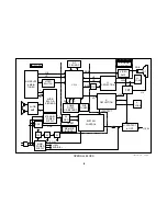
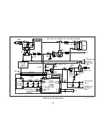
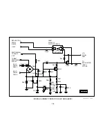
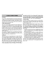
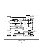
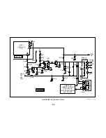
The power supply in the BA-5 chassis uses one switching IC to control
switching of the B+ through a transformer. The transformer primary couples
the signal to the secondary. The secondary signals are used to create
three DC voltages that are used to supply power to the rest of the set.
Feedback from the primary side of the transformer and the +135 volt line
created by the secondary is used to control the switching frequency. The
IC also has three built-in protection circuits.
Startup
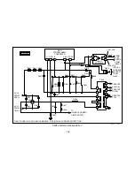
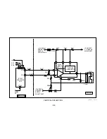
When power is turned ON, RY602 is closed and AC is applied to R637
and D605. The AC applied to R637 is passed through R662 and R660,
and applied to IC601/4 VIN. As C620 charges on the first positive half
cycle of the incoming AC signal, its voltage reaches the threshold at which
IC601 Converter will start to operate. This threshold is around 11 volts.
Once IC601 starts operating, the incoming AC will not be a factor in sus-
taining the charge of C620. The voltage at IC601/4 VIN will remain at
approximately 17 VDC during normal operation due to a sustaining volt-
age, which will be created using the signal from T603/7.
When AC is applied to D605, 144 VDC is developed. This voltage is sent
through R626 to T603/5. When the voltage across C620 is sufficient to
allow IC601 to operate, current flows through T603/5 and T603/4, and
T603/3 and T603/2, through IC601/3 D and IC601/2 S, and finally through
R632 and R641 to ground. IC601/3 and 4 are the Drain and Source for an
internal FET. The gate of this internal FET is connected to an oscillator
contained in IC601 Converter. When the voltage threshold for startup is
reached at IC601/4 VIN, the oscillator begins operation by outputting its
positive half cycle. This turns the internal FET ON, allowing current to
flow as described above. When the oscillator starts its negative half cycle,
the FET is turned OFF and current stops flowing through T603/4 and 5
and T603/2 and 3.
This switching ON and OFF of the internal FET, whose Drain and Source
are IC601/3 and 2 respectively, produces a signal output at T603/7 that is
rectified by D613 and applied to IC601/4 VIN. The DC voltage produced
by D613 is used to sustain the input voltage at IC601/4 VIN.
When this sustaining voltage is missing, IC601 will begin to start up. With-
out this voltage, C620 will discharge on the negative half cycle of the
incoming AC. This causes the IC601 to be constantly turned ON and
OFF. A chirping noise accompanies this failure and the Standby/Timer
LED will flash. If the voltage supplied to IC601/4 VIN exceeds 22 volts,
the IC will go into internal over voltage shutdown and cease oscillation.
Regulation
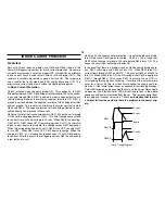
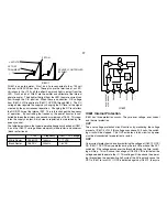
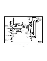
IC601 Converter is used here in quasi-resonant operation. Quasi-reso-
nant refers to the fact that there are two different levels used to determine
how long the internal FET of IC601 should be turned ON or OFF. The
resistance and capacitance values of the components associated with
IC601/1 and 2 determine this.
When the supply is started, the voltage created across R632 and R641
monitors the current through the internal FET. This voltage is fed to IC601/
1 through R633. This pin is connected internally to two internal compara-
tors. When this voltage reaches .73 volts, Comparator 1 in IC601 Con-
verter turns the internal FET OFF. When this occurs, a positive going
signal is produced at T603/7 due to the collapsing magnetic field. This
signal is rectified by D614. The rectified voltage is delayed by the charg-
ing action of C652. The delay time is a factor of the values of R646, R643
and C652. The rectified and delayed voltage from D614 is then sent
through D611, blocking diode, to IC601/1 OCP/FB. When this voltage
reaches approximately 4 volts, Comparator 2 in IC601 turns the FET ON.
This causes a loss of the D614 voltage due to the changes in magnetic
field of T605. The voltage across R632 and R641 will increase again and
the cycle repeats itself.
Summary of Contents for FD TRINITRON WEGA KV-13FM12
Page 27: ...22 NOTES ...
Page 48: ...APPENDIX ...

