i
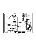
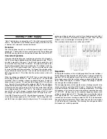
Q621/D - 50 mv, 10 us
Q621/G - 1 V, 10 us
Q621/S - 1 V, 10 us
Standby Power Supply
*Note: The following is an excerpt from CTV-26, which covered the AA2W
chassis. The operation of the Standby Power Supply in the BA-5 chassis
is identical, but component names are different.
Overview
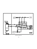
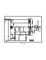
The standby power supply is a switching power supply used to create
Standby 5V. The Standby 5V line is used to power the Tuning Micon and
EEPROM and any other circuits which need power when the set is OFF.
Converter Operation
Operation of the Standby power supply begins when the set is plugged in.
The AC line voltage is applied across the standby power supply. The AC
low side is ground for this circuit. The AC high side is applied to a half
wave rectifier consisting of D621 and D622. Two diodes are used so that
there will be protection should one of them fail. This voltage is then ap-
plied to T621/1 SRT Input through R639. R639 is a fusible resistor used
for current limiting and failure protection. It will open if the standby switch-
ing circuit draws excessive current. Please note that the board has T621
SBT silk-screened on it. This differs from the service manual, which calls
T621 SRT.
When the voltage is applied to T621/1 SRT Input, current flows through
the winding and R631 to Q621/G. Q621 Converter is a FET with added
protection. When a positive voltage is applied to the gate, it begins to
conduct drain to source. This reduces the voltage at T621/3 to close to
zero. Normally this would reduce the voltage at Q621/G, but a voltage is
supplied to the gate through R632 and C630 from T621/4. This voltage is
induced into the secondary winding of T621/4 when current flows through
the winding between T621/1 and T621/3. The voltage is not permanent
due to C630. As C630 charges, it reduces the voltage at Q621/G. Once
this voltage falls below a certain threshold, Q621 Converter turns OFF.
Once Q621 Converter turns OFF, all polarities are reversed. This rever-
sal of polarity helps speed up turn OFF of Q621. D623, along with C631
and R640, form a snubber network (voltage clamp). This network clamps
excessive voltage overshoot caused by the collapsing magnetic field of
T621 SRT and returns the excessive voltage to C629. When the field
collapses fully, current begins to flow through T621/1 and 3.
The waveforms below show what will be seen at Q621.
Regulation
Changing the frequency of the switching regulates the output voltage at
the secondary winding comprised of T621/8 and 9. Taking a sample volt-
age from T621/4 and applying it to rectifiers D624 and D625 does this. As
this voltage rises and falls, the rectified voltage is applied to Q622/B through
R634. When Q622 begins to conduct, it lowers the voltage at Q621/G
and changes the switching frequency.
The changing frequency will change the amount of voltage coupled to the
secondary winding consisting of T621/8 and 9. If the load on the second-
ary output increases, the frequency of switching will decrease. This brings
the frequency of the converter closer to the optimum operating frequency
of T621 SRT. Moving closer to this optimum frequency causes more
voltage to be provided at T621/9. The opposite occurs when the load on
the supply decreases. This causes the frequency of operation to be in-
creased and the amount of voltage coupled to T621/9 to be decreased.
The supply typically operates at 45 kHz when the set is OFF and at about
30 kHz when the set is operating. The incoming line voltage also effects
the frequency of switching operation.
Summary of Contents for FD TRINITRON WEGA KV-13FM12
Page 27: ...22 NOTES ...
Page 48: ...APPENDIX ...

