background image

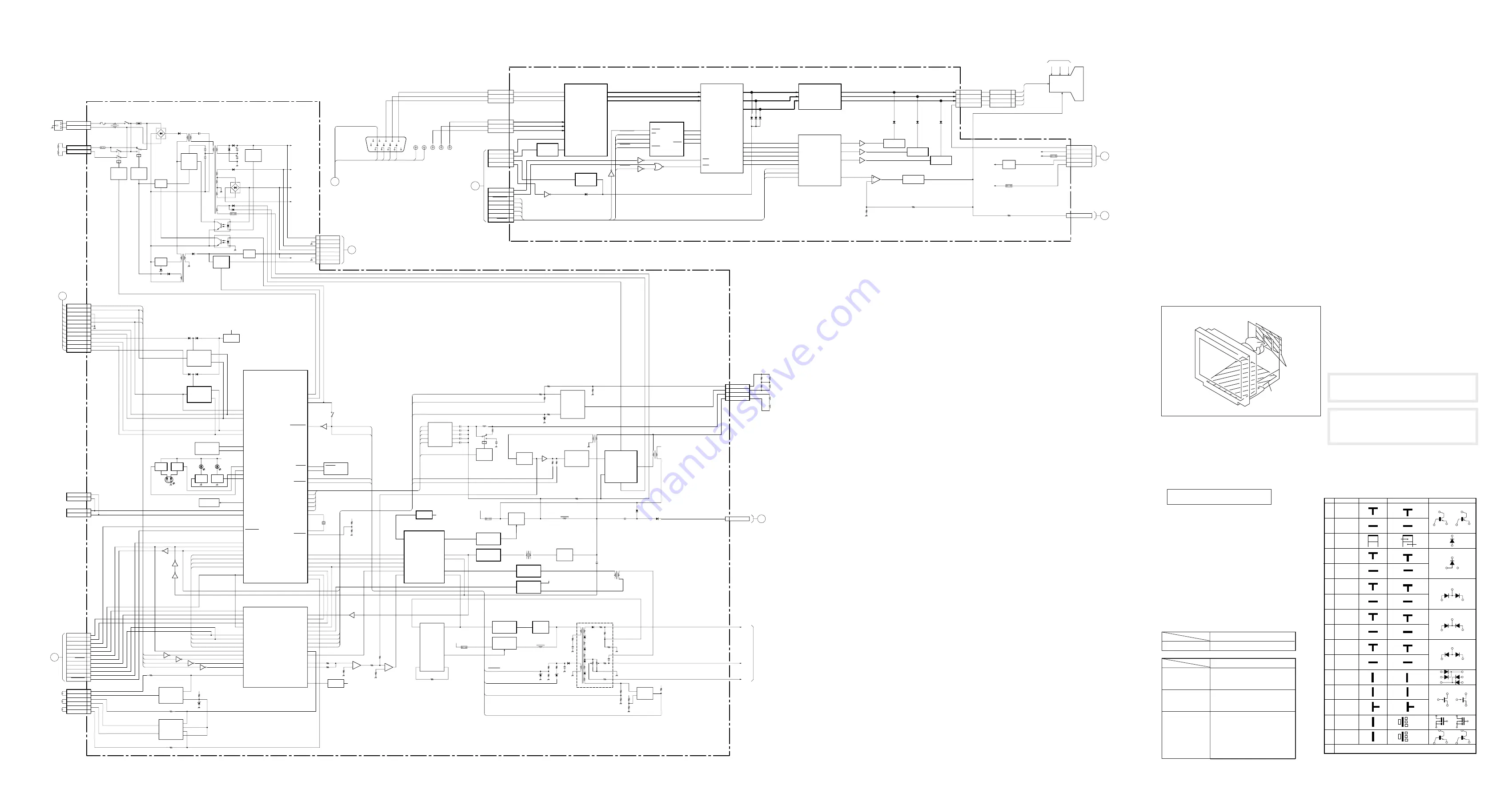
5-1. BLOCK  DIAGRAMS  (with  FRAME  SCHEMATIC  DIAGRAM)

SECTION  5

DIAGRAMS

5-1

5-2

5-3

5-4

5-2. CIRCUIT  BOARDS  LOCATION

G

D

S

2

3

4

5

6

7

8

9

0

!™

1

G

D

S

G

S

S

D

G

D

Ver.1.5

Transistor
(FET)

Transistor

Transistor

Discrete semiconductot

(Chip semiconductors that are not actually used are included.)

Diode

Diode

Diode

Diode

Diode

Diode

Diode

Diode

Diode

Diode

Source

Source

Anode

Anode

(NC)

(NC)

Cathode

Anode

Cathode

Common

Cathode

Cathode

Common

Cathode

Cathode

Common

Common

Common

Common

Cathode

Anode

Base

Emitter

Collector

Base

Emitter

Collector

Drain

Gate

Gate

Drain

Device

Printed symbol

Terminal name

Circuit

Terminal name of semiconductors in silk screen

printed circuit (    )

Anode

Anode

Anode

Cathode

Anode

Anode

Cathode

Transistor
(FET)

Transistor
(FET)

!∞

Emitter

Collector

Base

Transistor

Source

Gate

Drain

Cathode

Anode

Anode

Cathode

Anode

Anode

*

• All voltages are in V.

• Readings are taken with a 10 M  digital multimeter.

• Readings are taken with a color-bar signal input.

• Voltage variations may be noted due to normal production

tolerances.

*

: Can not be measured.

• Circled numbers are waveform references.

s

: B + bus.

S

: B – bus.

Note: The components identified by shading and mark

¡

 are critical for safety. Replace only with part

number specified.

Note: Les composants identifiés par un tramé et une

marque 

¡

 sont critiques pour la sécurité. Ne les

remplacer que par une pièce portant le numéro
sp

é

cifié.

5-3. SCHEMATIC  DIAGRAMS  AND

PRINTED  WIRING  BOARDS

Note:

• All capacitors are in µF unless otherwise noted. (pF:  µµF)

Capacitors without voltage indication are all 50 V.

• Indication of resistance, which does not have one for rating

electrical power, is as follows.

Pitch: 5 mm

Rating electrical power 1/4 W (CHIP : 1/10 W)

• All resistors are in ohms.

f

: nonflammable resistor.

Ï

: fusible resistor.

¢

: internal component.

p

: panel designation, and adjustment for repair.

• All variable and adjustable resistors have characteristic curve B,

unless otherwise noted.

e

: earth-ground.

E

: earth-chassis.

• The components identified by 

[

 in this basic schematic diagram

have been carefully factory-selected for each set in order to

satisfy regulations regarding X-ray radiation.

Should replacement be required, replace only with the value

originally used.

• When replacing components identified by 

]

, make the

necessary adjustments indicated. (See page 3-1)

• When replacing the part in below table, be sure to perform the

related adjustment.

HV ADJ

Part replaced ( 

[

 )

RV901

HV Regulator
Circuit

HV HOLD DOWN
Circuit

Beam Current
Protector Circuit

Part replaced ( 

]

 )

D board

IC901, R903, R922,
T901
• Mounted D board

D board

D913, D916, C923,
R920, R927, T901
• Mounted D board

D board

IC901, D902, D918,
D919, R923, R928,
R932, R933, R934,
R942, R944, R945,
R947, R948, R951,
T901
• Mounted D board

A

D

R IN 2

G IN 2

B IN 2

C.BLK

R IN 1

G IN 1

B IN 1

DAC_SEL

5

4

3

2

1

10

9

8

7

6

15

14

13

12

11

HD15

VD

HD

B

G

R

5BNC

1

3

6

1

3

5

R_IN2

G_IN2

B_IN2

R_IN1

G_IN1

B_IN1

SW

G.SYNC

R_OUT

G_OUT

B_OUT

MOSI

CLK

HFLB

SS

VFLB

OSD_SEL

7

5

2

16

13

11

19

25

27

30

35

5

6

7

8

22

IC404

OSD

R

G

B

FBKG

27

26

25

24

R_IN

G_IN

B_IN

R_OSD

G_OSD

B_OSD

OSD_BLK

RGB DRIVE

R_DRV

G_DRV

B_DRV

OSD CONT

R_OUT

G_OUT

B_OUT

DAC_SEL

R_IN

G_IN

B_IN

R_OUT

G_OUT

B_OUT

KR

KG

KB

)

KR

KG

KB

)

)

+15V

CN405

A

(VIDEO AMP,RGB OUT)

BRT

RGB OUT

D/A CONVERTER

R_DRV

G_DRV

B_DRV

BRT

CONT

OSDCONT

LD

CLK

MOSI

R_CUTOFF

G_CUTOFF

B_CUTOFF

6

7

8

9

12

13

15

16

17

3

4

5

V901

PICTURE TUBE

FV1

FV2

HV

TO FBT

G2

1

1KV

IC406

12V REG

O

I

+12V

+5V

+80V

+80V

G.SYNC

VIDEO OUT

G2 CONT

R_CUTOFF

G_CUTOFF

B_CUTOFF

+180V

1

7

5

4

3

CN405

CN407

CN408

8

6

4

2

8

6

4

2

Q101,102

Q201,202

Q301,302

IC405(1/4)

IC405(2/4)

IC405(3/4)

IC405(4/4)

19

G2

IC401

IC407

18

20

23

26

27

28

25

13

14

DMP_CLK

DMP_DATA

CONT

CLP

BLK

16

15

4

1

2

3

5

8

11

DAMP_DATA

DAMP_CLK

V BLK

IC408

RGB INPUT SELECT

V BLK

Q402

Q401

CN404

CN403

IC402(1/4)

IC402(2/4)

IC402(3/4)

IC402(4/4)

V.BLK

DAMP_CLK

DAMP_DATA

OSD_SEL

S/C ENABLE

AUTO S/C

CLAMP

INPUT_SEL

STBY 5V

Q409,Q410

IC403

Q404~Q406

B-SS3420<U/C>-B/D-P1

8

9

11

5

3

1

+180V

C

D

NOR

H BLK

SYNC ONG

A

5

1

CN401

3

4

1

4

9

7

6

8

2

3

B

CN402

H.BLK

4

3

-

+

+15V

CURRENT AMP

9

11

1

8

10

2

IC013

VS1

CS1

VS2

CS2

DMP CLK

DMP DO

DMP DI

DMP ID

39

38

46

7

45

9

11

10

12

6

41

43

42

44

33

IC007

CLP OUT

CBLK OUT

SONG

VIDEO

INPUT_SEL

CLK

DO

DI

ID

FBPIN

HS/CS1

VS1

HS/CS2

VS2

TILT

HTIM

VIDEO OUT

VS OUT

HS OUT

VDF

HCENT

H SHAPE BAL

V SHAPE

VDC

MOIRE

H SHAPE

H SIZE

2

8

48

47

28

32

29

19

26

34

30

31

DMP CLK

DMP DO

DMP DI

DMP ID

9

16

10

60

65

21

22

24

17

79

20

19

RXD

TXD

2

1

IC009

12

13

34

EEP SDA

EEP SCL

IC004

EEP ROM

5

6

25

26

V CLK

SDA

SCL

V CLK

SDA

SCL

IC012

ROM

IC002

ROM

47

30

31

32

33

7

7

5

6

5

6

CPU

IC001

CS1

VS1

CS2

VS2

P70/IRQ0

DDC_SDA_1

DDC_SCL_1

DDC_SDA_2

DDC_SCL_2

KEY_DET

EEP_SDA

EEP_SCL

LED0

LED1

TXD

RXD

ASC SW

OSD_SEL

DAC SEL

HFBP

VRET

DMP_CLK

DMP_DO

DMP_DI

DMP_ID

INPUT SEL

66

59

29

28

41

63,64

4

9

10

7

14

AFC1

SDA

SCL

HSYNC

MOIRE

PWM RFE

DF OUT

HVD OUT

HD OUT

FBP

PMW OUT

IC010

SYNC PROCESS

17

24

25

19

23

6

5

7

2

3

1

H DRIVE

PIN DRIVE

PROT DET

DGC

HTR SW

POWER SW

100

99

98

96

CK

RESET

8

3

IC005

WDT

85

86

87

88

89

90

82

83

X001

HV_PROT

VDC

VRET

I

O

5V REG

RY501

S0

S1

S2

S3

S4

S5

H OUT

PS501

H DF OUT

V DF OUT

IC901

HV CONTROL

1

19

7

HV DRIVE

HV OUT

HRC

HV REG SW

PS901

12

8

ABL_DET

HV_DET

T902

FBT

HV

FV1

FV2

TO PICTURE TUBE

3

V OUT

H CENT

CONTROL

H CENT

H SHAPBAL

2

1

-VIN

+VIN

VEE

OUT

VCC

4

5

3

IC502

H CENT OUT

1KV

V.DY C

V.DY H

H.DY C

DPU

43

77

78

38

93

WDT

RESET

ABL DET

HV DET

S0

S1

S2

S3

S4

S5

XTAL0

XTAL1

+B DET

HPLL

IIC SDA

IIC SCL

HS

VS

ASC

HST

DFT

1

V.DY

H.DY

H.DY H

PIN AMP

PIN OUT

S CAP

CHANGE

RELAY

DRIVE

1

3

1

4

AC L

AC N

DGC

DGC

DGC

AC INLET

V SHAPE

CN601

T501

HDT

HOC

F601

6.3A

T601

D601

TH601

THP601

RY601

RY602

RELAY

DRIVE

Q605

RELAY

DRIVE

Q601

VCC SW

Q602

REG OUT

IC603

+180V

REG

IC604

REG SW

IC602

REG

HEATER

IC601

PH601

PH602

T603

+180V

+80V

+15V

-15V

1

2

3

4

5

6

7

CN504

+180V

GND

+80V

+15V

STBY5V

GND

HEATER

CN501

+180V

IC501

14

15

LED2

LED3

1

2

CN509

6

5

4

3

8

8

VCC

VCC

Q003

Q004

Q005

Q001

STBY+5V

S001~S008

HOST+5_2

DDC_SCL_2

DDC_SDA_2

HOST+5_1

DDC_SCL_1

DDC_SDA_1

GND

V.SYNC-2

C.SYNC-2

GND

1

2

3

4

5

6

7

8

9

10

11

12

CN502

Q002

5V REG

+15V

OUT

IC1501

1

2

3

4

5

6

CN507

ROTATION(-)

RO)

IC1502

OUT

OUT

-

+

-

+

V CONV

27

74

H CONV

1

3

4

5

6

7

8

9

11

12

13

14

CN503

AUTO S/C

S/C ENABLE

SYNC ON G

INPUT_SEL

CLAMP

H BLK

V BLK

C BLK

DMP_CLK

DMP_DATA

DAC_SEL

OSD_SEL

IC011

9V REG

+15V

+9V

PWM OUT

H VD IN

+

-

+180V

Q901,Q903,Q904

Q906

T902

Q905

Q505,Q511

Q530,Q531

T502

-

+

O

4MHz

IC902

ABL PROT

2

+9V

HV_PROT

+15V

9V REG

+15V

IC008

Q519

T503

Q503,Q504,Q512

Q516,Q528,Q529

Q507,Q509,Q510

T505

HCT

+300V

CN505

L504

HLC

Q527

Q518,Q520

Q522,Q523,Q524

Q525

Q521

Q517

T504

5

OUT

IC605

1

-

3

2

4

6

CN506

D

(POWER SUPPLY,U-COM,DEFLECTION)

B-SS3420<U/C>-B/D-P2

T602

D617

USB_TX

USB_RX

USER CONT

LED DRIVE

LED DRIVE

LED DRIVE

LED DRIVE

3

7

6

Q008

+180V

Q514

IC1504

H SIZEFB

D

+300V

27

3

1

ABL_PROT

ABL_PROT

Q603

Q604

3

4

4

V.STAT+

V.STAT-

H.STAT+

H.STAT-

B

STBY5V

C

SW601

POWER

SWITCH

T604

C.SYNC_1

V.SYNC_1

A

Summary of Contents for GDM-200PS

Page 1: ...m w h 11 5 8 9 1 4 inches Deflection frequency Horizontal 30 to 92 kHz Vertical 48 to 160 Hz AC input voltage current 100 to 240 V 50 60 Hz 1 7 1 0 A Power consumption Max 120 W Dimensions 406 432 420 mm w h d 16 17 1 8 16 5 8 inches Mass Approx 18 8 kg 41 lb 7 oz Supplied accessories See page 6 Design and specifications are subject to change without notice TRINITRON COLOR GRAPHIC DISPLAY GDM 200P...

Page 2: ... DEGAUSS COIL HAS BEEN REMOVED SAFETY RELATED COMPONENT WARNING COMPONENTS IDENTIFIED BY SHADING AND MARK ON THE SCHEMATIC DIAGRAMS EXPLODED VIEWS AND IN THE PARTS LIST ARE CRITICAL FOR SAFE OPERATION REPLACE THESE COMPONENTS WITH SONY PARTS WHOSE PART NUMBERS APPEAR AS SHOWN IN THIS MANUAL OR IN SUPPLEMENTS PUBLISHED BY SONY CIRCUIT ADJUSTMENTS THAT ARE CRITICAL FOR SAFE OPERATION ARE IDENTIFIED ...

Page 3: ...Amber Off 1 5 sec 0 5 sec Amber Off 0 5 sec 1 5 sec Amber Off Amber Off 0 25 sec 0 5 sec 0 25 sec 1 25 sec Amber Off Green Off 0 5 sec 0 5 sec 0 5 sec 0 5 sec Aging Mode Video Aging During Power Save press MENU key for longer than 2 second Self Test OSD Color Bar During Power Save press CONTRAST key for longer than 2 second Reliability Check Mode During Power Save press CONTRAST key for longer tha...

Page 4: ...moval 2 2 2 5 Service Position 2 2 2 6 Picture Tube Removal 2 3 3 SAFETY RELATED ADJUSTMENT 3 1 4 ADJUSTMENTS 4 1 5 DIAGRAMS 5 1 Block Diagram with Frame Schematic Diagram 5 1 5 2 Circuit Boards Location 5 4 5 3 Schematic Diagrams and Printed Wiring Boards 5 4 1 Schematic Diagram of D Board 5 5 2 Schematic Diagram of A Board 5 13 5 4 Semiconductors 5 16 6 EXPLODED VIEWS 6 1 7 ELECTRICAL PARTS LIST...

Page 5: ...Getting Started Getting Started F EN ES C Identifying Parts and Controls See the pages in parentheses for further details Front 1 RESET reset button page 17 Resets the adjustments to the factory settings 2 ASC auto sizing and centering button page 7 Automatically adjusts the size and centering of the images 3 INPUT input button and HD15 BNC indicators page 8 Selects the HD15 or 5BNC video input si...

Page 6: ...ing an item the bar length and the figure increase or decrease When setting an item the p mark turns green MENU MENU EXIT CENTER SIZE GEOM COLOR LANG ZOOM SCREEN OPTION OK MENU MENU MENU 11 Getting Started Customizing Your Monitor F EN ES C Using the CENTER On screen Display The CENTER settings allow you to adjust the centering of the picture Once the setting is adjusted it will be stored in memor...

Page 7: ...ce the setting is adjusted it will be stored in memory for the current input signal 1 Press the MENU button The MENU OSD appears 2 Press the and buttons to select ZOOM and press the MENU button again The ZOOM OSD appears 3 Press the buttons to adjust the picture zoom to enlarge the picture to reduce the picture The OSD automatically disappears after about 30 seconds To close the OSD press the MENU...

Page 8: ...ows down to shift red shadows down and blue shadows up to turn CANCEL MOIRE ON to turn CANCEL MOIRE OFF to increase the moire cancellation effect to decrease the moire cancellation effect MENU SCREEN TOP BOT H CONVERGENCE 26 ON OFF ON OFF 50 0 15 Getting Started Customizing Your Monitor F EN ES C Using the OPTION On screen Display The OPTION OSD allows you to manually degauss the screen and adjust...

Page 9: ...K 1 MIN OPTION ZZ MENU ON MANUAL DEGAUSS UNLOCK 1 MIN OPTION ZZ ZZ PWR SAVE DELAY OPTION 5 SEC 60 MIN 1 MIN OFF AUTO ZZ CONTROL LOCK OPTION UNLOCK LOCK AUTO 17 Getting Started Customizing Your Monitor F EN ES C Using the LANG Language On screen Display English French German Spanish and Japanese versions of the OSDs are available 1 Press the MENU button The MENU OSD appears 2 Press the and buttons ...

Page 10: ...monitor with the buttons on the front panel White does not look white Screen image is not centered or sized properly Edges of the image are curved White lines show red or blue shadows at edges Picture is fuzzy Picture bounces or has wavy oscillations Pictureisflickering Picture appears to be ghosting Wavy or elliptical moire pattern is visible Two fine horizontal lines wires are visible Hum is hea...

Page 11: ...BLY 2 1 CABINET REMOVAL 2 2 A BOARD REMOVAL 2 1 Eight screws BVTT 3 x 8 6 Two claws 2 EMI shield 7 Video shield 5 Cabinet 3 Two screws BVTP 4 x 16 1 Four screws BVTT 3 x 8 4 CN406 CN405 CN404 CN403 CN401 CN402 A board 2 Three screws BVTT 3 x 8 1 ...

Page 12: ...s to fix 2 2 CN404 CN403 CN601 AC inlet 3P 6 Two screws Ext tooth washer screw M4 2 Two screws BVTT 3 x 8 7 Two screws KTP 3 x 8 5 Rear shield 3 I O terminal board 8 Screw Ext tooth washer screw M4 4 A board 1 GND GND Connector 9pin CN602 Shield plate 2 D board 5 Three screws BVTP 3 x 10 3 Screw BVTT 4 x 8 1 Printed circuit board holder 4 CN601 D board AC inlet 3P ...

Page 13: ...ut or hurt the rubber a b c Anode Button REMOVAL OF ANODE CAP NOTE Short circuit the anode of the picture tube and the anode cap to the metal chassis CRT shield or carbon painted on the CRT after removing the anode REMOVING PROCEDURES 1 Turn up one side of the rubber cap in the direction indicated by the arrow a 2 Using a thumb pull up the rubber cap firmly in the direction indicated by the arrow ...

Page 14: ...f C639 and GND Connect a variable resistor 20 kΩ or more and an ammeter in series between FBT pin and 15 V line side of C637 Decrease gradually the resistance of the variable resistor form maximum to minimum and confirm that the Beam Current Protector Circuite works TV Raster disappears The current must be within the range shown below Standard current Less than 1 14 mA HV Regulator Circuit HV HOLD...

Page 15: ...e CRT surface 7 With landing checker adjsut DY position punity DY tilt DY center and landing of hte 4 corners Purity Adjsutment use 2 pole Mg on DY side 8 Fasten DY with screw Note Torque 22 2kg cm 2 2 0 2 Nm Perform auto degaussing A difference between red and blue must be within the specification given right Adjustment and measurement should be made at the points one inch inside the fluorescent ...

Page 16: ... Fig 1 3 Make rough adjustment of the H and V direction conver gence by using 4 fold poles magnet Convergence Specification White Balance Adjustment Specification 1 9300K x 0 283 0 005 y 0 298 0 005 All White 2 6500K x 0 313 0 005 y 0 329 0 005 All White Vertical and Horizontal Position and Size Specification Focus adjustment Adjust the focus volume 1 and 2 for the optimum focus Standard HMC VMC 0...

Page 17: ...CTURE TUBE FV1 FV2 HV TO FBT G2 1 1KV IC406 12V REG O I 12V 5V 80V 80V G SYNC VIDEO OUT G2 CONT R_CUTOFF G_CUTOFF B_CUTOFF 180V 1 7 5 4 3 CN405 CN407 CN408 8 6 4 2 8 6 4 2 Q101 102 Q201 202 Q301 302 IC405 1 4 IC405 2 4 IC405 3 4 IC405 4 4 19 G2 IC401 IC407 18 20 23 26 27 28 25 13 14 DMP_CLK DMP_DATA CONT CLP BLK 16 15 4 1 2 3 5 8 11 DAMP_DATA DAMP_CLK V BLK IC408 RGB INPUT SELECT V BLK Q402 Q401 C...

Page 18: ...7 0 047 B CHIP 33 200V HR 0 22 100V PT 0 33 200V PP 1000p B CHIP 100 25V 0 047 200V PT 2200p B CHIP 330p B CHIP 47 25V 0 1 PT 47 25V 100p CH CHIP 1000 25V 1000 25V 0 22 100V PT RD5 1ESB2 MA111 MA111 MA111 RD7 5ESB1 D2L40 TA MA111 SB340L RD5 1ESB2 RGP02 ERA91 02 MA111 RGP02 D1NS4 TR UF4005 RD12ESB2 RGP10G D2L40 RD24ESB2 RD12ESB2 MA111 MA111 MA111 RD16ESB2 EGP10G D2L40 TA RD5 1ESB2 RD5 1ESB2 1SS119 ...

Page 19: ...5 9 5 10 D POWER SUPPLY U COM DEFLECTION D BOARD Conductor Side D BOARD Component Side 1 2 3 4 5 A B C D E F G 1 2 3 4 5 A B C D E F G ...

Page 20: ...3 D106 C 2 3 D111 D 2 7 D201 D 1 6 D203 B 1 B 2 D204 B 1 B 2 D205 B 2 3 D206 C 2 3 D211 D 2 7 D301 D 1 6 D303 B 1 B 2 D304 B 1 B 2 D305 B 2 3 D306 C 2 3 D311 D 2 7 D401 D 3 D 1 D406 D 2 D 2 D413 A 2 A 1 D414 A 2 A 1 D415 A 1 A 2 Conductor Side Conductor Side Conductor Side Refer to Terminal name of semiconductors in silk screen printed circuit see page 5 4 A BOARD Component Side 1 2 3 A B C D 1 2 ...

Page 21: ...5LL560 BK2125LL560 BK2125LL560 1 1UH 1 1UH 1 1UH 1 1UH 1 1UH 100µH 100µH 1A 2SC4015 G CUTOFF AMP 2SC4015 B CUTOFF AMP 2SA1037K 2SC5022 02 G2 AMP 10 CHIP 56 CHIP 2 2M CHIP 390 CHIP 39k CHIP 1M CHIP 2 2k CHIP 100k CHIP 1k CHIP 100k CHIP 2 2k RN CP 2 2M CHIP 22 CHIP 100k CHIP 100k CHIP 10 CHIP 2 2M CHIP 390 CHIP 2 2k CHIP 1k CHIP 100k CHIP 1k CHIP 39k CHIP 2 2k RN CP 2 2M CHIP 22 CHIP 100k CHIP 100k ...

Page 22: ...EKA T146 2SA1036K Q 2SA1036K T 146 Q 2SA1037K T 146 QR 2SC1623 L5L6 2SC2412K T 146 QR DTA124ESA 2SC2459 GR 2SC2784 2SC2785 HFE 2SC3311A RTA IRLI530GLF33 IRLI540GLF33 IRFPE50LF21 2SA1049 GR 2SA1091 O 2SC2362K G 2SA1358 Y 2SC3421 Y 2SC2362KG AA 1 TOP VIEW n 8 pin SOP 1 TOP VIEW n 20 pin SOP 1 TOP VIEW n 48 pin QFP 1 TOP VIEW n 28 pin SOP MARKING SIDE VIEW 1 5 pin SIP 5 1 10 1 1 TOP VIEW n 28 pin DIP...

Page 23: ...20U EL1Z ERA22 06AVRBT ERA22 08 GP08D GP08DPKG23 HSS83TD RPG02 17EL 6433 RPG02 17PKG23 RGP10GPKG23 UF4005PKG23 D2L40 TA D4SBS4 D4SBS4 F D4SB60L D2S4MF D2S4MTA1 D5L60 FMQ G5FMS PG124S15 EGP10D ERA91 02 RGP10JPKG23 S2LA20F MA151WK 1SS184 PC123F2 PC123FY2 P6KE170AG23 SB340L 6489 RD7 5M B2 SB340 1PS226 115 1SS376TE 17 SEL1922D C SEL1922D C D SPB 26MVWF E C B E C B B C E E C B CATHODE ANODE CATHODE ANO...

Page 24: ... PART NO DESCRIPTION REMARK 1 X 4034 844 1 SHIELD ASSY EMI U C SH model 1 X 4035 398 1 SHIELD ASSY EMI AEP UK model 3 4 394 972 21 CAP POWER 4 A 1346 713 B D BOARD COMPLETE 5 5 X 4035 177 1 TRANSFORMER ASSY FLYBACK NX 4401 J1M4 6 1 694 347 11 TERMINAL BOARD ASSY I O 7 4 389 025 01 SCREW M4 EXT TOOTH WASHER 8 1 251 382 22 INLET AC 3P WITH NOISE FILTE 9 4 052 345 01 SCREW 3X8 K TAPPING 10 4 060 368 ...

Page 25: ...16 01 SPRING EXTENSION except U C for USA made set 60 4 061 573 01 SPRING TENSION U C for USA made set 61 1 416 282 41 COIL DEMAGNETIC 62 4 056 260 01 SPACER DEGAUSSER COIL 63 4 203 648 01 SCREW 5 SELF TAPPING AEP UK model 63 4 365 808 01 SCREW 5 TAPPING U C SH model 65 4 389 025 01 SCREW M4 EXT TOOTH WASHER 66 4 382 848 01 HOLDER PRINTED CIRCUIT BOARD 67 3 703 141 00 HOLDER PRINTED CIRCUIT BOARD ...

Page 26: ...00PST9 105 1 759 641 21 DISK INFORMATION WINDOWS 3 5 U C for USA made set 105 1 759 641 14 DISK INFORMATION WINDOWS 3 5 except U C for USA made set 106 4 060 582 01 CUSHION UPPER ASSY AEP UK model 106 4 060 574 01 CUSHION UPPER ASSY U C for USA made set 106 4 060 006 01 CUSHION UPPER ASSY U C for Japan made set SH model 107 4 041 927 11 BAG POLYETHYLENE U C SH model 107 4 060 490 01 BAG POLYETHYLE...

Page 27: ... 164 004 11 CERAMIC CHIP 0 1µF 10 25V C306 1 164 232 11 CERAMIC CHIP 0 01µF 10 50V C307 1 107 649 11 ELECT 2 2µF 20 250V C309 1 117 450 11 FILM 0 47µF 10 250V C320 1 104 664 11 ELECT 47µF 20 25V C324 1 163 263 11 CERAMIC CHIP 330pF 5 50V C330 1 115 340 11 CERAMIC CHIP 0 22µF 10 25V C352 1 104 664 11 ELECT 47µF 20 25V C401 1 164 232 11 CERAMIC CHIP 0 01µF 10 50V C402 1 164 232 11 CERAMIC CHIP 0 01µ...

Page 28: ... LM1283N IC404 8 759 566 26 IC LSC4380DW2AR2 IC405 8 759 502 82 IC LM324M IC406 8 759 263 43 IC TA78M12S IC407 8 759 435 33 IC LM2405T IC408 8 759 522 86 IC M52755FP TP JACK J401 1 251 598 11 SOCKET PICTURE TUBE COIL L401 1 412 537 31 INDUCTOR 100µH L402 1 408 615 31 INDUCTOR 100µH L404 1 414 189 31 INDUCTOR 100µH IC LINK PS401 1 533 590 31LINK IC 1A 90V AC 60V DC PS402 1 532 637 91LINK IC 1A 150V...

Page 29: ...P 2 2K 0 50 1 10W R332 1 216 129 00 RES CHIP 2 2M 5 1 10W R340 1 216 017 91 RES CHIP 47 5 1 10W R341 1 216 009 91 RES CHIP 22 5 1 10W R361 1 215 395 00 METAL 82 1 1 4W R363 1 216 017 91 RES CHIP 47 5 1 10W R371 1 216 097 00 RES CHIP 100K 5 1 10W R372 1 216 097 00 RES CHIP 100K 5 1 10W R401 1 216 057 00 RES CHIP 2 2K 5 1 10W R402 1 216 097 00 RES CHIP 100K 5 1 10W R403 1 216 089 00 RES CHIP 47K 5 1...

Page 30: ...ERAMIC CHIP 680pF 5 50V C041 1 164 004 11 CERAMIC CHIP 0 1µF 10 25V C042 1 164 004 11 CERAMIC CHIP 0 1µF 10 25V C043 1 164 004 11 CERAMIC CHIP 0 1µF 10 25V C044 1 164 004 11 CERAMIC CHIP 0 1µF 10 25V C045 1 104 760 11 CERAMIC CHIP 0 047µF 10 50V C046 1 104 760 11 CERAMIC CHIP 0 047µF 10 50V C047 1 104 760 11 CERAMIC CHIP 0 047µF 10 50V C048 1 163 017 00 CERAMIC CHIP 0 0047µF 10 50V C049 1 104 760 ...

Page 31: ...113 481 11 FILM 1000pF 5 630V C571 1 164 004 11 CERAMIC CHIP 0 1µF 10 25V C601 1 117 697 51 CERAMIC 470pF 10 250V C602 1 113 513 11 FILM 1µF 20 250V C603 1 115 166 11 FILM 0 22µF 20 250V C604 1 113 942 91 CERAMIC 0 0047µF 250V C605 1 117 697 51 CERAMIC 470pF 10 250V C606 1 113 942 91 CERAMIC 0 0047µF 250V C607 1 137 479 11 FILM 1µF 10 400V C608 1 117 849 11 ELECT 330µF 20 450V C609 1 117 971 51 MY...

Page 32: ...9 109 85 ZENER DIODE RD5 1ESB2 D003 8 719 045 19 DIODE SPB 26MVWF D005 8 719 109 85 ZENER DIODE RD5 1ESB2 D006 8 719 311 90 DIODE SEL1922D C D009 8 719 311 90 DIODE SEL1922D C D010 8 719 109 85 ZENER DIODE RD5 1ESB2 D011 8 719 976 99 ZENER DIODE DTZ5 1B D012 8 719 976 99 ZENER DIODE DTZ5 1B D013 8 719 106 23 ZENER DIODE RD7 5M B2 D014 8 719 404 50 DIODE MA111 TX D017 8 719 404 50 DIODE MA111 TX D0...

Page 33: ...C601 8 749 013 76 IC PQ6RD83B IC602 8 759 469 10 IC TOP223PF1 IC603 8 749 013 78 IC MCR5102 IC604 8 749 012 49 IC DM 57N IC605 8 759 231 53 IC TA7805S IC901 8 759 467 70 IC BA9756FS E2 IC902 8 759 510 73 IC BA10393F E2 IC1501 8 759 803 42 IC LA6500 FA IC1502 8 759 822 38 IC LA6510 IC1504 8 759 980 58 IC TDA8172 COIL L001 1 412 537 31 INDUCTOR 100µH L002 1 412 549 11 INDUCTOR 1mH L003 1 410 521 11 ...

Page 34: ...0 RES CHIP 1K 5 1 10W R032 1 216 049 00 RES CHIP 1K 5 1 10W R033 1 216 037 00 RES CHIP 330 5 1 10W R034 1 216 049 00 RES CHIP 1K 5 1 10W R035 1 216 671 11 METAL CHIP 6 8K 0 50 1 10W R036 1 216 073 00 RES CHIP 10K 5 1 10W R037 1 216 049 00 RES CHIP 1K 5 1 10W R038 1 216 049 00 RES CHIP 1K 5 1 10W R039 1 216 049 00 RES CHIP 1K 5 1 10W R040 1 216 037 00 RES CHIP 330 5 1 10W R042 1 216 073 00 RES CHIP...

Page 35: ...IP 1K 5 1 10W R552 1 216 081 00 RES CHIP 22K 5 1 10W R553 1 216 659 11 METAL CHIP 2 2K 0 50 1 10W R554 1 249 429 11 CARBON 10K 5 1 4W F R555 1 216 049 00 RES CHIP 1K 5 1 10W R556 1 216 073 00 RES CHIP 10K 5 1 10W R557 1 216 385 11 METAL OXIDE 0 47 5 3W F R558 1 216 097 00 RES CHIP 100K 5 1 10W R559 1 216 049 00 RES CHIP 1K 5 1 10W R560 1 260 096 11 CARBON 560 5 1 2W R561 1 249 413 11 CARBON 470 5 ...

Page 36: ...935 1 216 691 11 METAL CHIP 47K 0 50 1 10W R936 1 216 073 00 RES CHIP 10K 5 1 10W R937 1 216 025 00 RES CHIP 100 5 1 10W R938 1 216 089 00 RES CHIP 47K 5 1 10W R939 1 216 033 00 RES CHIP 220 5 1 10W R940 1 216 089 00 RES CHIP 47K 5 1 10W R942 1 216 669 11 METAL CHIP 5 6K 0 50 1 10W R943 1 216 065 00 RES CHIP 4 7K 5 1 10W R944 1 216 081 00 RES CHIP 22K 5 1 10W R945 1 216 081 00 RES CHIP 22K 5 1 10W...

Page 37: ... S003 1 571 532 21 SWITCH TACTILE OSD S004 1 571 532 21 SWITCH TACTILE BRT S005 1 571 532 21 SWITCH TACTILE BRT S006 1 571 532 21 SWITCH TACTILE INPUT S007 1 571 532 21 SWITCH TACTILE ASC S008 1 571 532 21 SWITCH TACTILE RESET SW601 1 571 433 31SWITCH PUSH AC POWER SPARK GAP SG901 1 519 422 11 GAP SPARK SG902 1 517 499 21 GAP SPARK TRANSFORMER T501 1 431 056 11 TRANSFORMER HORIZONTAL DRIVE T502 1 ...

Page 38: ... 48 GDM 200PS 200PST 200PST9 9 978 587 02 Sony Corporation Display Company Computer Display Dept GDM 200PS 200PST 200PST9 9 978 587 02 99DL05245 1 English 99DL05245 1 Printed in Japan 1999 4 ...

Reviews: