
- 1 -
E05728B67
Sony reserves the right to change products and specifications without prior notice. This information does not convey any license
by any implication or otherwise under any patents or other right. Application circuits shown, if any, are typical examples illustrating
the operation of the devices. Sony cannot assume responsibility for any problems arising out of the use of these circuits.
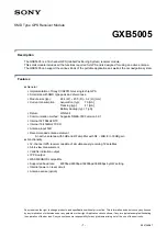
GXB5005
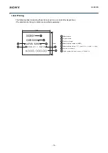
SMD Type GPS Receiver Module
Description
The GXB5005 is a 12-channel GPS (Global Positioning System) receiver module.
This small module includes all the functions required for GPS and is designed for using an active antenna.
The GXB5005 can support the various kinds of the portable applications as well as the car navigation system.
Features
General
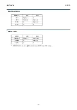
Implementation of Sony CXD2951GA-4 single chip GPS
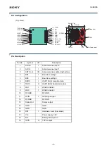
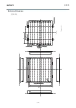
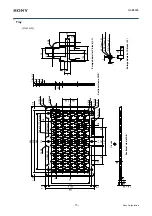
Small size with SMD type pads and shield case
Module size (typ.):
22.4 (W)
×
23.5 (D)
×
3.2 (H) [mm]
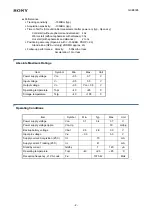
Current consumption:
Acquisition (typ):
70 [mA]
Tracking (typ):
41 [mA]
Battery backup (typ): 7 [
μ
A]
Datum:
WGS-84
Communication method: Supports NMEA-0183 version 3.01
Internal 32.768kHz RTC
Internal 18.414MHz TCXO
Antenna input 50
Ω
Recommended antenna element
An active antenna with 0dB and RF amplifier with NF
≤
2dB, 8 to 30dB gain
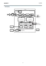
Functionality
12-channel GPS receiver capable of simultaneously receiving 12 satellites
All-in-view measurement
Valid fix indication output
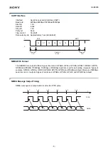
1PPS output
WAAS/EGNOS compatible
Supported baud rate:
4800bps/9600bps/19200bps/38400bps by HW setting
Internal power on reset circuit
Antenna sense (option)