background image

GXB5005

- 6 -

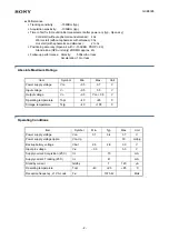
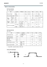
Electrical Characteristics


DC Characteristics

(Ta = –40 to +85

°

C)

AC Characteristics

(Ta = 25

°

C)

*1

Using SONY evaluation software “GPS View”

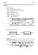
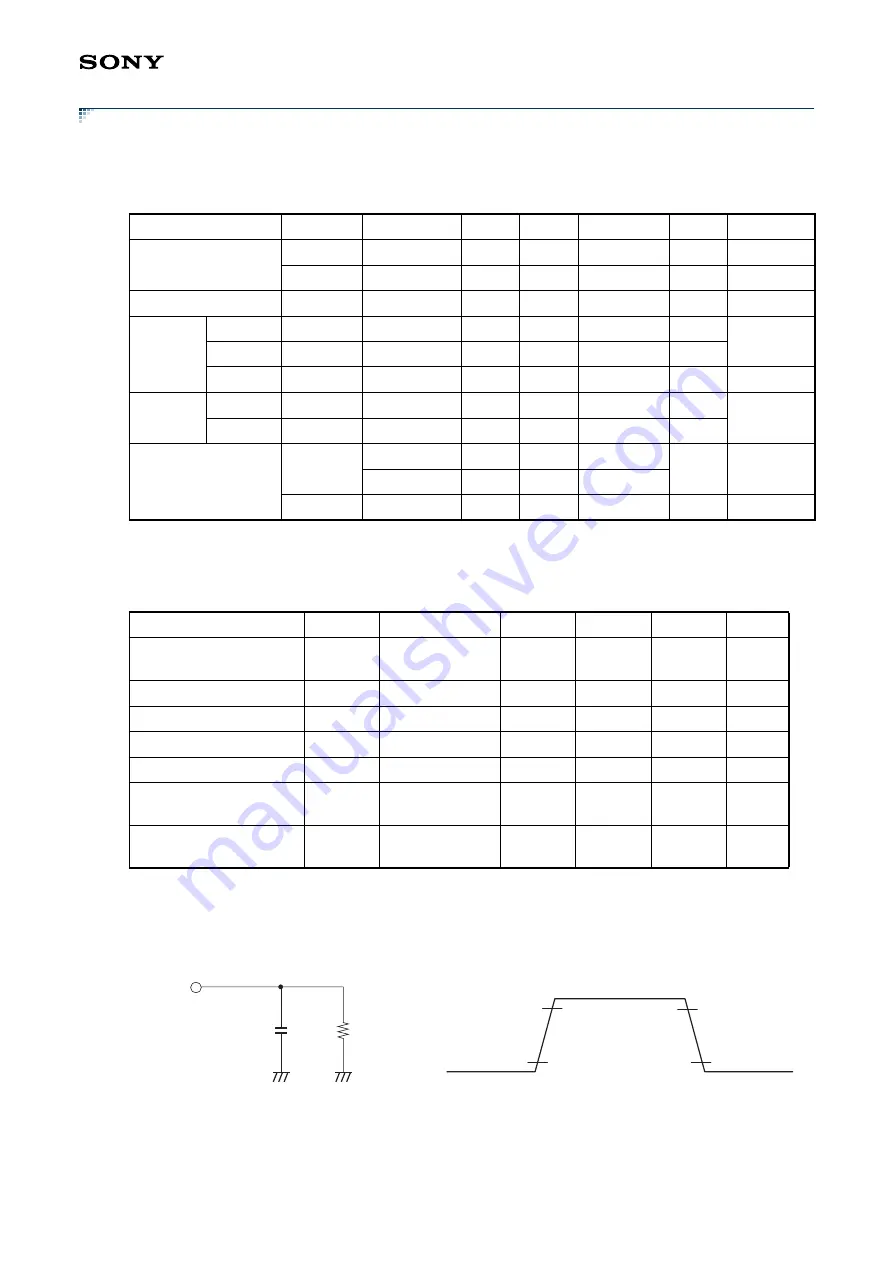
Timing of Output Signal

Item

Symbol

Condition

Min.

Typ.

Max.

Unit

Pins

Supply voltage

V

DD

3.1

3.4

3.7

V

17

Vbat

2.6

2.8

3.0

V

18

Supply voltage ripple

V

DD

-rip

50

mVp-p

17, 18

Input 
voltage 

H level

V

IH

2.0

5.5

V

3, 4, 5, 6, 8, 
9, 16

L level

V

IL

–0.3

0.8

V

AD

V

AD

0

(V

DD

 – 0.1)

V

1, 2

Output 
voltage

H level

V

OH

I

OH

 = –8mA

2.4

V

3, 7, 19

L level

V

OL

I

OL

 = 2mA

0.4

V

Current consumption

I

CC

 (3.3V)

Acquisition

70

mA

17

Tracking

41

Istdby

Vbatt = 2.8V

7

120

μ

A

18

Item

Symbol

Condition

Min.

Typ.

Max.

Unit

C/N output value

CN

–130dBm input, 
Tracking, 

*1

 42

 dB

TCXO frequency

Ftcxo

Internal

18.414

MHz

Message latency

Tl

1.0

s

RF gain

Grf

114

dB

Noise figure

NF

2

dB

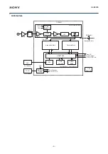
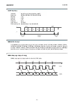
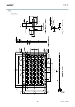
Output signal rise time

Ttlh

Zload = 5k

Ω

20pF

25

55

ns

Output signal fall time

Tthl

Zload = 5k

Ω

20pF

30

60

ns

5k

Ω

20pF

Pin 7
(TXD0)

90%

90%

10%

10%

Ttlh

Summary of Contents for GXB5005

Page 1: ...t the various kinds of the portable applications as well as the car navigation system Features General Implementation of Sony CXD2951GA 4 single chip GPS Small size with SMD type pads and shield case Module size typ 22 4 W 23 5 D 3 2 H mm Current consumption Acquisition typ 70 mA Tracking typ 41 mA Battery backup typ 7 μA Datum WGS 84 Communication method Supports NMEA 0183 version 3 01 Internal 3...

Page 2: ... Acceleration 1G or less Absolute Maximum Ratings Operating Conditions Item Symbol Min Max Unit Power supply voltage VDD 0 5 3 7 V Input voltage VI 0 5 5 5 V Output voltage VO 0 5 VDD 0 5 V Operating temperature Topr 40 85 C Storage temperature Tstg 40 105 C Item Symbol Min Typ Max Unit Power supply voltage VDD 3 1 3 4 3 7 V Power supply voltage ripple VDD rip 50 mVp p Backup battery voltage Vbat ...

Page 3: ...A SAW BPF Freq Synthesizer LPF Down Converter 1 023MHz TCXO CPU 18 414MHz TCXO Multiplier Divider CPU CPU Counter DLL D MF S P RTC ARM7TDMI Time Counter RAM ROM 1 8V Regulator Acquisition Block TCXO Computation Control Block CMOS Radio Block CXD2951 Baseband Unit RF IF Unit Tracking Block ...

Page 4: ...ion 1 AD In0 I Antenna sense input 0 2 AD In1 I Antenna sense input 1 3 ANT Cont I O Antenna sense enable High active 4 BR1 I Baud rate setting 1 5 BR0 I Baud rate setting 0 6 RXD0 I UART CH0 reception data 7 TXD0 O UART CH0 transmission data 8 WA1 I WAAS enable 1 9 WA0 I WAAS enable 0 10 RF GND RF GND 11 RF IN I GPS signal input 12 RF GND RF GND 13 Status Out Status output 14 GND GND 15 GND GND 1...

Page 5: ...tting WAAS Enable 1 WAAS function is set by WA command via UART when WA1 is Low Baud rate BR1 BR0 4800 Open L H 9600 Open L Open L 19200 H Open L 38400 H H WAAS WA1 WA0 Command 1 Open L Don t care Disable H Open L Enable H H ...

Page 6: ...8 9 16 L level VIL 0 3 0 8 V AD VAD 0 VDD 0 1 V 1 2 Output voltage H level VOH IOH 8mA 2 4 V 3 7 19 L level VOL IOL 2mA 0 4 V Current consumption ICC 3 3V Acquisition 70 mA 17 Tracking 41 Istdby Vbatt 2 8V 7 120 μA 18 Item Symbol Condition Min Typ Max Unit C N output value CN 130dBm input Tracking 1 42 dB TCXO frequency Ftcxo Internal 18 414 MHz Message latency Tl 1 0 s RF gain Grf 114 dB Noise fi...

Page 7: ...ration connect the reset pin to the external circuit The following setting enables the reset 1 When turning the power on Power on reset When applying the power supply to the power supply pin Pin 17 set the reset pin Pin 16 Low in advance and set it High 100ms after power on 2 Initialization during operation When performing the reset while the reset pin Pin 16 is High keep it Low for 100μs or more ...

Page 8: ...gh 0 5s Low turn over Positioning Output High keeping 3 Jitter Turns over regular pulse width 5 max T T1 T 5 4 Status transition Check internal status every 0 5s only the status changes Status Out output logic turns over and keeps specified High Low output interval Only status changes to positioning Status Out output turns over High caused by the previous status 0 5s 0 5s Tracking L H 1 0s L 1 0s ...

Page 9: ...L GPGSA GPGSV GPRMC GPVTG GPZDA and PSGSA If 9600bps 19200bps or 38400bps baud rate is set for port setting it outputs 7 types of sentence GPGGA GPGSA GPGSV GPRMC GPVTG GPZDA and PSGSA as default Moreover if 4800bps baud rate is set it outputs 4 types of sentences GPGGA GPGSA GPGSV and GPRMC as default NMEA Message Output Timing NMEA messages are output within 1s after the 1PPS pulse 1 0 D0 D1 D2 ...

Page 10: ...the 1PPS output signal after reset For a period of 160μs after reset the 1PPS signal outputs the system clock The actual 1PPS signal is activated at 500ms after reset CPU clock exists for 160µs after reset 1PPS signal output occurs 500ms after reset Reset ECLKOUT 1PPS Reset ECLKOUT 1PPS Reset ECLKOUT 1PPS 500ms 160µs 145ns 6 90MHz Expansion Expansion 1 1 1 ...

Page 11: ...al active antenna connection conditions open normal short by using A D converter incorporated into the CXD2951 The ANT command shows the previous antenna sensing result and users would know the three kinds of conditions For details see the CXD2951 Communication Command Specifications Threshold Levels The threshold current Ir is as follows when VDD 3 3V open Ir 3 6mA normal 3 7mA Ir 44 0mA short 44...

Page 12: ... GXB5005 modules have a command format NMEA 0183 version 3 01 A list of the supported UART interface is as follows For detailed descriptions see the CXD2951 Communication Command Specification document Customer Board To Active Antenna Sense Resistor 1 8W Antenna Power 3V ANT Cont AD In1 AD In0 22Ω Antenna Connector 10kΩ Choke Coil Inductor GXB5005 CXD2951 EPORT12 EVON1 EVON0 ...

Page 13: ...GXB5005 13 Mechanical Dimensions Unit mm 3 2 9 8 6 6 Max 2 4 22 4 21 55 23 5 22 1 1 P 2 2 1 2 Max 1 P 2 2 Top View Tolerance 0 1 1 1 R0 4 Max 2 4 4 perforation ...

Page 14: ...ailes of printing contents are specified separately Manufacturer Product name Country of origin Manufacturing company MKM Manufacturing history ٤٤ year ٌٌ month day Version of software Code number for inner control 8 753 242 14 17mm 18mm 1 2 3 4 3 5 1 2 4 6 7 5 6 7 GXB5005 JAPAN MKM Ver 1 0 8 ٤٤٤ ٤٤٤ ٤٤ ٤٤ٌٌ SONY ...

Page 15: ...3 1 A A B B GXB5005 PS 6 CL CL CL CL P33 P33 Die side P37 1 0 1 7 8 0 5 7 8 0 5 CTMKPI 2 R14 2 C10 5 2 C10 16 R5 Taper 0 12 places 4 R2 Taper 5 R3 Taper 0 φ9 Taper 10 C block D block 4 R6 2 R15 2 R3 5 4 9 15 10 4 10 4 8 5 24 5 4 12 5 23 2 6 2 7 8 1 2 262 292 177 201 4 14 5 87 87 131 1 2 4 5 8 6 6 6 8 5 4 1 2 4 6 6 6 8 324 228 1 0 1 1 0 1 1 0 1 ...

Reviews: