background image

6-35

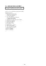
6-2. MECHANISM SECTION

ADJUSTMENTS

Refer to the separate “8 mm Video Mechanism Section Adjustment
Manual 

  B Mechanism  ” for adjustment, check procedure and

mechanical parts replacement.

2-1.

HOW TO OPERATE THE MECHANISM
AFTER THE CASSETTE COMPARTMENT IS
REMOVED

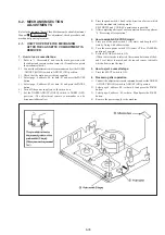
1. How to load a cassette tape:

1)

Refer to “1. Disassembly” and turn the main power on with
the cabinet and camera section removed.  (It enables to operate
the mechanical deck.)

2)

Connect the adjustment remote commander and set the NORM
-ADJUST (HOLD) switch to ADJUST (ON) position.

3)

Check that the main power is being supplied.

4)

Select page : 6, address: 00, set data : 01 and press the PAUSE
button.

5)

Select page : F, address: 02, set data : 01 and press the PAUSE
button.

6)

Turn off the power supply once, then turn it on.

7)

Set the NORM-ADJUST (HOLD) switch to NORM (OFF)
position. (The adjustment remote commander can be
disconnected hereafter.)

8)

Press the push-switch-1 knob in the direction of arrow which
sets the machine into loading mode.
PB, FF/REW and CUE/REV operations are possible.

9)

After completing all steps of above operation, be sure to perform
“4. Processing after operation”.

2. How to establish RECORD mode:

1)

Press pin of the push-switch 2 (ON state) and keep the ON
state by fixing with adhesive tape.

2)

Turn the main power switch ON (select VTR or CAMERA
position of camera).

3)

Set the RECORD switch to ON.
(When the test mode is selected, the rotation detection of the S
and T reel tables is muted, and the top end sensor is disable
which allow to run the tape.)

3. How to eject a cassette tape:

1)

Press the EJECT switch to ON.

4. Processing after operation

1)

Connect the adjustment remote commander and set the NORM
- ADJUST (HOLD) switch to ADJUST (ON) position.

2)

Select page 6, address : 00, set data : 01 and press the PAUSE
button.

3)

Select page: F, address : 02, set data : 00 and press the PAUSE
button.

4)

Remove the power supply to the machine.

Summary of Contents for Handycam CCD-TR501E

Page 1: ... TR506E TR720E TR740E PAL Australian Model CCD TR501E TR503E PAL Hong Kong Model CCD TR503E TR720E PAL Tourist Model CCD TR501E PAL SERVICE MANUAL VIDEO CAMERA RECORDER MICROFILM B MECHANISM SPECIFICATIONS For MECHANISM ADJUSTMENT refer to the 8mm Video MECHANICAL ADJUSTMENT MANUAL 9 973 801 11 Photo CCD TR506E Continued on next page CCD TR506PK is model that carring bag are added in CCD TR506 CCD...

Page 2: ...lithium battery cassette and shoulder strap 2 id 3 oz 1kg Including the battery pack NP 33 lithium battery CR2025 cassette P6 120 and shoulder strap Colour NTSC color EIR standards 15 Optical 30 Digital NTSC MODEL Monaural Phone jack When converted to 35mm still camera 39 585mm 1 9 16 23 1 8inches 0 4 lux at F1 4 0 4 to 100 000 lux 3 4W Table for difference of functions Model Video signal Viewfind...

Page 3: ...urface for solder splashes and bridges 2 Check the interboard wiring to ensure that no wires are pinched or contact high wattage resistors 3 Look for unauthorized replacement parts par ticularly transistors that were installed during a previous repair Point them out to the customer and recommend their replacement 4 Look for parts which through functioning show obvious signs of deterioration Point ...

Page 4: ...DIAGRAM 3 11 3 6 EVF BLOCK DIAGRAM 3 13 3 7 SERVO BLOCK DIAGRAM 3 15 3 8 POWER BLOCK DIAGRAM 3 18 4 PRINTED WIRING BOARDS AND SCHEMATIC DIAGRAMS 4 1 FRAME SCHEMATIC DIAGRAM 4 1 4 2 PRINTED WIRING BOARDS AND SCHEMATIC DIAGRAMS 4 4 VC 188 MAIN PRINTED WIRING BOARD 4 5 VC 188 CAMERA 1 SCHEMATIC DIAGRAM 4 13 VC 188 CAMERA 2 SCHEMATIC DIAGRAM 4 17 VC 188 VIDEO SCHEMATIC DIAGRAM 4 21 VC 188 MODE CONTROL...

Page 5: ...MENT 6 38 3 1 1 Equipment required 6 38 3 1 2 Precautions on adjustment 6 38 3 1 3 Adjustment connector VC 188 Board CN102 6 38 3 1 4 Equipment connection 6 39 3 1 5 Alignment tape 6 39 3 1 6 Output level and impedance 6 40 3 2 ADJUSTMENT POINTS WHEN MAJOR PARTS ARE REPLACED 6 41 1 When drum is replaced 6 41 3 3 POWER SUPPLY SYSTEM ADJUSTMENT 6 41 1 Power supply voltage check VC 188 board 6 41 2 V...

Page 6: ...power firstly remove the SCREW for TRIPOD then remove the FLEXIBLE BOARD as shown and finally connect the regulated power supply 5V to the loading motor this is to protect the main circuit from damage LOADING MOTOR FLEXIBLE BOARD From CN403 VC 188 SCREW forTRIPOD Regulated power supply 5V ...

Page 7: ......

Page 8: ......

Page 9: ......

Page 10: ......

Page 11: ......

Page 12: ......

Page 13: ......

Page 14: ......

Page 15: ......

Page 16: ......

Page 17: ......

Page 18: ......

Page 19: ......

Page 20: ......

Page 21: ......

Page 22: ......

Page 23: ......

Page 24: ......

Page 25: ...roove Insert S60 of the JK 153 board into groove Insert S60 of the JK 153 board into groove Insert S60 of the JK 153 board into groove Insert S60 of the JK 153 board into groove Insert S60 of the JK 153 board into groove Insert S60 of the JK 153 board into groove Insert S60 of the JK 153 board into groove 1 Screws 2 4 Screws B2 5 JK 153 BORAD groove 2 Screw 2 4 3 Screw 2 4 STEREO MODEL VIDEO LIGHT...

Page 26: ...ock the claws B 1 To remove the lids and board without having caught by claws the unit must be put in the EJECT mode See SERVICE NOTE on page 6 2 Unlock the claws A 4 Remove the cassette lid assembly in the direction of arrow Claw B Claw B Claw A Claw A 7 Screw M2 4 º Screws M2 3 8 JK 153 board AUDIO Mono 1P STEREO 2P SE 60 board Cassette compartment block Cassette compartment block 6 Flat cable 9...

Page 27: ... VC 188 BOARD 4 Screws M2 3 3 Screw M2 3 5 Screws B2 5 6 Lens frame 8 Screws B2 7 5 9 CD 163 board 1 Flexible board 2 Flat cable 7 Zoom lens ºIR 28 board IR MODEL VC 188 board VC 188 BOARD IR 28 4VC 188 board 2Cover 1 Screws M2 3 3 Flexible boards V C 1 8 8 B O A R D ...

Page 28: ...direction of the arrow while taking care of the claw 1 Flexible board 2 Flexible board CF 44 board Note When attaching the CF 44 board set the switches in the positions as shown claw claw claws S409 S410 S401 CF 44 BOARD CF 44 BOARD 3 Screw B2 5 7 EVF block assembly 5 Rotary flange 1 6 Flange slider 4 Screw B2 8 2 Screw B2 8 ...

Page 29: ...he direction of the arrow C D D C A claws C claw D claw C claw D claw D E E 6 Flexible board 8 LB 49 board Claw D is engaged with D 7 VF 109 board Claw C is engaged with C 9 Prism holder assembly Claw E is engaged with E º LCX005BK 5 Remove the flexible board from the VF 110 board LCD cushion claws B claws E VF LENS assembly Flexible board VF 110 board Claw B is engaged with B 1 Screw M2 4 2 Screw...

Page 30: ...2 6 2 11 INTERNAL VIEWS LEFT SIDE RIGHT SIDE ...

Page 31: ... DD 94 POWER JK 153 JACK MA 295 AUDIO VC 188 MAIN IR 28 INFRARED COMMUNICATION CF 44 SYSTEM CONTROL CD 163 CCD IMAGER VF 109 H AFC VF 110 RGB DECODER LB 49 BACK LIGHT FP 249 MODE SENSOR SE 60 STEADY SHOT STEADY SHOT MODEL DD 94 POWER JK 153 JACK MA 295 AUDIO VC 188 MAIN CF 44 SYSTEM CONTROL VF 102 EVF CD 163 CCD IMAGER ...

Page 32: ......

Page 33: ......

Page 34: ......

Page 35: ......

Page 36: ......

Page 37: ......

Page 38: ......

Page 39: ......

Page 40: ......

Page 41: ......

Page 42: ......

Page 43: ......

Page 44: ......

Page 45: ......

Page 46: ......

Page 47: ......

Page 48: ......

Page 49: ......

Page 50: ......

Page 51: ......

Page 52: ......

Page 53: ......

Page 54: ......

Page 55: ......

Page 56: ......

Page 57: ......

Page 58: ......

Page 59: ......

Page 60: ......

Page 61: ......

Page 62: ...our la sécurité Ne les remplacer que par une pièce portant le numéro spécifie CCD TR86 TR96 TR506 TR506PK TR507 TR916 NTSC CCD TR501E TR502E TR503E TR506E TR620E TR720E TR740E PAL 5 1 1 OVERALL SECTION Ref No Part No Description Remarks Ref No Part No Description Remarks 1 3 962 826 01 SCREW 2X4 2 3 713 786 21 SCREW M2X3 3 X 3945 446 4 LID ASSY CASSETTE TR916 TR501E 3 X 3947 229 1 LID ASSY G CASSE...

Page 63: ...3946 890 1 PANEL ASSY FRONT TR501E 64 X 3947 261 1 PANEL ASSY VL FRONT TR86 TR96 64 X 3947 317 1 PANEL ASSY G FRONT TR502E TR503E TR620E 64 X 3947 344 1 PANEL ASSY LC FRONT TR506 TR506E TR720E 64 X 3947 347 1 PANEL ASSY SVL FRONT TR507 TR740E 64 X 3947 405 1 PANEL ASSY BG FRONT TR916 65 3 974 899 01 KNOB POWER 66 3 719 601 01 SCREW B2X5 TAPPING 67 3 961 823 01 SPRING L COVER 68 3 965 034 01 SPRING...

Page 64: ... TR503E TR506E TR620E TR720E 115 3 965 879 01 SLIDER BT 116 3 974 205 01 KNOB 2P TR96 TR916 TR620E TR720E TR740 117 3 974 204 01 KNOB 3P 118 3 974 202 01 BUTTON 1 CF TR501E TR503E 118 3 974 202 11 BUTTON 1 CF EXCEPT TR501E TR503E 119 3 974 203 01 BUTTON 2 CF TR506 TR501E TR502E TR503E TR506E 119 3 974 203 11 BUTTON 2 CF TR86 TR96 TR507 TR916 TR620E TR720E TR740E 120 3 944 328 01 COVER LIQUID CRYST...

Page 65: ...156 1 782 155 11 CABLE FLEXIBLE FLAT 16P 157 A 7073 091 A IR 28 BOARD COMPLETE TR86 TR96 TR507 TR916 157 A 7073 142 A IR 28 BOARD COMPLETE TR740E 158 1 665 151 11 FP 550 FLEXIBLE BOARD 159 3 975 367 01 FRAME MD 160 1 665 150 11 FP 549 FLEXIBLE BOARD TR86 TR96 TR916 TR620E TR720E TR740E 161 A 7073 087 A SE 60 BOARD COMPLETE TR96 TR916 161 A 7073 129 A SE 60 BOARD COMPLETE TR86 161 A 7073 145 A SE 6...

Page 66: ...LETE TR86 TR96 TR506 TR507 TR916 204 A 7073 089 A VF 110 BOARD COMPLETE TR503E TR506E TR720E TR740E 205 X 3946 887 1 VF LENS ASSY 207 3 960 302 11 CUSHION 1 LCD 208 8 756 016 10 LCX005BK 5 209 X 3946 886 1 HOLDER ASSY PRISM 210 A 7073 086 A LB 49 BOARD COMPLETE TR86 TR96 TR506 TR507 TR916 210 A 7073 090 A LB 49 BOARD COMPLETE TR503E TR506E TR720E TR740E 211 A 7073 084 A VF 109 BOARD COMPLETE TR86 ...

Page 67: ...NET R EVF TR502E TR620E 256 3 974 155 11 CABINET R EVF TR501E 257 X 3947 303 1 COVER ASSY CRT 258 1 782 156 11 CABLE FLEXIBLE FLAT 5P 259 1 452 673 31 CRT ASSY M01KXX90WB TR501E TR502E TR620E 260 A 7073 078 A VF 102 BOARD COMPLETE Note The components identified by mark or dotted line with mark are critical for safety Replace only with part number specified Note Les composants identifiés par une ma...

Page 68: ... Remarks Ref No Part No Description Remarks 501 8 848 710 01 LENS ZOOM LSV 510A 502 A 4910 808 A LSV 510A LENS DEVICE 503 3 713 791 41 SCREW M1 7X5 TAPPING P2 504 3 708 302 01 SCREW BT3 P1 7X4C M905 1 698 760 01 STEPPING MOTOR FOCUS M906 1 698 759 01 STEPPING MOTOR ZOOM ...

Page 69: ...R ASSY 702 7 624 102 04 STOP RING 1 5 TYPE E 703 X 3945 400 1 CASSETTE COMPARTMENT ASSY 704 3 965 587 03 SPRING TENSION 705 3 965 584 01 RETAINER GOOSENECK 706 3 973 268 01 SPRING TENSION 707 X 3945 399 1 GEAR ASSY GOOSENECK 708 3 947 503 01 SCREW M1 4X2 5 709 3 727 176 01 WASHER 710 3 971 076 01 FASTENER D 711 3 976 055 01 SCREW M1 4X1 ...

Page 70: ...65 568 01 GUIDE LOCK 769 3 965 562 01 SPRING RATCHET TENSION 770 3 965 581 01 RATCHET T 771 X 3945 394 1 ARM ASSY PINCH 772 X 3945 398 1 DECK ASSY REEL T 773 3 965 648 01 SPRING PINCH TENSION 774 3 965 579 01 ROLLER PINCH PRESS 775 3 965 563 01 GEAR T SOFT 776 3 965 565 01 CLAW T SOFT 777 X 3945 397 1 DECK ASSY REEL S 778 X 3945 396 1 BAND ASSY TENSION REGULATOR 779 3 945 756 01 SCREW M1 4X3 780 3...

Page 71: ...01 PLATE REGULATOR TENSION 819 3 965 536 01 SPRING TENSION 820 X 3945 388 1 SLIDER ASSY GL 821 3 965 532 01 ARM LS 822 3 965 535 01 SPRING TENSION 823 3 965 542 01 SHIELD MOTOR 824 3 965 539 01 GEAR A 825 3 965 538 01 SLEEVE MOTOR HOLDER 826 3 965 540 01 HOLDER MOTOR 827 3 965 541 01 SHAFT WORM 828 3 321 393 01 WASHER STOPPER 829 3 965 724 01 SPRING TORSION 830 A 7040 423 A ROLLER BLOCK ASSY HC 83...

Page 72: ...CK ASSY ICX207AK 43 TR502E TR506E IC790 A 7030 794 A CCD BLOCK ASSY MN37113FP TR86 COIL L401 1 414 757 11 INDUCTOR 100uH TRANSISTOR Q401 8 729 232 86 TRANSISTOR 2SK1875 TE85L Q402 8 729 117 73 TRANSISTOR 2SC4178 F13F14 T1 RESISTOR R403 1 216 833 11 METAL CHIP 10K 5 1 16W R404 1 216 829 11 METAL CHIP 4 7K 5 1 16W R407 1 216 295 91 CONDUCTOR CHIP 2012 A 7093 254 A CF 44 BOARD COMPLETE TR501E A 7093 ...

Page 73: ... 015 76 TRANSISTOR UN5211 TX Q409 8 729 823 16 TRANSISTOR 2SC4555 5 6 7 TL Q410 8 729 420 24 TRANSISTOR 2SB1218A QRS TX R86 TR96 TR916 Q411 8 729 023 89 TRANSISTOR 2SJ305 TE85L Q412 8 729 015 76 TRANSISTOR UN5211 TX Q413 8 729 230 63 TRANSISTOR 2SD1819A QRS TX R86 TR96 TR916 RESISTOR R401 1 216 864 11 METAL CHIP 0 5 1 16W R402 1 216 864 11 METAL CHIP 0 5 1 16W R408 1 216 853 11 METAL CHIP 470K 5 1...

Page 74: ...P 1 5K 5 1 16W R502 1 216 831 11 METAL CHIP 6 8K 5 1 16W R503 1 216 845 11 METAL CHIP 100K 5 1 16W R504 1 216 845 11 METAL CHIP 100K 5 1 16W R505 1 216 809 11 METAL CHIP 100 5 1 16W R506 1 216 826 11 METAL CHIP 2 7K 5 1 16W R507 1 216 817 11 METAL CHIP 470 5 1 16W TR96 TR916 R507 1 216 864 11 METAL CHIP 0 5 1 16W EXCEPT TR96 TR916 R508 1 216 817 11 METAL CHIP 470 5 1 16W TR96 TR916 R508 1 216 864 ...

Page 75: ... 1uF 10 16V C044 1 164 346 11 CERAMIC CHIP 1uF 16V C045 1 126 395 11 ELECT 22uF 20 16V C046 1 128 006 11 ELECT CHIP 4 7uF 20 25V C049 1 164 489 11 CERAMIC CHIP 0 22uF 10 16V TR86 TR96 TR916 CONNECTOR CN003 1 691 935 11 CONNECTOR BOARD TO BOARD 38P CN005 1 770 620 21 PIN CONNECTOR 3P TR86 TR96 TR916 DIODE D001 8 719 989 33 DIODE FC806 TL D002 8 719 420 14 DIODE MA8082 TX FUSE F001 1 533 483 11 FUSE...

Page 76: ...Ref No 5 000 Series 1 658 214 11 FP 356 FLEXIBLE PRINT BOARD 3 965 551 01 HOLDER S SENSOR 3 965 552 01 HOLDER T SENSOR HOLE ELEMENT H001 8 719 033 37 ELEMENT HALL HW 105C H002 8 719 033 37 ELEMENT HALL HW 105C TRANSISTOR Q001 8 729 907 25 PHOTO TRANSISTOR PT4850F Q002 8 729 907 25 PHOTO TRANSISTOR PT4850F SWITCH S001 1 692 614 11 SWITCH PUSH 3 KEY REC PROOF S002 1 572 688 11 SWITCH PUSH 1 KEY C C ...

Page 77: ...IP 4 7K 5 1 16W R035 1 216 829 11 METAL CHIP 4 7K 5 1 16W R036 1 216 823 11 METAL CHIP 1 5K 5 1 16W R039 1 216 832 11 METAL CHIP 8 2K 5 1 16W R041 1 216 833 11 METAL CHIP 10K 5 1 16W R043 1 216 847 11 METAL CHIP 150K 5 1 16W R044 1 216 847 11 METAL CHIP 150K 5 1 16W R046 1 216 864 11 METAL CHIP 0 5 1 16W A 7073 076 A JK 153 BOARD COMPLETE TR501E AEP TR502E TR620E A 7073 071 A JK 153 BOARD COMPLETE...

Page 78: ... 11 CERAMIC CHIP 0 047uF 10 16V TR506 TR507 TR506E TR720E TR740E C959 1 107 826 11 CERAMIC CHIP 0 1uF 10 16V TR506 TR507 TR506E TR720E TR740E C960 1 109 982 11 CERAMIC CHIP 1uF 10 10V TR506 TR507 TR506E TR720E TR740E C961 1 107 826 11 CERAMIC CHIP 0 1uF 10 16V TR506 TR507 TR506E TR720E TR740E C962 1 107 826 11 CERAMIC CHIP 0 1uF 10 16V TR506 TR507 TR506E TR720E TR740E C963 1 162 927 11 CERAMIC CHI...

Page 79: ... INDUCTOR FERRITE BEAD TR506 TR507 TR506E TR720E TR740E R954 1 216 824 11 METAL CHIP 1 8K 5 1 16W TR506 TR507 TR506E TR720E TR740E R955 1 414 228 11 INDUCTOR FERRITE BEAD R956 1 414 228 11 INDUCTOR FERRITE BEAD R957 1 216 829 11 METAL CHIP 4 7K 5 1 16W TR506 TR507 TR506E TR720E TR740E R958 1 216 838 11 METAL CHIP 27K 5 1 16W TR506 TR507 TR506E TR720E TR740E R959 1 216 831 11 METAL CHIP 6 8K 5 1 16...

Page 80: ...664 1 162 927 11 CERAMIC CHIP 100PF 5 50V TR96 TR916 TR620E TR720E TR740E C665 1 110 501 11 CERAMIC CHIP 0 33uF 10 16V TR96 TR916 TR620E TR720E TR740E C666 1 110 501 11 CERAMIC CHIP 0 33uF 10 16V TR96 TR916 TR620E TR720E TR740E C667 1 162 970 11 CERAMIC CHIP 0 01uF 10 25V TR96 TR916 TR620E TR720E TR740E C668 1 135 259 11 TANTAL CHIP 10uF 20 6 3V TR96 TR916 TR620E TR720E TR740E CONNECTOR CN650 1 76...

Page 81: ...24 1 164 227 11 CERAMIC CHIP 0 022uF 10 25V C125 1 162 970 11 CERAMIC CHIP 0 01uF 10 25V TR86 TR96 TR506 TR507 TR916 C126 1 162 970 11 CERAMIC CHIP 0 01uF 10 25V TR86 TR96 TR506 TR507 TR916 C127 1 162 970 11 CERAMIC CHIP 0 01uF 10 25V C128 1 135 259 11 TANTAL CHIP 10uF 20 6 3V C129 1 162 970 11 CERAMIC CHIP 0 01uF 10 25V TR86 TR96 TR506 TR507 TR916 C130 1 162 970 11 CERAMIC CHIP 0 01uF 10 25V C131...

Page 82: ...68PF 5 50V TR86 TR96 TR506 TR507 TR916 C244 1 162 970 11 CERAMIC CHIP 0 01uF 10 25V TR501E TR502E TR503E TR506E TR620E TR720E TR740E C244 1 164 315 11 CERAMIC CHIP 470PF 5 50V TR86 TR96 TR506 TR507 TR916 C245 1 162 912 11 CERAMIC CHIP 7PF 0 5PF 50V TR501E TR502E TR503E TR506E TR620E TR720E TR740E C245 1 162 917 11 CERAMIC CHIP 15PF 5 50V TR86 TR96 TR506 TR507 TR916 C246 1 135 073 00 TANTALUM CHIP ...

Page 83: ...512 1 162 968 11 CERAMIC CHIP 0 0047uF 10 50V TR506 TR507 TR506E TR720E TR740E C513 1 115 467 11 CERAMIC CHIP 0 22uF 10 10V TR86 TR96 TR916 TR501E TR502E TR503E TR620E C514 1 162 925 11 CERAMIC CHIP 68PF 5 50V C515 1 162 960 11 CERAMIC CHIP 220PF 10 50V TR501E TR502E TR503E TR620E C515 1 162 957 11 CERAMIC CHIP 220PF 5 50V TR86 TR96 TR916 C516 1 135 149 21 TANTALUM CHIP 2 2uF 20 10V TR506 TR507 TR...

Page 84: ... 1 164 156 11 CERAMIC CHIP 0 1uF 25V C717 1 162 964 11 CERAMIC CHIP 0 001uF 10 50V C718 1 162 913 11 CERAMIC CHIP 8PF 0 5PF 50V C719 1 164 489 11 CERAMIC CHIP 0 22uF 10 16V C722 1 162 964 11 CERAMIC CHIP 0 001uF 10 50V C725 1 162 970 11 CERAMIC CHIP 0 01uF 10 25V C726 1 135 259 11 TANTAL CHIP 10uF 20 6 3V C727 1 135 091 00 TANTALUM CHIP 1uF 20 16V C728 1 135 091 00 TANTALUM CHIP 1uF 20 16V C729 1 ...

Page 85: ...FB708 1 414 228 11 INDUCTOR FERRITE BEAD IC IC101 8 752 071 15 IC CXA1702AR T6 IC201 8 752 075 45 IC CXA2051R T6 IC202 8 759 035 90 IC TC7S02F TE85R IC205 8 759 295 66 IC BA7653AF E2 IC206 8 759 295 66 IC BA7653AF E2 IC302 8 759 290 12 IC M62370GP 650D IC303 8 759 449 47 IC uPD6466GS 610 GLG E2 IC304 8 759 391 88 IC MC14066BDTR2 IC400 8 752 880 05 IC CXP87460 011R IC401 8 759 445 93 IC AK6440AM E2...

Page 86: ...ANSISTOR 2SD1819A QRS TX Q202 8 729 230 63 TRANSISTOR 2SD1819A QRS TX Q206 8 729 420 24 TRANSISTOR 2SB1218A QRS TX Q208 8 729 402 42 TRANSISTOR UN5213 TX Q211 8 729 420 24 TRANSISTOR 2SB1218A QRS TX TR86 TR96 TR506 TR507 TR916 Q213 8 729 402 42 TRANSISTOR UN5213 TX Q214 8 729 420 24 TRANSISTOR 2SB1218A QRS TX Q215 8 729 013 15 TRANSISTOR 2SC4909 TL Q216 8 729 420 20 TRANSISTOR XN4312 TW TR501E TR5...

Page 87: ...HIP 560 5 1 16W R157 1 216 822 11 METAL CHIP 1 2K 5 1 16W R158 1 216 809 11 METAL CHIP 100 5 1 16W R159 1 216 818 11 METAL CHIP 560 5 1 16W R160 1 216 818 11 METAL CHIP 560 5 1 16W R163 1 216 813 11 METAL CHIP 220 5 1 16W R164 1 216 818 11 METAL CHIP 560 5 1 16W R165 1 216 829 11 METAL CHIP 4 7K 5 1 16W R167 1 216 818 11 METAL CHIP 560 5 1 16W R168 1 216 818 11 METAL CHIP 560 5 1 16W R169 1 216 81...

Page 88: ...E TR502E TR503E TR506E TR620E TR720E TR740E R263 1 216 829 11 METAL CHIP 4 7K 5 1 16W TR86 TR96 TR506 TR507 TR916 R265 1 216 821 11 METAL CHIP 1K 5 1 16W TR501E TR502E TR503E TR506E R266 1 216 864 11 METAL CHIP 0 5 1 16W R267 1 216 864 11 METAL CHIP 0 5 1 16W R268 1 216 818 11 METAL CHIP 560 5 1 16W TR501E TR502E TR503E TR506E R270 1 216 818 11 METAL CHIP 560 5 1 16W TR501E TR502E TR503E TR506E TR...

Page 89: ... TR96 TR916 R421 1 216 821 11 METAL CHIP 1K 5 1 16W R422 1 216 845 11 METAL CHIP 100K 5 1 16W R423 1 216 845 11 METAL CHIP 100K 5 1 16W TR86 TR96 TR916 R424 1 216 843 11 METAL CHIP 68K 5 1 16W TR740E R424 1 216 841 11 METAL CHIP 47K 5 1 16W TR502E TR720E R424 1 216 837 11 METAL CHIP 22K 5 1 16W TR501E TR503E TR620E R424 1 216 845 11 METAL CHIP 100K 5 1 16W TR86 TR506 TR506E R425 1 216 833 11 METAL...

Page 90: ... 5 1 16W TR506 TR507 TR506E TR720E TR740E R534 1 216 864 11 METAL CHIP 0 5 1 16W TR86 TR96 TR916 TR501E TR502E TR503E TR620E R537 1 216 829 11 METAL CHIP 4 7K 5 1 16W TR506 TR507 TR506E TR720E TR740E R537 1 216 864 11 METAL CHIP 0 5 1 16W TR86 TR96 TR916 TR501E TR502E TR503E TR620E R556 1 216 853 11 METAL CHIP 470K 5 1 16W R562 1 216 864 11 METAL CHIP 0 5 1 16W R564 1 216 864 11 METAL CHIP 0 5 1 1...

Page 91: ...18 891 11 METAL GLAZE 68K 0 50 1 16W TR96 TR916 TR620E TR720E TR740E R781 1 216 864 11 METAL CHIP 0 5 1 16W TR86 TR506 TR507 TR502E TR506E R782 1 216 821 11 METAL CHIP 1K 5 1 16W EXCEPT TR502E R783 1 216 845 11 METAL CHIP 100K 5 1 16W EXCEPT TR502E R784 1 216 821 11 METAL CHIP 1K 5 1 16W EXCEPT TR502E SWITCH S301 1 771 029 21 SWITCH TACTILE PAUSE S302 1 771 029 21 SWITCH TACTILE STOP S303 1 771 02...

Page 92: ... ASSY CRT A 7073 088 A VF 109 BOARD COMPLETE TR503E TR506E TR720E TR740E A 7073 084 A VF 109 BOARD COMPLETE TR86 TR96 TR506 TR507 TR916 Ref No 7 000 Series CAPACITOR C851 1 162 974 11 CERAMIC CHIP 0 01uF 50V C852 1 162 974 11 CERAMIC CHIP 0 01uF 50V C853 1 104 916 11 TANTAL CHIP 6 8uF 20 20V C854 1 164 227 11 CERAMIC CHIP 0 022uF 10 25V C855 1 162 974 11 CERAMIC CHIP 0 01uF 50V C856 1 135 259 11 T...

Page 93: ... C723 1 162 974 11 CERAMIC CHIP 0 01uF 50V C724 1 164 227 11 CERAMIC CHIP 0 022uF 10 25V C725 1 162 974 11 CERAMIC CHIP 0 01uF 50V C726 1 164 156 11 CERAMIC CHIP 0 1uF 25V TR503E TR506E TR720E TR740E C729 1 163 077 00 CERAMIC CHIP 0 1uF 10 25V TR86 TR96 TR506 TR507 TR916 C729 1 104 912 11 TANTAL CHIP 3 3uF 20 16V TR503E TR506E TR720E TR740E C728 1 162 974 11 CERAMIC CHIP 0 01uF 50V C730 1 163 077 ...

Page 94: ...49 1 216 833 11 METAL CHIP 10K 5 1 16W R750 1 216 841 11 METAL CHIP 47K 5 1 16W R753 1 216 839 11 METAL CHIP 33K 5 1 16W R754 1 216 839 11 METAL CHIP 33K 5 1 16W R755 1 216 839 11 METAL CHIP 33K 5 1 16W R756 1 216 833 11 METAL CHIP 10K 5 1 16W R757 1 216 839 11 METAL CHIP 33K 5 1 16W R761 1 216 821 11 METAL CHIP 1K 5 1 16W R762 1 216 838 11 METAL CHIP 27K 5 1 16W R763 1 216 842 11 METAL CHIP 56K 5...

Page 95: ...HINESE TR506 TR507 3 859 173 11 MANUAL INSTRUCTION ENGLISH RUSSIAN TR501E E Australiaan Tourist TR503E TR506E TR720E TR740E 3 859 173 21 MANUAL INSTRUCTION FRENCH GERMAN TR501E E Tourist TR503E E HongKong TR506E TR720E TR740E 3 859 173 31 MANUAL INSTRUCTION ARABIC PORUTUGUESE TR501E E TR503E E TR506E TR720E E TR740E 3 859 173 41 MANUAL INSTRUCTION CHINESE TR501E E TR503E E TR506E TR720E E TR740E 3...

Page 96: ... MODEL WIDE WIDE 16 9 MODEL DZ DIGITAL ZOOM TYPE MO MONO MODEL ST STEREO MODEL V LIGHT VIDEO LIGHT TYPE IR INFRARED RADIATION TYPE S SHOT STEADY SHOT MODEL Ref No J 1 J 2 J 3 J 4 J 5 J 6 J 7 J 8 J 9 Name Filter for color temperature correction C14 ND filter 1 0 ND filter 0 3 Pattern box PTB 450 Color chart for pattern box Siemens star Adjustment remote commander RM 95 upgraded Note Multi CPC Measu...

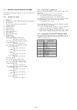
Page 97: ...olor picture on the monitor TV shown in Fig 6 1 3 b have been acquired Maintain this setup until adjustment is complete Fig 6 1 3 4 Chart for flange back adjustment Join together a piece of white A0 size paper 1189mm 841 mm and a piece of black paper to make the chart shown in Fig 6 1 4 Note Use a non reflecting and non glazing vellum paper The size must be A0 or larger and the joint between the w...

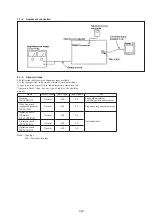
Page 98: ...sassembly for details of how to remove the cabinet and the respective boards Note 2 Removal of the lens block and VC 188 board is not necessary if only adjustments are to be made 1 Connect the adjustment equipment as shown in Fig 6 1 5 Fig 6 1 5 ...

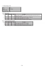
Page 99: ...emote commander to the ADJ or ON service position If the adjustment remote commander is correctly connected the adjustment remote commander s LED will show the display as shown in Fig 6 1 6 3 Bit value discrimination It is necessary to discriminate between the bit values with the data displayed on the adjustment remote commander for all following items Identify whether the bit value is 1 or 0 with...

Page 100: ...he address The address increases when the FF button is pressed and decreases when the REW 0 button is pressed Altogether there are 256 addresses from address 00 to address FF Some addresses which are not used during adjustment do not appear Taking note the already stored adjustment data The previous adjustment can be erased if the adjustment remote commander is incorrectly handled To prevent this ...

Page 101: ...0 11 12 13 14 15 16 17 18 19 1A 1B 1C 1D 1E 1F 20 21 22 23 24 25 26 27 28 29 2A 2B Initial Value 00 00 00 00 00 00 00 00 00 00 00 00 00 00 00 00 00 00 00 48 03 00 00 0C 00 0C 80 Memo Column Adjustment Data Address 2C 2D 2E 2F 30 31 32 33 34 35 36 37 38 39 3A 3B 3C 3D 3E 3F 40 41 42 43 44 45 46 47 48 49 4A 4B 4C 4D 4E 4F 50 51 52 53 54 55 56 57 Initial Value 40 40 80 9E PAL B9 NT 68 PAL 53 NT 7E PA...

Page 102: ...760 A2 NT 760 41 PAL 510 46 NT 510 20 PAL 760 20 NT 760 Memo Column Adjustment Data Address 7F 80 81 82 83 84 85 86 87 88 89 8A 8B 8C 8D 8E 8F 90 91 92 93 94 95 96 97 98 99 9A 9B 9C 9D 9E 9F A0 A1 A2 A3 A4 CB CC E3 E4 EF F0 FF Initial Value 83 67 5C 4A 5C 33 A0 V LIGHT NT A2 V LIGHT PAL 28 PAL 510 30 NT 510 28 PAL 760 30 NT 760 1A PAL 510 20 NT 510 1A PAL 760 20 NT 760 6A 58 33 04 A2 88 65 44 55 0...

Page 103: ...PAUSE button 3 F 02 21 After setting the data press the PAUSE button 4 Turn off the UNREG power supply once then turn it on 5 6 00 00 After setting the data press the PAUSE button 2 Power supply voltage check VC 188 board Subject Any subject Measuring equipment Digital voltmeter DIG3V check Measurement Point CN301 Pin CN301 Pin MT GND Specification Value 3 15 0 1Vdc MT5V check Measurement Point CN...

Page 104: ...urn OFF and ON the main power supply Preparation 2 6 00 01 After setting the data 01 to the address press the PAUSE button 3 6 11 Confirm that the data is 00 4 6 01 2D After setting the data Press the PAUSE button Execution of page F data initialization By this operation all the data from address 01 to EF are initialized 5 6 11 Confirm that the data is 01 Order Page Address Data Procedure 1 6 01 0...

Page 105: ...9 77 77 76 76 77 20 20 A0 A0 6E 6E 8D 8F 98 80 4A 1B 40 48 25 B6 A3 B2 46 09 66 TR96 E1 96 07 04 1C 42 36 26 BA C3 B1 20 00 TR506 03 D5 0C 05 06 01 80 06 64 FF F4 77 20 45 48 B6 A3 B2 46 09 TR507 2C 07 01 4A 25 TR916 02 E1 09 16 00 30 07 04 FE FC 99 1C 42 36 26 BA C3 B1 20 00 AEP 04 91 54 04 04 05 01 15 00 74 D8 D8 C6 C1 FF F1 AA 8C 55 7B 78 92 91 80 3C 1B 8A 80 80 90 4C 21 46 48 B1 B3 81 41 09 Da...

Page 106: ...66 66 66 59 5D 3A 20 F0 04 DA CF 04 A8 TR507 04 TR916 01 6B 62 6C 57 64 3C A0 D0 0F 8A D1 03 B8 AEP 05 66 66 66 59 5D 3A 22 F0 28 1A 04 CE 02 A8 Data E AUS HK CE 04 E 05 66 9F 62 66 57 64 20 3A 22 1B F0 28 1A 64 04 DA D0 02 A8 5E AEP 8A TR503E 66 59 5D CE 04 TR506E 64 DA D0 AEP 03 6B 6C 5C 5D 3C 8A D2 02 B8 UK DA TR502E TR620E TR501E TR720E 04 TR740E Same data as that of the left column ...

Page 107: ...numbers on the DDS display or on the adjustment remote commander Maintenance engineers are expected to convert the displayed hexadecimal numbers to the corresponding decimal numbers using Order Page Address Data Procedure 1 6 00 01 After setting the data press the PAUSE button Preparation 2 F 3D Change the data using PLAY STOP buttons until the frequency satisfies the specification 3 F 3D Press th...

Page 108: ...decimal number is 2100 1 2100 256 8 203125 A 2 B 3 8 203125 8 256 16 3 25 C 4 D 5 3 25 3 16 4 E 6 2100 834 h is obtained If the decimal number fall into the category 3 1 Divide the decimal number by 4096 Result is A 2 Take the integer portion of the number A as B 3 Calculate the equation A B 4096 256 Result is C 4 Take the integer portion of the number C as D 5 Calculate the equation C D 256 16 Re...

Page 109: ...pearing on the DDS display note The read out data is W1 9 6 01 01 After setting the data press the PAUSE button 10 F 40 30 After setting the data press the PAUSE button Read the data appearing on the DDS display note The read out data is K1 11 F 40 40 After setting the data press the PAUSE button Read the data appearing on the DDS display note The read out data is K2 12 Convert the data W1 W2 K1 a...

Page 110: ... over as a unit and cut away the rest 24 F 40 Set the data X2 which is the result of calculation in step 23 25 Press the PAUSE button 26 F 41 Change data using PLAY and STOP button until 7Bh appears on the DDS display 27 Press the PAUSE button 28 6 01 01 After setting the data press the PAUSE button 29 Confirm that the DDS display shows the data in the range from 13 to 17 Order Page Address Data P...

Page 111: ...us Order Page Address Data Procedure 1 Check that the center of the flange back adjustment chart coincides with that of the display on the monitor at both ends TELE end and the WIDE end of the zoom lens 2 6 00 01 After setting the data press the PAUSE button Preparation 3 Confirm that the data at page F address 52 to 59 is the initial value referring to the Page F address list 4 6 11 Confirm that ...

Page 112: ...out of focus 1 Picture is in focus Order Page Address Data Procedure 1 Place a Siemens star at 2 meters in front of lens 2 Decrease illumination to the chart down to a point before noise appears on monitor TV in order to fully open the IRIS 3 6 42 02 After setting the data press the PAUSE button 4 6 43 01 After setting the data press the PAUSE button 5 Shoot the Siemens star at TELE end 6 Confirm ...

Page 113: ...01E TR503E MODEL Setting procedure Order Procedure 1 Turn OFF the auto focus 2 Adjust the focus using the focus knob 3 Adjust direction and zoom of camera so that the picture frame is adjusted as specified by Fig 6 1 8 and Fig 6 1 9 4 Write down markings on the picture frame on the monitor screen If the color bar chart standard picture frame or white pattern standard picture frame is specified in ...

Page 114: ... Page Address Data Procedure Condition 1 6 00 01 After setting the data press the PAUSE button Preparation 2 6 42 02 After setting the data press the PAUSE button 3 6 03 00 After setting the data press the PAUSE button Setting 4 F 80 Take note of the data 5 F 80 00 After setting the data press the PAUSE button 6 6 01 37 After setting the data press the PAUSE button 43 44 Change the data so that re...

Page 115: ...s Data Procedure 1 6 00 01 After setting the data press the PAUSE button Preparation 2 F 02 21 After setting the data press the PAUSE button 3 Turn off the UNREG power supply once then turn it on 4 6 00 01 After setting the data press the PAUSE button 5 6 11 Confirm that the date is 00 6 6 01 4B After setting the data press the PAUSE button 7 6 01 49 After setting the data press the PAUSE button 8...

Page 116: ...djustment Order Page Address Data Procedure 1 Turn the main power OFF then to ON 2 Shoot a white pattern with the standard picture frame 3 6 00 01 After setting the data press the PAUSE button 4 6 11 Confirm that data is 00 5 6 01 11 After setting the data press the PAUSE button 6 6 01 0D After setting the data press the PAUSE button Executes the auto white balance reference data input 7 6 11 If d...

Page 117: ...g after Adjustments Order Page Address Data Procedure 1 6 00 01 After setting the data press the PAUSE button Preparation 2 6 02 01 After setting the data press the PAUSE button 3 6 42 02 Steady shot model only After setting the data press the PAUSE button 4 6 04 58 After setting the data press the PAUSE button 5 6 01 19 After setting the data press the PAUSE button 6 F 42 08 After setting the dat...

Page 118: ...XX 3 F F6 Read the data of this address The read out data should be used as the specification value calculation data YY 4 6 00 01 After setting the data press the PAUSE button Preparation 1 5 F 02 21 After setting the data press the PAUSE button Preparation 2 6 Turn off the UNREG power supply once then turn it on 7 6 00 01 After setting the data press the PAUSE button 8 6 01 35 After setting the d...

Page 119: ...ck that the lens is not covered by either filter 2 6 01 0F After setting the data press the PAUSE button 3 Check that the white luminance point is located within the circle Without filter shown in Fig 6 1 10 a 4 6 01 00 After setting the data press the PAUSE button 5 6 01 23 After setting the data press the PAUSE button 6 Put the C14 filter on the lens 7 Check that the white luminance point is loc...

Page 120: ...tion 2 Adjust SE651 vertical direction correction first Read the sensor sensitivity value which is indicated on the replacement gyro sensor SE651 Calculate the following equation decimal calculation to obtain the D1 Note 3 D1 95 NTSC SE651 sensor sensitivity value D1 114 PAL SE651 sensor sensitivity value 3 F 5A Round the number D1 to count fractions of 0 5 and over as a unit and cut away the rest...

Page 121: ...901 Pin 1 Specification Value 4 65 0 1Vdc 18 2 Horizontal and vertical position Purpose Maintains horizontal position Adjustment error Horizontal position cannot be maintained Signal Monoscope signal Adjustment RV905 Specification Value Overscan 3 5 3 5 horizontal one side Overscan 4 5 1 5 vertical one side Adjustment procedure Order Procedure 1 Confirm that the horizontal and vertical picture siz...

Page 122: ...lution is 300 lines or more Adjustment procedure Order Procedure 1 Adjust focus ring for optimum focus Confirm that the horizontal resolution satisfies the specification 18 6 Diffraction adjustment Signal Dot pattern Monoscope signal Adjustment DY diffraction adjustment ring Specification Value Refer to the illustration below Adjustment procedure Order Procedure 1 Adjust the diffraction adjustment...

Page 123: ...ect Measuring Equipment Digital voltmeter EVF 5V check Measuring Point CN851 pin 5 Specification Value 4 65 0 05Vdc EVF15 V check Measuring Point CN851 pin 7 Specification Value 15 0 0 05Vdc Pin No 1 2 3 4 5 6 7 8 9 10 Signal Name LC COM EVF GND G OUT 13 5V N C 12V R OUT B OUT SLYT PCO VF 110 BOARD SIDE A VF 109 BOARD SIDE A Fig 6 1 13 Preparation Because this machine does not have VIDEO INPUT con...

Page 124: ...justment Page F Adjustment Address D2 Specification Value A 1 80 0 05V Adjustment procedure Order Page Address Data Procedure 1 6 00 01 Set the data 2 CC A0 CD AE 75 CE 95 50 CF 7A D0 6A D1 70 F D2 90 After setting the data press the PAUSE button D3 40 D4 7A D5 7A D6 70 D7 05 3 6 00 00 Set the data Order Page Address Data Procedure 1 6 00 01 Set the data Preparation 2 Check the GND level on an osc...

Page 125: ...or close to saturated image Mode Playback Signal Signal Measurement Point CN702 pin 3 G OUT on VF 110 board Measuring Equipment Oscilloscope Adjustment Page F Adjustment Address D1 Specification A 2 0 0 1Vp p NTSC A 2 0 0 1Vp p PAL Connection 1 Connect CN702 pin 3 and pin 2 EVF GND using a 3300 resistor 1 249 423 11 Adjustment Procedure Order Page Address Data Procedure 1 6 00 01 Set the data Prep...

Page 126: ...alance on the EVF Measuring Equipment screen Adjustment Page F Adjustment Address CF D0 Specification The EVF screen must not have any colors Adjustment Procedure Order Page Address Data Procedure 1 Remove R891 from the VF 109 board Connect an ammeter to the pattern lands from which R891 is removed 2 6 00 01 Set the data Preparation 3 F D3 Adjust the current value to the specification 4 Press the ...

Page 127: ......

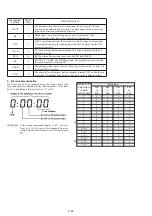
Page 128: ...emote commander can be disconnected hereafter 8 Press the push switch 1 knob in the direction of arrow which sets the machine into loading mode PB FF REW and CUE REV operations are possible 9 After completing all steps of above operation be sure to perform 4 Processing after operation 2 How to establish RECORD mode 1 Press pin of the push switch 2 ON state and keep the ON state by fixing with adhe...

Page 129: ...ss 00 set data 01 and press the PAUSE button 6 Select page F address 02 set data 03 and press the PAUSE button 7 Turn off the power supply once then turn it on 8 Connect an oscilloscope CH1 VC 188 board CN102 pin 1 External trigger VC 188 board CN102 pin 8 9 Playback the tracking alignment tape WR5 1NP NTSC WR5 1CP PAL 10 Check to see that RF waveform is flat at input and exit sides on oscilloscop...

Page 130: ... check 2 Servo system adjustment 1 SYNC level and BURST level adjustment 2 Switching position adjustment 3 Capstan FG offset adjustment 3 Playback frequency response characteristics adjustment 4 DEMD OUT level adjustment 5 YD OUT LEVEL adjustment 6 PB Chroma level check 7 PB Y out level adjustment 8 FE OSC check 9 Emphasis input level adjustment 10 Y FM deviation adjustment 11 Y FM carrier frequen...

Page 131: ...eration for SP WR5 5NSP Parts code 8 967 995 42 or WR5 4NSP Parts code 8 967 995 41 or WR5 9NS Parts code 8 967 995 23 for LP WR5 4NL Parts code 8 967 995 51 3 1 2 Precautions on adjustment The EVF electronic viewfinder is not necessary for video section adjustment Remove the following connector to remove the EVF 1 CF 44 board CN403 8 pin B W EVF model CF 44 board CN404 16 pin COLOR EVF model The ...

Page 132: ...tape use any type of tape for the checking purpose Note Tape type MP Metal particle tape Name Tracking WR5 1CP 1NP Video frequency response adjustment WR5 6C 6N Operation check SP mode WR5 5CSP 5NSP Operation check WR5 4CL 4NL Operation check WR5 9CS 9NS Record Mode Normal Normal Normal Normal Normal Tape Type MP MP MP MP MP Tape Speed SP SP SP LP SP Use Tape path adjustment Switching position adj...

Page 133: ...across 75 termination 3 1 6 Output level and impedance Video output Pin jack Output signal 1Vp p 75Ω unbalanced sync negative Audio output Pin jack Input level 7 5dBs across 47kΩ load Output impedance 2 2kΩ or less Color bar signal of PAL alignment tape Color bar signal of NTSC alignment tape PAL MODEL NTSC MODEL ...

Page 134: ...SYSTEM ADJUSTMENT 1 Power supply voltage check VC 188 board Mode Camera record Subject Any subject Measuring Equipment Digital voltmeter MT5V check Measuring Point CN301 pin º Specification Value 5 0 0 15Vdc DIG 3V check Measuring Point CN301 pin Specification Value 3 16 0 1Vdc AU 3 V check Measuring Point CN501 pin 5 Specification Value 3 18 0 1Vdc EVF 5V check camera mode Measuring Point CN301 p...

Page 135: ...ment position and turn on the UNREG power supply 2 6 00 01 After setting the data press the PAUSE button Preparation 3 F 02 03 After setting the data press the PAUSE button 4 Turn off the UNREG power supply once then turn it on Order Page Address Data Procedure 1 6 00 01 After setting the data press the PAUSE button 2 F 02 00 After setting the data press the PAUSE button 3 Turn off the UNREG power...

Page 136: ...r during capstan normal speed 40 FG error during drum startup 41 FG error during drum startup 42 FG error during normal rotation of drum 43 Not used 44 Phase error during normal rotation of drum 4 MSW code The lower digit data of the page F address E6 EA and EE indicate the MSW code mode switch code when an error occurs The upper digit data of the page F address E6 EA and EE indicate the MSW code ...

Page 137: ...e is it operating EJECT completed position If a cassette is ejected it stops at this position If mechanism moves in the loading direction the TG1 guide and the TG9 guide start moving The code during loading and unloading This code is output while the LS chassis is moving REW position The position to activate the REW and FR REV PB REC CUE REV and PAUSE position The pinch roller is pressed and the t...

Page 138: ...the data press the PAUSE button 4 6 11 01 After setting the data press the PAUSE button 5 F E4 EF 00 After setting the data press the PAUSE button 6 6 01 00 After setting the data press the PAUSE button 7 6 00 00 After setting the data press the PAUSE button End Order Page Address Date Procedure 1 Turn CAM POWER ON 2 Check LED 3 2 00 00 After setting the data press the PAUSE button 4 2 A0 10 Tally...

Page 139: ...dure 1 2 00 01 After setting the data press the PAUSE button 2 2 37 From the display data of each address it can be known 2F to 33 which key is being pressed Display data Address 2F KEY AD0 IC402 30 KEY AD1 IC402 31 KEY AD2 IC402 32 KEY AD3 IC402 37 PROGRAM AE IC402 00 0B STOP VC 188 board S302 TITLE S412 DATE S411 TIME S406 0C 27 FF VC 188 board S303 PICTURE EFFECT S413 BACK LIGHT S410 COUNTER RE...

Page 140: ... 02 to 04 on page 0 Note This data will be cleared when the button battery is removed reset Be sure to read the data before disassembling the set Order Page Address Data Procedure 1 2 00 02 After setting the data press the PAUSE button 2 7 0E 01 Individual operation of motors is approved 3 7 11 Motor can be operated individually by setting the above described data 4 Turn the main power 7 2V OFF No...

Page 141: ...tton of the adjusting remote commander 6 2 39 Read the data displayed on the adjustment remote commander This data is named Dref 7 F 2A After setting the data Dref and press thePAUSE button of the adjusting remote commander 8 Convert Dref into the decimal number The result decimal number is Dref Note 2 9 Calculate the following equation decimal calculation to obtain the following adjustment data d...

Page 142: ... Adjustment address 3E SYNC LEVEL 3F BURST LEVEL Specifications SYNC LEVEL A 300 10mV PAL A 286 10mV NTSC BURST LEVEL B 300 6mV PAL B 286 6mV NTSC Adjustment procedure Order Page Address Data Procedure 1 6 00 01 After setting the data press the PAUSE button Preparation 2 6 01 03 After setting the data press the PAUSE button 3 F 3E Change the data using the PLAY and STOP buttons until the SYNC LEVE...

Page 143: ... 4 Press the PAUSE button 5 F 22 Change the data with the PLAY and STOP buttons and minimize t1 6 Press the PAUSE button 7 Check that t1 satisfies the specified value If not repeat steps 3 to 6 in order 8 F 01 Raed the data of page F address 01 and record it 9 F 01 10 After setting the data Press the PAUSE button Forced LP head selection 10 F 25 80 Initial setting 11 F 25 Change the data with the ...

Page 144: ...nt Page F Adjustment Address 2B Specification Value Duty 50 1 5 Adjustment procedure Order Page Address Data Procedure 1 6 00 01 After setting the data press the PAUSE button Preparation 2 F 2B 80 After setting the data press the PAUSE button 3 F 2B Change data using PLAY and STOP buttons so that the duty ratio A B satisfies the specification 4 Press the PAUSE button 5 6 00 00 After setting the da...

Page 145: ...e PAUSE button Preparation 2 F 38 Change data using PLAY and STOP buttons to adjust the level ration between 3 5MHz level and 5 5MHz level of the PB RF waveform of channel 1a satisfies the specification Press the PAUSE button Playback mode 3 F 39 Adjust the channel 2a in the same way address 39 Press the PAUSE button Playback mode 4 F 01 Read the data of page F address 01 and record it 5 F 01 10 A...

Page 146: ...01 pin º or CN102 pin 6 Measuring Instrument Oscilloscope Adjustment Page F Adjustment Address 33 Specification Value A 0 50 0 01Vp p Adjustment procedure Fig 6 3 1 Order Page Address Data Procedure 1 6 00 01 After setting the data press the PAUSE button Preparation 2 F 33 Change data using PLAY and STOP buttons so that the Y signal level A satisfies the specification 3 Press the PAUSE button 4 6 ...

Page 147: ...djustment Page F Adjustment Address 3C Specification Value A 0 50 0 01Vp p Note Minimize the residual chroma to the smallest amplitude Adjustment procedure Related Adjustments Emphasis input level adjustment PB Y level adjustment Y FM carrier frequency adjustment Order Page Address Data Procedure 1 6 00 01 After setting the data press the PAUSE button Preparation 2 F 3C Change data using PLAY and ...

Page 148: ...ar segment of operation check tape Normal mode WR5 5CSP PAL WR5 5NSP NTSC Measurement Point CN102 pin 6 Measuring Instrument Oscilloscope Adjustment Page Adjustment Address Specification Value A 150 15mVp p BURST LEVEL Adjustment procedure Order Page Address Data Procedure 1 Playback the color bar segment of the normal mode alignment tape 2 Check that the burst signal level satisfies the specifica...

Page 149: ...terminal terminated in 75Ω Measuring Instrument Oscilloscope Adjustment Page F Adjustment Address 32 Specification Value A 1 00 0 05Vp p Adjustment procedure Order Page Address Data Procedure 1 6 00 01 After setting the data press the PAUSE button Preparation 2 Playback the color bar segment of the normal alignment tape 3 F 32 Change data using PLAY and STOP buttons so that the playback signal lev...

Page 150: ...cilloscope and frequency counter Adjustment Page Adjustment Address Specification Value A 7 0Vp p or more MP mode A 6 0 1 0Vp p ME mode f 7 2 0 5MHz MP ME mode Adjustment procedure Order Page Address Data Procedure 1 Insert a normal MP type tape 2 Make a recording 3 Check that the FE signal level satisfies the specification 4 Check that the FE signal frequency satisfies the specification 5 Insert ...

Page 151: ...tion Value A Vo 0 96 500 mVp p 2 Adjustment procedure Order Page Address Data Procedure 1 6 00 01 After setting the data press the PAUSE button Preparation 2 6 01 Read the data of page 6 address 01 and record it 3 6 01 47 After setting the data press the PAUSE button 4 Measure amplitude of the VIDEO OUT The measured value is Vo V 5 F 31 Change data using PLAY and STOP buttons so that the Y signal ...

Page 152: ...re 1 Insert a normal MP type tape 2 6 00 01 After setting the data press the PAUSE button Preparation 3 6 01 Read the data of page 6 address 01 and record it 4 6 01 47 After setting the data press the PAUSE button 5 Shoot and record the color bar chart The video out level at that setup is Vo 6 Playback the recorded signal 7 Compare the playback signal level A with the specification value If the sp...

Page 153: ...ment Point IC201 pin Measuring Instrument Frequency counter Oscilloscope Adjustment Page F Adjustment Address 30 Specification Value 4 20 0 01MHz Adjustment procedure Order Page Address Data Procedure 1 6 00 01 After setting the data press the PAUSE button Preparation 2 6 01 43 After setting the data press the PAUSE button 3 F 30 Change data using PLAY and STOP buttons so that the carrier frequenc...

Page 154: ... output terminal terminated in 75Ω Measuring Instrument Oscilloscope Adjustment Page F Adjustment Address 34 Specification Value Minimizes the chroma component A in the following diagram Adjustment procedure PAL MODEL NTSC MODEL Order Page Address Data Procedure 1 6 00 01 After setting the data press the PAUSE button Preparation 2 F 34 Change data so that the chroma component A is minimized 3 Pres...

Page 155: ...A 155 5mVp p NTSC Adjustment procedure Note Use the MP type tape If an oscilloscope has the bandwidth limiting switch set to on position Order Page Address Data Procedure 1 6 00 01 After setting the data press the PAUSE button Preparation 2 Insert the MP tape to establish record mode 3 6 01 Read the data of page 6 address 01 and record it 4 6 01 43 After setting the data press the PAUSE button 5 F...

Page 156: ...re Vo 714 Order Page Address Data Procedure 1 Shoot the all white pattern to the full picture frame 2 6 00 01 After setting the data press the PAUSE button Preparation 3 6 01 Read the data pf page 6 address 01 and record it 4 6 01 45 After setting the data press the PAUSE button 5 Measure the chroma output level of the VIDEO OUT connector Obtain the average value of three points beginning middle e...

Page 157: ...EE OUTPUT LEVEL CHECK Mode Record signal CN501 pin 4 INPUT Left CN501 pin 2 INPUT Right 400 Hz 38 dBs Audio input from CN501 pin 4 2 Measurement Point AUDIO output terminal Left Right no load Measuring Instrument Audio level meter Specification Value 7 5 2 0dBs Check procedure Order Procedure 1 Check that 400 Hz signal level satisfies the specification Alignment tape MONO model WR5 5CSP PAL WR5 5N...

Page 158: ...Order Page Address Data Procedure 1 Select the same vertical sensitivity of CH1 and CH2 of oscilloscope 2 Set the oscilloscope to ADD mode and set CH2 to INV mode 3 6 00 01 After setting the data press the PAUSE button Preparation 4 F 2C Change data using PLAY and STOP buttons so that the audio level difference A is minimized 5 Press the PAUSE button 6 6 00 00 After setting the data press the PAUS...

Page 159: ... Order Page Address Data Procedure 1 Select the same vertical sensitivity of CH1 and CH2 of oscilloscope 2 Set the oscilloscope to ADD mode and set CH2 to INV mode 3 6 00 01 After setting the data press the PAUSE button Preparation 4 F 2D Change data using PLAY and STOP buttons so that the audio level difference A is minimized 5 Press the PAUSE button 6 6 00 00 After setting the data press the PAU...

Page 160: ... 5NSP NTSC STEREO model WR5 9CS PAL WR5 9NS NTSC Measurement Point AUDIO output terminal Left Right Measuring Instrument Audio level meter Adjustment Page F Adjustment Address 2E Specification Value Distortion 1 or less Adjustment procedure Order Page Address Data Procedure 1 6 00 01 After setting the data press the PAUSE button Preparation 2 F 2C Change the data with the PLAY and STOP buttons and...

Page 161: ...terminal Left Right Measuring Instrument Audio level meter using IHF A curve weighting filter Specification Value 65dBs or less Note Before making short circuit between CN501 pin 3 and pin 4 pin 3 and pin 2 STEREO model only remove the flexible board from CN501 Check procedure Order Procedure 1 Insert a shorting to pin 3 and pin 4 pin 3 and pin 2 STEREO model only as CN501 2 Make recording 3 Remov...

Page 162: ...FRARED TRANSMIT CIRCUIT ADJUSTMENT IR MODEL 5 1 PREPARATIONS 1 Equipment connection Resistors 75Ω 1 247 804 11 270Ω 1 249 410 11 330Ω 1 249 411 11 47kΩ 1 249 437 11 2 Switch setting IR switch VC 188 board S308 ON ...

Page 163: ...ation Value 11 83 0 05MHz Adjustment procedure IR 28 BOARD SIDE A Order Page Address Data Procedure 1 6 00 01 After setting the data press the PAUSE button Preparation 2 6 01 Read the data pf page 6 address 01 and record it 3 6 01 43 After setting the data press the PAUSE button 4 F 5C Change data using PLAY and STOP buttons so that the carrier frequency satisfies the specification Record mode 5 P...

Page 164: ...Vo 0 05Vp p Adjustment procedure Order Page Address Data Procedure 1 6 00 01 After setting the data press the PAUSE button Preparation 2 6 01 Read the data pf page 6 address 01 and record it 3 6 01 47 After setting the data press the PAUSE button 4 Record the output level A of the VIDEO OUTPUT terminal of the unit as Vo Vo 1 0 0 05Vp p 5 F 5D Change data using PLAY and STOP buttons so that the Y s...

Page 165: ...nt Audio level Adjustment Page F Adjustment Address 5E Specification Value 7 5 1 0dBs Adjustment procedure Order Page Address Data Procedure 1 6 00 01 After setting the data press the PAUSE button Preparation 2 Input the audio signal of 400 Hz 66dBs to the EXT MIC terminal L ch and R ch of the unit 3 F 5E Press the PLAY and STOP buttons until the audio signal level of both L ch and R ch satisfies ...

Page 166: ......

Page 167: ...6PK TR507 TR916 NTSC CCD TR501E TR502E TR503E TR506E TR620E TR720E TR740E PAL 258 Sony Corporation Personal A V Products Company 97B16102 1 Printed in Japan 1997 2 Published by Quality Engineering Dept Osaki East 9 973 938 11 ...

Page 168: ......

Page 169: ......

Page 170: ......

Page 171: ......

Page 172: ......

Page 173: ......

Page 174: ......

Page 175: ......

Page 176: ......

Page 177: ......

Page 178: ......

Page 179: ......

Page 180: ......

Page 181: ......

Page 182: ......

Page 183: ......

Page 184: ......

Page 185: ......

Page 186: ......

Page 187: ......

Page 188: ......

Page 189: ......

Page 190: ......

Page 191: ......

Page 192: ......

Page 193: ......

Page 194: ......

Page 195: ......

Page 196: ......

Page 197: ......

Page 198: ......

Page 199: ......

Page 200: ......

Page 201: ......

Page 202: ......

Page 203: ......

Reviews: