background image

HBD-E2100/E3100/E3200/E4100/E6100

34

Power Check Flow (2/2)

C

heck that 

so

und is 

outputted 

nor

mally.

Ch

ec

th

at

 [A

ud

io

 S

et

tin

gs

]-[A

ud

io

 o

ut

pu

t] in

 th

e m

en

u

sc

re

en is

 “Speaker

”.

C

heck 

that the dr

ive 

is 

oper

ating 

nor

m

ally.

C

heck that 

each pow

er 

supply

 is

 s

upplied to 

the 

audio

block.

C

heck that 

so

und is 

nor

m

ally outputted f

rom 

each

sp

ea

ke

r.

Ref

er

 to 

the 

“Po

we

r C

he

ck

 Flo

(1/2)

” on 

page 

33.

Ref

er

 to 

the “2-1. Flow

 of

 dr

ive 

se

ction check” on 

page

on or

iginal 

se

rvice manual.

C

heck 

that a 

pictur

is

 outputted nor

mally.

C

heck that 

each s

peaker

 is

 connected 

nor

mally.

Fr

ont/C

enter

/Sur

ro

und/Subw

oof

er

C

heck 

that the PWM s

ignal is

 outputted 

from 

the

fo

llow

ing pins

.

AMP 

board 

IC3001 

pin 

39, 

40, 

48, 

49, 42, 43, 54, 55

C

heck 

that the s

ignal is

 outputted 

from 

the 

fo

llowing

pins

.

AMP board 

IC3102

pin 

10, 11 (SP 

FRO

N

T R)

pin 

16, 17 (SP 

FRO

N

T L)

Pin 2, 

3, 

8, 

(S

SU

BWOOFE

R)

O

ptimize the 

speaker

 s

ettings

.

C

heck 

that the s

ignal is

 outputted 

from 

the 

fo

llowing

pins

.

AMP board 

IC3302

pin 10, 11, 16, 17 (SP CENTER) pin 

2, 

3 (S

SUR R)

Pin 

8, 9 (S

SU

R L)

No

No

No

No

No

No

No

No

No

Ref

er

 to 

the 

“HDMI C

hec

Flow” 

on page 35.

Per

for

m and check [

Audio 

Settings

] -

[S

peaker

 Settings

] - [T

es

t T

one]

 in the menu

sc

re

en

, o

r re

in

se

rt t

he

 sp

ea

ke

r c

ab

le

s.

Exchange the 

IC

3001.

Part N

o. 

6-718-103-01

Description IC 

TAS

5538DGGR

Exchange the 

IC

3102.

Part N

o. 

6-719-138-01

Description IC 

ST

A516BF1

3T

R

-A

No

Exchange the 

IC

3302.

Part No. 6-719-138-01 Description IC 

ST

A516BF1

3T

R

-A

A

Ye

s

Ye

s

Ye

s

Ye

s

Ye

s

Ye

s

C

heck 

that the s

ignal is

 input 

to 

AMP 

board 

IC3001.

Pin 22, 23, 24, 25, 27

No

Change FFC. Insert to AMP CN3505

Ye

s

Ye

s

Ver. 1.5

Summary of Contents for HBD-E2100

Page 1: ... R 75 W per channel at 3 ohms 1 kHz Photo HBD E3100 Center 150 W at 6 ohms 1 kHz Subwoofer 150 W at 6 ohms 80 Hz Inputs Analog AUDIO IN Sensitivity 1 V 400 mV Inputs Digital TV Audio Return Channel OPTICAL Supported formats LPCM 2CH up to 48 kHz Dolby Digital DTS HDMI Section Connector Type A 19 pin BD DVD CD System Signal format system NTSC PAL except US PX and Canadian models NTSC US PX and Cana...

Page 2: ...a is a trademark of Verance Corporation Copyright 2004 2010 Verance Corporation All rights reserved by Verance Reverse engineering or disassembly is prohibited Windows Media is either a registered trademark or trademark of Microsoft Corporation in the United States and or other countries This product is protected by certain intellectual property rights of Microsoft Corporation Use or distribution ...

Page 3: ...ny one of three methods 1 A commercial leakage tester such as the Simpson 229 or RCA WT 540A Follow the manufacturers instructions to use these instruments 2 A battery operated AC milliammeter The Data Precision 245 digital multimeter is suitable for this job 3 Measuring the voltage drop across a resistor by means of a VOM or battery operated AC voltmeter The limit indication is 0 75 V so analog m...

Page 4: ...7 Schematic Diagram AMP Board 2 3 54 6 18 Schematic Diagram AMP Board 3 3 55 TABLE OF CONTENTS 6 19 Printed Wiring Board PANEL Board 56 6 20 Schematic Diagram PANEL Board 57 6 21 Printed Wiring Board KARAOKE Board SP RU 58 6 22 Schematic Diagram KARAOKE Board SP RU 58 6 23 Printed Wiring Board POWER KEY Board 58 6 24 Schematic Diagram POWER KEY Board 58 7 EXPLODED VIEWS 7 1 Case Section 76 7 2 Fro...

Page 5: ...01 305 A HLX 513 Single Layer NTSC J 2501 306 A HLX 514 Dual Layer NTSC J 6090 077 A HLX 506 Single Layer PAL J 6090 078 A HLX 507 Dual Layer PAL TEST DISC Note Refer to the service manual of BDP BX1 S350 Part No 9 883 989 1 page 1 3 to 1 14E for the use of BLX 104 204 Operation and Display 1 BLX 104 Procedure 1 Select 23 976Hz 1080p 2 Play 4 Motion picture 3 Check whether player can play back or ...

Page 6: ...struction by ESD 1 2 Jig Digital camera Recommend with macro mode USB memory PC Barcode decoder Refer to 1 3 Barcode decoder BDPRdec 1 3 Barcode decoder BDPRdec Jig name BDPRdec exe Release 2011 8 25 Version 3 0 0 0 Software contents BDPRdec exe Barcode decoder software SavePath ini Decoded file destination setting file Ini tial destination is C BD BuData txt TasmanBars dll Decode dll Uninst exe U...

Page 7: ... No 1 846 349 61 and replace it when it has been damaged Then confirm whether this unit operates normally Confirm F201 F202 F203 on the MB1002 board and replace it when it is open Confirm whether the optical device IOP is normal in the service mode Refer to 2 2 Flow of optical device IOP check Replace the optical device KEM480AAA Refer to 3 Optical device KEM480AAA replacement NO OK YES YES YES NO...

Page 8: ...d make the text data File name BuData txt 5 Save the text data to USB memory 6 Connect USB memory with front USB connector on this unit and turn the power on 7 Press the FUNCTION button on the remote commander to select BD DVD 8 Press the buttons on the remote commander in order of DISPLAY 0 2 1 SUBTITLE and enter the service mode 9 Press the buttons on the remote commander in order of 8 1 ENTER a...

Page 9: ...s and Status Write Successfull Screen 3 9 Enter RETURN to the selection of test category Diag Category Bluetooth Device Test Diag Category Bluetooth Device Test 1 Bluetooth Enable 2 Bluetooth Disable 3 Write Bluetooth device address to Registry 4 Bluetooth Inquiry Test Status Bluetooth Enable Successful HELP UP DOWN ENT RET Screen 1 Screen 2 Screen 3 Diag Category Bluetooth Device Test 1 Bluetooth...

Page 10: ...ds of respective capacitors Switching regulator C207 C201 C402 C503 C504 SWITCHING REGULATOR Conductor Side To both ends of each capacitor 800 2 W C201 C207 C402 C504 C503 NOTE OF REPLACING THE IC3102 AND IC3302 ON THE AMP BOARD AND THE COMPLETE AMP BOARD When IC3102 and IC3302 on the AMP board and the complete AMP board are replaced it is necessary to spread the compound GREASE G 747 1KG Part No ...

Page 11: ...t to the router or the hub etc with the LAN cable 2 Press the HOME button on the remote commander to enter the home menu 3 Press the m M buttons on the remote commander to select Network Settings Internet Settings and press the button on the remote commander 4 Press the m M buttons on the remote commander to select Wired Setup and press the button on the remote com mander 5 Press the m M buttons o...

Page 12: ...iew Note Push after it inserts it in this hole well MB1002 board AMP board BD drive BPX 7 POWER KEY board KARAOKE board SP RU NON KARAOKE board EXCEPT SP RU PANEL board RC S801 A WW switching regulator SWR1 3L392W 1 US CND AEP UK SAF SP TW AUS TH CH 3L392W E3 E51 PX EA E12 E32 RU MX6 AR card WLAN BT COMBO Abbreviation AR Argentina model AUS Australian model CH Chinese model CND Canadian model E3 2...

Page 13: ... SET 2 2 HOW TO BEND FFC Page 14 2 11 OPTICAL PICK UP BLOCK KEM480AAA WIRE FLAT TYPE Page 20 2 7 POWER KEY BOARD WLAN BT COMBO CARD KARAOKE BOARD SP RU PANEL BOARD Page 17 2 9 AMP BOARD Page 18 2 10 SWITCHING REGULATOR SWR1 Page 19 2 6 BD DRIVE BPX 7 Page 16 2 4 PANEL LOADING ASSY Page 15 2 8 MB1002 BOARD Page 18 2 5 FRONT PANEL ASSY Page 16 Ver 1 5 ...

Page 14: ...N02 25 mm 45º 45º 18 mm 22 mm 235 mm The upper side is contact side The upper side is contact side wire flat type 21 core length 305 mm Ref No 57 SP RU MB1002 board CN803 PANEL board CN01 30 mm 45º 45º 10mm 20 mm 235 mm The upper side is contact side The upper side is contact side The upper side is contact side The upper side is contact side wire flat type 8 core length 260 mm Ref No 52 40 mm 220 ...

Page 15: ...ur screws BV3 3 CR 7 case 2 four screws BV3 3 CR 3 five claws A A 5 4 6 1Insert the clip etc tray BD drive Insert the clip etc processed to the length of 8 cm or more in the hole on the side of the chassis and push 8 cm or more hole Side view Top view Note Push after it inserts it in this hole well 3four claws 4panel loading assy 2 Ver 1 5 ...

Page 16: ... MB1002 board front side 63 58 E3100 E4100 E6100 E2100 2 5 FRONT PANEL ASSY Abbreviation RU Russian model SP Singapore model 2 6 BD DRIVE BPX 7 4 four screws BV3 3 CR 8 BD drive BPX 7 7 sheet sound 5 boss 6 1 flexible flat cable 45 core CN501 2 wire flat type 9 core CN660 3 wire flat type 5 core CN670 Note When you install the BD drive BPX 7 please match the position of the boss two places Ver 1 5...

Page 17: ...5 core CN02 EXCEPT SP RU G G D F F F D E E E D SP RU EXCEPT SP RU LUH VHWWLQJ LUH VHWWLQJ LUH VHWWLQJ front side front side front side switching regulator SWR1 switching regulator SWR1 switching regulator SWR1 MB1002 board MB1002 board MB1002 board harness USB 0 two screws BV3 3 CR qa PANEL board 2 7 POWER KEY BOARD WLAN BT COMBO CARD KARAOKE BOARD SP RU PANEL BOARD Abbreviation RU Russian model S...

Page 18: ... sink AMP 5 1CH 4 three screws BV3 3 CR 6 two screws BV3 3 CR 7 AMP board switching regulator SWR1 LUH VHWWLQJ AMP board 1 CN201 2P 2 tape 3 wire flat type 24 core CN707 4 CN202 8P 5 five screws BV3 3 CR 6 one screw BV3 3 CR 8 MB1002 board 7 one screw B 3 u 5 2 8 MB1002 BOARD 2 9 AMP BOARD Ver 1 5 ...

Page 19: ...r side switching regulator SWR1 2 10 SWITCHING REGULATOR SWR1 Abbreviation AR Argentina model AUS Australian model CH Chinese model CND Canadian model E3 240 V AC area in E model E12 220 240 V AC area in E model E32 110 240 V AC area in E model E51 Chilean and Peruvian models EA Saudi Arabia model MX6 Latin American model PX PX model RU Russian model SAF South African model SP Singapore model TH T...

Page 20: ...7 8 9 2 two claws 3 holder chuck assy T qd wire flat type 5 core qf tape FFC Bottom view loading assy T 8 9 cover drive 1 flexible flat cable 45 core 6 wire flat type 5 core Fold Fold 2 Through the hole 3 wire flat type 9 core 4 Through the hole terminal face terminal face loading assy T Under the guide Fold area Under the guide QVWDOODWLRQ RI IOH LEOH IODW FDEOH FRUH ZLUH IODW W SH FRUH DQG ZLUH ...

Page 21: ...icator tube are lighted up This operation is repeated 4 In the state of step 3 press the VOL button on the remote commander and model information is displayed on the fluores cent indicator tube Each time the VOL button on the remote commander is pressed the display changes from destination information STR version special mode in this order and returns to the model information display 5 In the stat...

Page 22: ...ation of the unit Displays information such as the software version drive infor mation etc EMC Test Mode Not used Drive Write drive OP data and check drive HDD Mode Not used 6 The message Close appears and press the button on the remote commander 7 Select Reset to Factory Default Settings and press the button on the remote commander 8 Select All Settings and press the button on the remote commande...

Page 23: ...udio Test udio output test udio Input Test XGLR QSXW 7HVW LUHOHVV 1 7HVW Only wireless model used 0 7HVW 0RGH Not used Drive Write drive OP data and check drive Start Update 6WDUW GLVF XSJUDGH Start Initialize QLWLDOL H GHIDXOW VHWWLQJ IRU WKH XQLW LDJ 7HVW 0LF 7HVW Not used 0 QSXW 7HVW Not used Transcorder Test Not used Service 0ode 0enu 1 DiaJ 2 LoJ 3 Factory Initialize 4 Network 5 Version Up 6 ...

Page 24: ...turns to selection of test category List of test categories Device Test Video Test Audio Test Audio Input Test Wireless LAN Test Mic Test Not used HDMI Input Test Not used Transcorder Test Not used Bluetooth Device Test Device Test List of devices USB Host USB media check front Only one time 5 Diag Video Audio Test This screen performs video and audio tests Screen 1 When video test category is sel...

Page 25: ... category RETURN Returns to the service top menu Screen 2 Wireless LAN test 1 Show WLAN Hwinfo 2 Connect to AccessPoint 3 Start display RSSI value 4 Start Ping Test Operation M m Selects the test Executes the test RETURN Returns to selection of test category Screen 2 Select 1 Show WLAN HwInfo Viewing the display Serial Serial Number Hard Hardware Version Mac Mac Address Screen 3 Select 2 Connect t...

Page 26: ...ooth Disable Successful Fail Bluetooth Disable Fail Screen 4 Select 3 Store Bluetooth device address to Registry Display will show Bluetooth device address xx xx xx xx xx xx Viewing the Status display if Successful Write Successful Fail Write Fail Category Wireless LAN Test 1 Show WLAN HwInfo 2 Connect to AccessPoint 3 Stop Display RSSI Value 4 Start Ping Test RSSI Value 60 HELP UP DOWN ENT RET Sc...

Page 27: ... Moves to the next page RETURN Returns to the screen Screen 1 that selects the log type RED Writes the log contents to an USB memory device Viewing the log display Error Log 174 2010 01 01 00 00 08 ErrCode 0902A4053002 Index number Date Time Error code About copying log to USB memory device Press the RED button in each log display screen with the USB memory device inserted into the unit Note Pleas...

Page 28: ...ct Ifconfig test m Ping execution preparation RETURN Returns to the top menu of the service mode Screen 2 The IP address of the Ping point is set up IP address input mode When Ping to is reversed the button is pressed and IP is inputted Operation Finish to input RETURN Finish to input Finish to input and Select Ifconfig Test 0 to 9 Input Character sting 0 9 Screen 3 Ping Test Active When START is ...

Page 29: ...c Information Operation Drive information delta IOP of a drive is measured and wireless device information not used displayed go to Screen 2 RETURN Returns to the top menu of the service mode Screen 2 Drive and Wireless Information Menu Operation Basic Information displayed go to Screen 1 RETURN Returns to the top menu of the service mode When delta IOP is measured it becomes impossible to use the...

Page 30: ... operating check Service is only use Drive OP data write to rewrite OP data after change of new CPU System Information Sequence Number MAC IP Model Main LSIname Destination IF con Block0 Version Bootloader Version Host Main Version MicroBE Version Host Sub Version Middleware Version ADSP Version ADSP Coeff Version HELP RET RIGHT Screen 1 System Information CD DIOP DVD DIOP WLAN module hw version W...

Page 31: ...r player can play back or not Check the sound output 4 HLX 513 514 NTSC HLX 506 507 PAL Procedure 1 After displayed Main Menu select 1 Video Signal 2 Play 1 Color bar 100 Check the picture and sound output 3 Return to Menu 4 Play Demonstration 4 3 or Demonstration 16 9 Check the picture and sound output 1 2 Playback operation confirmation Confirm operation in each signal output mode of test disc B...

Page 32: ...odulation 1 kHz ANT input 35 dBu EMF Note Please use 75 ohm coaxial cable to connect SG and the set You cannot use video cable for checking Please use SG whose output impedance is 75 ohm 3 Set to FM tuner function and scan the input FM signal with automatic scanning 4 Confirm that input Frequency of A B and C detected and auto matic scanning stops The stop of automatic scanning means The station s...

Page 33: ...25 PCONT_FL Yes The power is turned on A No Yes Protect mode happened PROTECT display appears on fluorescent tube No Yes Check that harness is inserted normally at CN101 Remove harness of CN101 CN4 FFC CN3505 Measure switching supply board CN101 pin4 pin1 normal voltage 30V Yes Yes AMP board damage Exchange the complete AMP board Check that harness is inserted normally at CN301 and CN202 When harn...

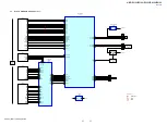
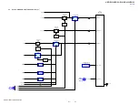
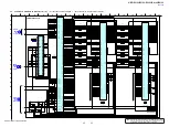
Page 34: ...40 48 49 42 43 54 55 Check that the signal is outputted from the following pins AMP board IC3102 pin 10 11 SP FRONT R pin 16 17 SP FRONT L Pin 2 3 8 9 SP SUBWOOFER Optimize the speaker settings Check that the signal is outputted from the following pins AMP board IC3302 pin 10 11 16 17 SP CENTER pin 2 3 SP SUR R Pin 8 9 SP SUR L No No No No No No No No No Refer to the HDMI Check Flow on page 35 Per...

Page 35: ...on the menu screen Refer to the Power Check Flow 1 2 on page 33 Check that the input voltage of the following pin is 3 3V MB1002 board IC408 pin 1 CONT Refer to the Power Check Flow 1 2 on page 33 to check on power control signal for PCONT_3 Refer to the 2 1 Flow of drive section check on page 7 on original service manual Exchange the IC408 Part No 6 718 999 01 Description IC MM1839A50NRE Check th...

Page 36: ... 1 US CND AEP UK SAF SP TW AUS TH CH 3L392W E3 E51 PX EA E12 E32 RU MX6 AR Abbreviation AR Argentina model AUS Australian model CH Chinese model CND Canadian model E3 240 V AC area in E model E12 220 240 V AC area in E model E32 110 240 V AC area in E model E51 Chilean and Peruvian models EA Saudi Arabia model MX6 Latin American model PX PX model RU Russian model SAF South African model SP Singapo...

Page 37: ...A A HAVC P3 VC_PD AUX1 P14 THERMO FETRAYPWM P39 FEFMO2 P35 FEFMO P34 FEGIO0 P43 FEGAINSW3 P29 FEFG P41 CN380 USB_DM_P1 P55 USB_DP_P1 P56 CN52 3 1 2 TXVP_1 P212 COIL MOTOR DRIVER IC601 XFG 12 SOMI 17 SIMO 16 SLED1_P LOAD_P 1 27 LOAD_N 26 SLED1_N 2 SLED2_P 4 SLED2_N 5 W V U COMMON U 43 V 45 W 47 MCOM 49 TR TD TRK_P 37 TRK_N 38 FD1 FR1 FCS_P 39 FCS_N 40 FD2 FR2 TLT_P 36 TLT_N 35 SCLK 15 RDY 13 FEGIO4...

Page 38: ... 16 ALE CLE 19 WP IO1 IO8 NAND_RESET RRESET P134 L3 L2 WE WE M2 BA0 N8 BA1 M3 BA2 CS K3 J3 CAS RAS K9 CKE J7 CK K7 CK D3 C7 DMU DQSU B7 E7 DQSU DML K1 ODT F3 DQSL G3 DQSL T2 RESET RDQ16 RDQ31 MAIN SECTION Page 39 C MAIN SECTION Page 39 A MAIN SECTION Page 39 B CH0_P P221 SPDIF_IN1 P64 CH0_M P220 7 9 CH1_P P223 CH1_M P222 4 6 CH2_P P225 CH2_M P224 1 3 CLK_P P219 CLK_M P218 10 HTPLG TMDS DATA0 TMDS ...

Page 39: ...T2 PCONT1 PCONT1 36 BD_SDO IF_SDI IF_SDI 76 JIG_MODE1 82 BD_SDI IF_SDO IF_SDO 75 BD_CLK 77 BD_CS UPG_STATUS OPWRSB FE_EJECT 78 85 83 84 PCONT3 ND01 VACUUM FLUORESCENT DISPLAY 3 FL_DOUT 5 FL_CLK 68 FL_CS SIRCS_IN REMOTE CONTROL SIGNAL RECEIVER IC01 1 AC_CUT 18 UNSW 12V VOLTAGE DETECT IC803 DCDC 5V AC CUT DRIVER Q209 S41 KEY0 EJ PANEL 5 5V S05 S08 KEY1 89 KEY1_EJ 88 S01 S04 KEY2 KEY2_EJ 87 X801 8MHz...

Page 40: ... POWER AMP IC3102 IN2A OUT1B 1N2B OUT1B 31 32 29 1N1A 30 25 IN1B xPWRDN 27 xFAULT 26 xTRISTATE POWER AMP 33 TAS5538_SDA 34 TAS5538_SCL IC3302 IN2A 1N2B 31 32 65 DRIVER_SD POWER_DET 40 PCONT STA516 50 STA516_XPDN AMP_D1 AMP_MCK AMP_BCK AMP_LRCK 25 42 43 SDIN2 55 54 20 21 16 XRESET XMUTE SDA SCL 19 PWM_P_5 PWM_M_6 37 VALID PWM_P_3 PWM_M_3 AMP_D2 27 SDIN4 OVERLOAD DETECTION Q3202 L3103 L3303 SUR R SU...

Page 41: ... 12 3 SW1 EN2 VIN1 ICUNSW12V EN_POWER 3 3V 5V REG 1 2V 3 3V REG PANEL 5 5V PCONT3 PCONT2 PCONT1 DC DC CONVERTER IC203 1 14 3 SW1 SW2 VIN1 5V VOLTAGE CONTROL Q206 4 5 3 F203 F201 F802 UNSW 5 5V FE_SW12V 12V VOLTAGE CONTROL Q205 4 5 3 OVERLOAD DETECTION Q202 3 3V VOLTAGE CONTROL Q204 4 5 3 PVDD_CONT OVERLOAD DETECTION Q207 OVERLOAD DETECTION Q203 PVDD_VOL_SEL EJ 99 3 3V REG IC805 5V REG IC710 5 4 3 ...

Page 42: ...re omitted E Q B These are omitted C E Q Lead layouts surface CSP Chip Size Package Lead layout of conventional IC Replacement of IC102 and IC103 on the MB1002 board used in this unit requires a special tool Note When the AMP board is replaced spread the compound referring to NOTE OF REPLACING THE IC3102 AND IC3302 ON THE AMP BOARD AND THE COMPLETE AMP BOARD on servicing notes page 10 A B Line B B...

Page 43: ...8 R521 R909 R522 R331 R332 R910 R911 R913 CN706 CN707 2 1 24 23 R724 R531 R725 R726 R533 R727 C303 R920 C115 R733 C503 R734 C504 C311 X301 C505 JL101 C312 C506 JL102 C313 JL103 C314 JL104 JL105 JL106 R353 JL107 JL108 JL109 C320 JL110 C321 JL111 C516 JL112 JL113 C518 C130 JL114 C519 JL115 JL116 JL117 JL118 X701 JL501 R365 JL119 JL502 JL503 JL504 JL505 C521 JL506 JL507 C523 C717 JL508 C524 C330 JL12...

Page 44: ...17 JL818 C259 JL819 R873 R874 R876 JL820 C261 JL821 C262 D202 K A C263 C264 CL1200 JL825 JL827 RB107 R884 RB108 RB109 RB302 RB110 RB111 C662 Q703 D804 R101 R103 R106 R107 CL596 CL597 JL883 JL884 JL885 JL886 JL887 R304 R115 R116 R316 R707 R708 R1010 R709 R900 R901 R716 R717 R718 R719 C108 R914 C109 R918 C118 R926 R927 R928 R738 C120 R739 C315 C121 C316 C122 C317 C123 C318 R740 R741 JL301 C706 JL302...

Page 45: ...3 JL1104 JL1105 JL1106 JL1013 JL1010 JL1008 JL1014 C1002 0 1 JL1001 JL1004 C1001 0 001 JL1012 JL1007 JL1006 JL1011 NFWEN JL1002 3 3k R1001 C1003 0 1 1 NC 2 NC 3 NC 4 NC 5 NC 6 NC 7 8 9 10 NC 11 NC 12 Vcc 13 Vss 14 NC 15 NC 16 CLE 17 ALE 18 19 20 NC 21 NC 22 NC 23 NC 24 NC 25 NC 26 NC 27 NC 28 NC 29 IO1 30 IO2 31 IO3 32 IO4 33 NC 34 NC 35 NC 36 Vss 37 Vcc 38 NC 39 NC 40 NC 41 IO5 42 IO6 43 IO7 44 I...

Page 46: ... JL214 JL219 JL220 CN201 2P DC FAN DC FAN 1k R247 JL218 JL217 IC201 BD00GA3WEFJ E2 DC FAN DRIVER 1 2 3 4 8 7 6 5 9 C254 0 001 C251 0 01 L206 2 2uH C244 10 C252 22 C245 10 JL221 C250 0 001 8 2k R258 C253 22 47k R259 10k R260 12k R264 DCDC5V 3 3 R263 C257 10 C259 10 C216 10 C238 0 01 C261 0 01 C262 0 01 C263 0 01 C264 0 01 L208 2 2uH L209 2 2uH 5 6k R268 68k R269 IC203 TPS54295PWPR 1 2 3 4 5 6 7 8 1...

Page 47: ... 1 C318 0 1 C322 0 1 C323 0 1 C324 0 1 C325 CN301 6P JL304 JL306 JL303 JL301 JL305 JL302 RB302 10k R316 100k R318 10k IC101 2 3 CXD90019R BA IC101 BD DECODER 0 1 C326 1 C327 1 C328 0 1 C330 10p C331 100k R331 1 8k R332 0 1 C381 24k R385 5 1k R395 10 C380 0 1 C390 10 C384 0 001 C303 27MHz X301 12p C332 1 4 2 3 1 C359 1 C358 10 C357 0 1 C356 0 1 C352 0 1 C353 0 1 C351 10 C350 100 R353 JL320 JL317 JL...

Page 48: ...54 FVREF P3 HAVC P34 FEFMO P35 FEFMO2 P37 FEFMO3 P38 FEFMO4 P24 FOO P25 TRO P40 FEDMO P26 TLO P53 FETRAYIN_ P39 FETRAYPWM P41 FEFG P249 AVDD12_1 P22 AVDD12_2 P4 AVDD33_1 P23 AVDD33_3 P250 RSTI P43 FEGIO0 P44 FEGIO1 P54 FEGIO3 P49 FEGIO4 P45 FEGIO5 P48 FEGIO6 P47 FEGIO7 P50 FEGIO9 P51 FEGIO10 P52 FEGIO11 F RF RF 5 0V SCLK SEN_LDD A GND 5 0V MODE_B GND THERMO SDIO G D GND TD GND 8 0V TR FD2 5V_PD FR...

Page 49: ...PDIF_IN AOBCLK AOMCLK AOLRCK AOSDATA0 AOSDATA1 AOSDATA2 MICIN C751 10 100 R786 22 R788 ST_RDS_INT L704 47nH C738 CL713 C742 47p C743 68p I2C_DATA_TUNER C737 1 X701 12MHz 22 R787 CL714 10k R785 100 R789 CN706 2P GND RF KA5V_IN I2C_CLK_TUNER CL715 L703 47nH IC703 SN74LV4052APWR 1 Y0 2 Y2 3 Y 4 Y3 5 Y1 6 INH 7 VEE 8 VSS 9 B 10 A 11 X3 12 X0 13 X 14 X1 15 X2 16 VDD CN707 24P 3 3VA TAS5538_SCL 3 3VA TA...

Page 50: ...16 _XPDN 51 TAS5538 _XRST 52 TAS5538 _XMUTE 53 XWAMUTE 54 TS_SDA 55 TS_SCL 56 NO USE 57 MIC CLK 58 MIC_DATA 59 Front_End_Reset 60 VCC2 61 NJU72341_POWER 62 VSS 63 PLUG_DET MIC IN 64 BT_LED NJ 65 DRIVER_SD POWER_DET 66 BD_TEMP EJ 67 STA516_TH_WARN 68 FL_CS 69 ASEL0 70 ASEL1 71 WOL_WLAN 72 NFC_RFDET 73 ST_RDS_INT 74 NAND_RESET 75 76 77 78 79 80 81 82 83 84 85 86 87 88 89 90 91 92 93 94 95 96 97 98 1...

Page 51: ... C3357 TP3004 TP3006 TP3007 TP3008 TP3009 C3552 C3554 C3555 Q3552 Q3553 E C3557 TP3010 Q3555 TP3011 D3151 TP3015 TB3401 TP3018 TP3019 C3371 C3372 TP3020 D3351 TP3022 TP3025 R3161 R3162 C3381 C3382 R3361 R3555 L3051 R3556 R3557 R3558 TP3230 TP3231 R3560 TP3042 TP3043 TP3045 R3371 TP3046 R3372 TP3051 TP3052 TP3053 TP3054 R3381 R3382 TB3451 RB3102 CL3410 RB3302 RB3303 RB3304 RB3305 JL3212 JL3213 1 4 ...

Page 52: ...05 JL3312 JL3506 JL3313 JL3507 JL3508 JL3510 JL3518 JL3519 JL3520 JL3521 C3123 C3124 D3101 D3102 D3103 D3104 D3105 D3106 D3107 D3108 C3323 C3324 D3301 D3302 D3303 D3304 D3305 D3306 D3307 D3308 R3902 R3903 R3904 R3905 R3906 R3907 R3908 R3909 TP3201 TP3202 TP3203 TP3204 C3949 R3153 R3154 R3155 R3156 C3950 C3951 C3952 R3353 C3570 R3354 R3355 R3356 JL3001 JL3002 JL3004 JL3007 JL3008 JL3009 JL3010 JL30...

Page 53: ... 0 1 C3014 0 1 C3025 0 1 C3042 0 1 C3031 0 1 C3041 0 1 C3032 0 1 C3050 6 3V RB3001 100 TP3008 TP3001 47 R3072 47 R3073 RB3003 47 CN3505 24P DGND AMP_D2 SL SR DGND AMP_D3 C SW DGND AMP_D1 FL FR DGND AMP_LRCK DGND AMP_BCK DGND AMP_MCK DGND TAS5538 XMUTE STA516_XPDN TAS5538 XRST STA516_TH_WARN DC_DET DRIVE_SD TAS5538_XPDN TAS5538_SDA D3 3V TAS5538_SCL D3 3V JL3409 10k R3033 C3029 4700p C3027 4700p C3...

Page 54: ...ND MON PVDD MON GND D3503 4 7k R3355 4 7k R3353 4 7k R3356 4 7k R3354 SL3002 C3335 0 1 C3353 560 35V C3351 560 35V C3354 560 35V C3352 560 35V 33k R3908 33k R3909 33k R3904 33k R3905 C3557 0 01 C3324 0 47 C3323 0 47 SL3007 SL3009 JL3471 JL3518 JL3472 JL3473 JL3474 JL3476 C3949 0 47 C3950 0 47 C3253 270 63V JL3487 JL3488 JL3489 SL3011 Q3553 LSCR523UBFS8TL C3315 0 1 C3338 0 1 C3317 1000p C3320 C3322...

Page 55: ... C3151 560 35V 4 7k R3156 4 7k R3154 C3154 560 35V C3152 560 35V 33k R3902 33k R3903 33k OVERLOAD DETECTION R3907 33k R3906 C3124 0 47 C3123 0 47 SL3008 SL3010 JL3482 JL3478 JL3479 JL3480 JL3477 C3951 0 47 C3251 270 63V C3952 0 47 C3138 0 1 C3139 0 1 C3115 0 1 C3140 1000p C3141 1000p JL3506 C3463 0 01 C3465 1000p C3459 0 01 C3461 1000p C3455 0 01 C3457 1000p C3451 0 01 C3453 1000p C3464 0 01 C3466...

Page 56: ... R29 R14 R17 R09 C26 C11 R12 R22 R11 R13 C04 C01 R03 R04 R01 C02 R08 R06 R05 R07 R02 CL03 CL05 CL12 CL09 CL13 CL06 CL10 CL04 CL07 CL02 CL01 CL08 CL51 CL11 C21 R26 Q02 JL53 JL54 CL73 CL71 CL72 CL15 CL14 JR JR02 JR JR03 JR JR04 JR JR05 JR JR06 JR JR08 JR JR09 JR JR07 JR JR10 JR JR11 D01 D02 D03 C23 C22 C12 C13 C14 C15 R24 R28 C54 C53 C16 CL18 CL17 CL16 C24 PANEL BOARD 1 887 134 11 11 B2 E2 C1 B1 C2 ...

Page 57: ...5 D01 UDZVTE 172 0B C04 4 7 C03 0 01 C26 470p C06 1 C12 1 C14 1 C13 1 C15 1 C05 1 C23 1 C22 1 C01 0 1 C02 0 1 10k R24 10k R28 Q02 LSCR523UBFS8TL Q03 LSCR523UBFS8TL C53 10p C54 10p CN03 6P SDA MIC_DET SCL AGND MIC_SIG A5V C11 1 1 CE 2 GND 3 Vout 4 Vin 1 CE 2 GND 3 Vout 4 Vin Q01 DISPLAY SW DRIVER BC817DPN C10 0 1 C16 0 22 C24 0 22 CL18 CL17 CL16 1 2 3 4 5 6 F F LGND PGND VH VIN SW STB CLK DIN DOUT ...

Page 58: ...1 CL77 CL76 CL73 CL71 CL74 CL83 CL75 CL80 C71 JR JW53 D71 JR JW52 CL84 R86 R87 R88 MIC 1 MIC 2 KARAOKE BOARD SP RU 1 887 377 11 11 G PANEL BOARD CN03 Page 56 CHASSIS 1 A B C D E 2 3 4 5 6 7 8 9 KARAOKE BOARD SP RU 2 5 5 0 9 2 5 2 5 2 5 2 5 2 5 2 5 2 5 2 5 2 5 5 2 5 2 5 3 3 3 3 2 5 14 13 12 11 10 9 8 1 3 4 5 6 7 CL81 CL76 CL72 CL77 CL83 CL75 CL79 CL74 NC NC IN1 IN2 MUTE SDA SCL V VREF GND OUT2 OUT1...

Page 59: ...RC NS PWM De Emph DC Block Interpolate SRC NS PWM De Emph DC Block Interpolate SRC NS PWM De Emph DC Block Interpolate SRC NS PWM De Emph DC Block Interpolate SRC NS PWM De Emph DC Block Interpolate SRC NS PWM De Emph 0 Det Soft Tone Soft Vol Loud Comp DRC 7 Biquads 0 Det Soft Tone Soft Vol Loud Comp DRC 7 Biquads 0 Det Soft Tone Soft Vol Loud Comp DRC 7 Biquads 0 Det Soft Tone Soft Vol Loud Comp ...

Page 60: ...TC7WHU04FK MB1002 BOARD 3 6 IC406 TPS2065CDBVR MB1002 BOARD 3 6 5 2Y 6 3A 7 1Y 8 VCC 4 GND 3 2A 2 3Y 1 1A Charge Pump Current Sense OTSD UVLO Driver Disabled UVLO Current Limit Thermal Sense 9 ms Deglitch 3 5 IN 4 EN CS 1 OUT 2 GND 3 FLT Ver 1 5 ...

Page 61: ... Digital core DAC PWM int 3 3V Regulator P5V SPM_ENA Power monitor SIOV SIOV 200k 200k 200k 33k 19V F B F B XSLEEP On chip thermometer SIOV 5V Analog LIN9V_DIS P12V Charge pump SPM Current limit BEMF detector SPM Logic DAC PWM pre driver pre driver pre driver pwr FET pwr FET SPM_RCOM SLD_ENA SLD_E_ENA 10 CP3 9 CP2 8 CP1 SPI I F P5V SLED END det DAC PWM TLT_ENA FCS_ENA ACTTEMPTH 0 ACTTEMP LOAD_ENA ...

Page 62: ... 6 VREF 1 1 2 3 4 5 6 7 8 16 15 14 13 12 11 10 9 2Y0 1Y2 VCC 1Y1 1 COM 1Y0 1Y3 A B GND GND INH 2Y1 2Y3 2 COM 2Y2 IC706 RN5B701 0001 MB1002 BOARD 5 6 except AEP and UK models FM LNA Filter AGC AMP AGC DET ADC Digital Mixer FM Demodulator RSSI Calculation Digital AGC Stereo Decoder DAC LOUT ROUT LRCK BCLK IISD IIS Generator Station Detector Image Control Serial Interface Registers Digital Filters Di...

Page 63: ...0 17 16 15 IISD 14 LRCK LOUT 13 12 DA 11 GND 10 LA 7 CK 8 VDD 9 IIC RDSI 6 GNDRF 5 GNDRF 3 CP2 4 FRF1 1 FRF2 2 RDS Decoder 48 NC 47 NC 46 NC 45 NC 44 IO8 43 IO7 42 IO6 41 IO5 40 NC 39 NC 38 NC 37 VCC 36 VSS 35 NC 34 NC 33 NC 32 IO4 31 IO3 30 IO2 29 IO1 28 NC 27 NC 26 NC 25 NC 1 NC 2 NC 3 NC 4 NC 5 NC 6 NC 10 NC 11 NC 12 VCC 13 VSS 14 NC 15 NC 16 CLE 17 ALE 20 NC 21 NC 22 NC 23 NC 24 NC 7 RY BY 8 R...

Page 64: ...itive P19 RFIN I Differential Input of AC Coupling RF SUM Signal Negative P20 RFIP2 I Differential Input of AC Coupling RF SUM Signal Positive P21 RFIN2 I Differential Input of AC Coupling RF SUM Signal Negative P22 AVDD12_2 1 2 V Power Pin P23 AVDD33_3 3 3 V Power Pin P24 FOO O Focus servo output PDM output of focus servo compensator P25 TRO O Tracking servo output PDM output of tracking servo co...

Page 65: ...plus P57 USB_VRT_P1 USB port1 reference resistor P58 AVDD33_USB_P1 3 3V Analog power for USB port1 P59 EFPWRQ 2 5 V power for E fuse programming P60 DVCC12_K_3 1 2V Digital Power P61 DVCC33_IO_3 3 3V Digital IO Power P62 SCL I USB over current Protection indication P63 SDA I USB PCONT P64 SPDIF_IN1 I HDMI ARC SPDIF input P65 NFD0 I O NAND Flash Data input output bit0 P66 NFD1 I O NAND Flash Data i...

Page 66: ... Digital Power P113 AVDD33_MEMPLL 3 3 V Analog Power for MEMPLL P114 TP_MEMPLL Test Pin P115 TN_MEMPLL Test Pin P116 RCKE O Memory clock enable P117 RA10 O Memory address bit 10 P118 RBA1 O Memory bank address bit 1 P119 RA4 O Memory address bit 4 P120 RA1 O Memory address bit 1 P121 RA6 O Memory address bit 6 P122 RA8 O Memory address bit 8 P123 DDRVCCIO_5 1 5V Digital IO Power P124 RA11 O Memory...

Page 67: ...bit 3 P164 RDQS3_ I O Memory negative data strobe bit 3 P165 RDQ28 I O Memory data bit 28 P166 RDQ30 I O Memory data bit 30 P167 RDQ26 I O Memory data bit 26 P168 RDQ24 I O Memory data bit 24 P169 RDQ17 I O Memory data bit 17 P170 DDRVCCIO_B 1 5V Digital IO power P171 RDQ19 I O Memory data bit 19 P172 RDQ23 I O Memory data bit 23 P173 RDQ21 I O Memory data bit 21 P174 DDRVCCK_5 1 2V Digital Power ...

Page 68: ... differential pair M P219 CLK_P O HDMI TX clock differential pair P P220 CH0_M O HDMI TX data 0 differential pair M P221 CH0_P O HDMI TX data 0 differential pair P P222 CH1_M O HDMI TX data 1 differential pair M P223 CH1_P O HDMI TX data 1 differential pair P P224 CH2_M O HDMI TX data 2 differential pair M P225 CH2_P O HDMI TX data 2 differential pair P P226 AVDD12_HDMI_C 1 2 V Analog Power P227 A...

Page 69: ...d Power on reset P251 VDAC0 O Output of General DAC P252 VWDC2O O Output Voltage 2 of Laser Diode Control in APC P253 VWDC3O O Output Voltage 3 of Laser Diode Control in APC P254 FVREF O Output of Voltage Reference P255 FPDOCD I Laser Power Monitor Input for CD APC Differential negative input P256 FPDODVD I Laser Power Monitor Input for DVD APC Differential positive input P257 EPAD DGND Ver 1 5 ...

Page 70: ... Bi directional data bus C3 DQU1 I O Data Input output Bi directional data bus C4 NO_USE Not used C5 NO_USE Not used C6 NO_USE Not used C7 DQSU I O Data Strobe Output with read data input with write data Edge aligned with read data cen tered in write data For the x16 DQSL corresponds to the data on DQL0 DQL7 DQSU corre sponds to the data on DQU0 DQU7 The data strobe DQS DQSL and DQSU are paired wi...

Page 71: ... DQL7 DQSU corre sponds to the data on DQU0 DQU7 The data strobe DQS DQSL and DQSU are paired with differential signals DQS DQSL and DQSU respectively to provide differential pair signaling to the system during reads and writes DDR3 SDRAM supports differential data strobe only and does not support single ended G4 NO_USE Not used G5 NO_USE Not used G6 NO_USE Not used G7 VDD Power Supply 1 5V 0 075 ...

Page 72: ...nk after the Read Write operation HIGH Autoprecharge LOW No Autoprecharge A10 is sampled during a Precharge command to determine the Percharge applies to one bank A10 LOW or all banks A10 HIGH If only one bank is to be precharged the bank is selected by bank adresses L8 ZQ Reference Pin for ZQ calibration L9 NC No Connect No internal electrical connection is present M1 VSS Ground M2 BA0 I Bank Add...

Page 73: ...puts also provide the op code during Mode Register Set commands R3 A9 I Address inputs Provided the row address for active commands and the column address for Read Write commands to select one location out of the memory array in the respective bank The address inputs also provide the op code during Mode Register Set commands R4 NO_USE Not used R5 NO_USE Not used R6 NO_USE Not used R7 A11 I Address...

Page 74: ...d 23 NO_USE No used 24 WHITE_LED O Front panel LED drive signal output terminal H on 25 PCONT_FL O Power supply on off control signal output terminal for fluorescent indicator tube driver H power on 26 BT_LED O Bluetooth LED drive signal output terminal H on 27 NO_USE No used 28 NO_USE No used 29 TXD1 O TXD1 for debug flash write TXD1 30 RXD1 I RXD2 for debug flash write RXD1 31 ON CHIP DEBUG CLK1...

Page 75: ...73 ST_RDS_INT I RDS interrupt signal input from the FM receiver 74 NAND_RESET O Reset signal output to the NAND flash L reset 75 BD_SDI IF_SDO O Serial data output to the BD decoder 76 BD_SDO IF_SDI I Serial data input from the BD decoder 77 BD_SCLK I Serial data transfer clock signal input from the BD decoder 78 BD_CS O Chip select signal output to the BD decoder 79 NFC_DATA I O Serial DATA input...

Page 76: ... model MX6 Latin American model PX PX model RU Russian model SAF South African model SP Singapore model TH Thai model TW Taiwan model The components identified by mark 0 or dotted line with mark 0 are critical for safety Replace only with part number specified Les composants identifiés par une marque 0 sont critiques pour la sécurité Ne les remplacer que par une pièce por tant le numéro spécifié 7...

Page 77: ...1 WIRE FLAT TYPE 21 CORE SP RU 57 1 846 377 61 WIRE FLAT TYPE 15 CORE EXCEPT SP RU 58 1 969 958 11 HARNESS USB 59 A 1901 384 A PANEL BOARD COMPLETE EXCEPT SP RU 59 A 1901 496 A PANEL BOARD COMPLETE SP RU 60 A 1901 498 A KARAOKE BOARD COMPLETE SP RU ND01 1 483 460 11 VACUUM FLUORESCENT DISPLAY Ref No Part No Description Remark Ref No Part No Description Remark Note 1 When replacing the WLAN BT COMB...

Page 78: ...ICE E4100 TW 9 102 A 1902 254 A MB1002 BOARD COMPLETE for SERVICE E4100 E51 MX6 7 3 CHASSIS BOTTOM SECTION 101 3 077 331 71 BV3 3 CR 9 102 A 1901 414 A MB1002 BOARD COMPLETE for SERVICE E2100 US 9 102 A 1901 461 A MB1002 BOARD COMPLETE for SERVICE E2100 CND 9 102 A 1901 480 A MB1002 BOARD COMPLETE for SERVICE E2100 AEP 9 102 A 1901 487 A MB1002 BOARD COMPLETE for SERVICE E2100 UK 9 102 A 1901 506 ...

Page 79: ...E for SERVICE E4100 AR 9 102 A 1972 053 A MB1002 BOARD COMPLETE for SERVICE E6100 CH 9 102 A 1994 882 A MB1002 BOARD COMPLETE for SERVICE E2100 AR 9 102 A 2009 289 A MB1002 BOARD COMPLETE for SERVICE E3200 9 102 A 2045 555 A MB1002 BOARD COMPLETE for SERVICE E3100 RU 9 102 A 2060 242 A MB1002 BOARD COMPLETE for SERVICE E4100 E51 9 102 A 2060 250 A MB1002 BOARD COMPLETE for SERVICE E2100 E51 0 103 ...

Page 80: ... FOOT 0 M1 1 855 244 11 DC FAN 0 SWR1 1 798 453 11 SWITCHING REGULATOR 3L392W 1 US CND AEP UK SAF SP TW AUS TH CH 0 SWR1 1 798 453 21 SWITCHING REGULATOR 3L392W E3 E51 PX EA E12 E32 RU MX6 AR Ref No Part No Description Remark 152 152 151 151 151 not supplied not supplied not supplied SWR1 M1 Ver 1 7 ...

Page 81: ... D LOADING FOR SERVICE BPX 7 203 2 345 115 01 SCREW S FLOAT 204 4 175 937 31 INSULATOR 0 205 8 820 452 07 DEVICE OPTICAL KEM480AAA C2RP2 206 1 846 349 61 WIRE FLAT TYPE 9 CORE 207 1 846 347 11 FLEXIBLE FLAT CABLE 45 CORE 208 1 846 348 61 WIRE FLAT TYPE 5 CORE Ref No Part No Description Remark Ref No Part No Description Remark not supplied 202 201 not supplied not supplied not supplied 206 207 208 ...

Page 82: ...PT US C3271 1 100 154 91 CERAMIC CHIP 330PF 5 100V C3272 1 100 154 91 CERAMIC CHIP 330PF 5 100V C3281 1 100 154 91 CERAMIC CHIP 330PF 5 100V C3282 1 100 154 91 CERAMIC CHIP 330PF 5 100V C3306 1 118 698 11 CERAMIC CHIP 0 1uF 10 100V C3307 1 118 698 11 CERAMIC CHIP 0 1uF 10 100V C3308 1 118 691 11 CERAMIC CHIP 2 2uF 10 100V C3309 1 118 691 11 CERAMIC CHIP 2 2uF 10 100V C3315 1 118 668 11 CERAMIC CHI...

Page 83: ...1 CERAMIC CHIP 1uF 10 6 3V C3949 1 114 920 21 CERAMIC CHIP 0 47uF 10 250V C3950 1 114 920 21 CERAMIC CHIP 0 47uF 10 250V C3951 1 114 920 21 CERAMIC CHIP 0 47uF 10 250V C3952 1 114 920 21 CERAMIC CHIP 0 47uF 10 250V CONNECTOR CN3505 1 815 763 32 CONNECTOR FFC FPC 24P DIODE D3101 6 503 967 01 DI STPS1H100A D3102 6 503 967 01 DI STPS1H100A D3103 6 503 967 01 DI STPS1H100A D3104 6 503 967 01 DI STPS1H...

Page 84: ...116 743 11 CERAMIC CHIP 0 22uF 10 16V C75 1 118 290 11 CERAMIC CHIP 0 001uF 10 50V C76 1 116 743 11 CERAMIC CHIP 0 22uF 10 16V C77 1 116 734 11 CERAMIC CHIP 1uF 20 16V C78 1 116 724 11 CERAMIC CHIP 4 7uF 20 6 3V C79 1 116 720 11 CERAMIC CHIP 10uF 20 6 3V C80 1 116 720 11 CERAMIC CHIP 10uF 20 6 3V C81 1 118 360 11 CERAMIC CHIP 0 1uF 10 25V C82 1 118 290 11 CERAMIC CHIP 0 001uF 10 50V C84 1 118 360 ...

Page 85: ...RD COMPLETE for SERVICE E2100 E3 9 A 1964 709 A MB1002 BOARD COMPLETE for SERVICE E4100 AR 9 A 1972 053 A MB1002 BOARD COMPLETE for SERVICE E6100 CH 9 A 1994 882 A MB1002 BOARD COMPLETE for SERVICE E2100 AR 9 A 2009 289 A MB1002 BOARD COMPLETE for SERVICE E3200 9 A 2045 555 A MB1002 BOARD COMPLETE for SERVICE E3100 RU 9 A 2060 242 A MB1002 BOARD COMPLETE for SERVICE E4100 E51 9 A 2060 250 A MB1002...

Page 86: ...IP 0 1uF 10 16V C324 1 118 386 11 CERAMIC CHIP 0 1uF 10 16V C325 1 118 386 11 CERAMIC CHIP 0 1uF 10 16V C326 1 118 386 11 CERAMIC CHIP 0 1uF 10 16V C327 1 165 908 11 CERAMIC CHIP 1uF 10 10V C328 1 165 908 11 CERAMIC CHIP 1uF 10 10V C330 1 118 386 11 CERAMIC CHIP 0 1uF 10 16V C331 1 164 850 11 CERAMIC CHIP 10PF 0 5PF 50V C332 1 164 852 11 CERAMIC CHIP 12PF 5 50V C350 1 116 720 11 CERAMIC CHIP 10uF ...

Page 87: ...11 CERAMIC CHIP 0 1uF 10 16V C801 1 118 386 11 CERAMIC CHIP 0 1uF 10 16V C802 1 118 386 11 CERAMIC CHIP 0 1uF 10 16V C803 1 118 386 11 CERAMIC CHIP 0 1uF 10 16V C804 1 118 386 11 CERAMIC CHIP 0 1uF 10 16V C805 1 118 386 11 CERAMIC CHIP 0 1uF 10 16V C806 1 118 386 11 CERAMIC CHIP 0 1uF 10 16V C807 1 118 386 11 CERAMIC CHIP 0 1uF 10 16V C809 1 116 743 11 CERAMIC CHIP 0 22uF 10 16V C810 1 112 777 11 ...

Page 88: ...1 208 668 11 METAL CHIP 240 0 5 1 16W R110 1 208 683 11 METAL CHIP 1K 0 5 1 16W R111 1 208 683 11 METAL CHIP 1K 0 5 1 16W R112 1 208 683 11 METAL CHIP 1K 0 5 1 16W R113 1 208 683 11 METAL CHIP 1K 0 5 1 16W R114 1 208 683 11 METAL CHIP 1K 0 5 1 16W R115 1 208 683 11 METAL CHIP 1K 0 5 1 16W R116 1 208 683 11 METAL CHIP 1K 0 5 1 16W R117 1 218 933 11 METAL CHIP 22 5 1 16W R118 1 218 933 11 METAL CHIP...

Page 89: ...18K 5 1 16W R718 1 218 968 11 METAL CHIP 18K 5 1 16W R719 1 218 968 11 METAL CHIP 18K 5 1 16W R724 1 218 973 11 METAL CHIP 47K 5 1 16W R725 1 218 973 11 METAL CHIP 47K 5 1 16W R726 1 218 973 11 METAL CHIP 47K 5 1 16W R727 1 218 973 11 METAL CHIP 47K 5 1 16W R733 1 218 971 81 METAL CHIP 33K 5 1 16W SP RU R734 1 218 971 81 METAL CHIP 33K 5 1 16W SP RU R738 1 218 973 11 METAL CHIP 47K 5 1 16W R739 1 ...

Page 90: ...TAL CHIP 100 5 1 16W R913 1 218 941 81 METAL CHIP 100 5 1 16W R914 1 218 941 81 METAL CHIP 100 5 1 16W R918 1 218 953 11 METAL CHIP 1K 5 1 16W R920 1 218 965 11 METAL CHIP 10K 5 1 16W R926 1 218 977 11 METAL CHIP 100K 5 1 16W R927 1 218 977 11 METAL CHIP 100K 5 1 16W R928 1 218 977 11 METAL CHIP 100K 5 1 16W R1001 1 208 695 11 METAL CHIP 3 3K 0 5 1 16W R1010 1 218 965 11 METAL CHIP 10K 5 1 16W R70...

Page 91: ...HIP 75 5 1 10W R19 1 216 839 11 METAL CHIP 33K 5 1 10W R20 1 216 797 11 METAL CHIP 10 5 1 10W R21 1 216 797 11 METAL CHIP 10 5 1 10W R22 1 216 821 11 METAL CHIP 1K 5 1 10W R24 1 216 833 11 METAL CHIP 10K 5 1 10W R26 1 216 813 11 METAL CHIP 220 5 1 10W R28 1 216 833 11 METAL CHIP 10K 5 1 10W R29 1 216 813 11 METAL CHIP 220 5 1 10W R30 1 216 813 11 METAL CHIP 220 5 1 10W SWITCH S01 1 762 875 21 SWIT...

Page 92: ...Ref No Part No Description Remark HBD E2100 E3100 E3200 E4100 E6100 92 0 SWR1 1 798 453 21 SWITCHING REGULATOR 3L392W E3 E51 PX EA E12 E32 RU MX6 AR Ver 1 7 ...

Page 93: ...ge P N and description for D3101 D3102 D3103 D3104 D3105 D3106 D3107 D3108 D3301 D3302 D3303 D3304 D3305 D3306 D3307 and D3308 in AMP board Change P N for Ref No 108 in page 78 and 90 1 2 2013 07 Addition of Chinese model HBD E6100 Change of MB1002 board Suffix 13 21 Change of AMP board Suffix 12 Change of P N and description for C3027 C3029 C3117 C3120 C3140 C3141 C3317 C3322 C3340 and C3341 in A...

Page 94: ...1002 board Change of P N and description for Ref No 53 in page 77 Change of P N and description for IC102 and IC103 in MB1002 board Change of P N for C3106 C3107 C3134 C3135 C3156 C3157 C3306 C3307 C3334 C3335 C3356 and C3357 in AMP board 1 5 2014 03 Additional of BDV E3200 model Change of P N for CN380 R211 R212 R215 R216 R237 R412 R443 R444 R733 and R734 in MB1002 board Change of P N for LOADING...

Reviews: