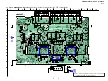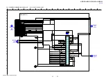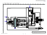
HBD-E2100/E3100/E3200/E4100/E6100
64
• IC Pin Function Descriptions
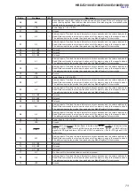
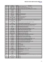
MB1002 BOARD (1/6), (3/6), (4/6) IC101 CXD90019R-BA (BD DECODER)
Pin No.
Pin Name
I/O
Description
P1
TRINB
I
Input of Tracking Signal (B)
P2
TRINA
I
Input of Tracking Signal (A)
P3
HAVC
O
Decoupling Pin for Reference Voltage of Main and Sub Beams
P4
AVDD33_1
-
3.3 V Power Pin
P5
INB
I
Input of Main Beam Signal (B)
P6
INA
I
Input of Main Beam Signal (A)
P7
IND
I
Input of Main Beam Signal (D)
P8
INC
I
Input of Main Beam Signal (C)
P9
ING
I
Input of Main Beam Signal (G)
P10
INH
I
Input of Main Beam Signal (H)
P11
INF
I
Input of Main Beam Signal (F)
P12
INE
I
Input of Main Beam Signal (E)
P13
V14
O
Output of Voltage Reference (1.4 V)
P14
AUX1
I/O
Auxiliary Input
Alternative function: Signal Monitoring
P15
MPXOUT1
O
Multiplexer Output 1 for Signal Monitoring. The pin is not allowed to pull-up in circuit layout.
Alternative function: Internal monitored signal output / General output.
P16
MPXOUT2
O
Multiplexer Output 2 for Signal Monitoring. The pin is not allowed to pull-up in circuit layout.
Alternative function: Internal monitored signal output / General output.
P17
MPXOUT3
O
Multiplexer Output 3 for Signal Monitoring. The pin is not allowed to pull-up in circuit layout.
Alternative function: Internal monitored signal output / General output.
P18
RFIP
I
Differential Input of AC Coupling RF SUM Signal (Positive)
P19
RFIN
I
Differential Input of AC Coupling RF SUM Signal (Negative)
P20
RFIP2
I
Differential Input of AC Coupling RF SUM Signal (Positive)
P21
RFIN2
I
Differential Input of AC Coupling RF SUM Signal (Negative)
P22
AVDD12_2
-
1.2 V Power Pin
P23
AVDD33_3
-
3.3 V Power Pin
P24
FOO
O
Focus servo output. PDM output of focus servo compensator.
P25
TRO
O
Tracking servo output. PDM output of tracking servo compensator.
P26
TLO
O
Tilt servo output
P27
DVCC12_K_1
-
1.2V Digital Power
P28
FEOSCEN
I/O
High frequency modulation enable signal output, or LDD serial interface CLK or I2C SCL.
The pin is spike-free at power-on stage.
P29
FEGAINSW3
O
Read gain switch 3.
P30
FECFREQ
I/O
Frequency selection signal output, or LDD serial interface data or I2C SDA.
The pin is spike-free at power-on stage.
P31
FECMOD
I/O
High frequency modulation mode selection signal output, or LDD serial interface command
enable.
The pin is spike-free at power-on stage.
P32
FEGAINSW1
O
Read gain switch 1.
P33
FEGAINSW2
O
Read gain switch 2.
P34
FEFMO
I/O
Feed motor 4 control. DAC output.
Alternative function: Auxiliary servo input
P35
FEFMO2
O
Feed motor 2 control. DAC output.
P36
DVCC33_IO_1
-
3.3V Digital IO Power
P37
FEFMO3
I/O
Feed motor 3 control. DAC output.
Alternative function: Auxiliary servo input
P38
FEFMO4
I/O
Feed motor 4 control. DAC output.
Alternative function: Auxiliary servo input
P39
FETRAYPWM
O
Tray DAC / PWM control input. Controlled by uP.
P40
FEDMO
O
Disk motor control output. DAC output.
P41
FEFG
I
Motor Hall sensor input.
P42
DVCC12_K_2
-
1.2V Digital Power


