background image

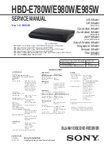
Published by Sony Techno Create Corporation

Sony Corporation

BDV-E780W/E980W/E985W

BLU-RAY DISC/DVD HOME THEATRE SYSTEM

9-893-131-03

2011E05-1

© 

2011.05

US Model
UK Model

BDV-E780W

Canadian Model

Australian Model

BDV-E980W

AEP Model

BDV-E780W/E980W

Saudi Arabia Model

Singapore Model

Taiwan Model

Thai Model

BDV-E985W

Ver. 1.2  2011.05

•  BDV-E780W/E980W/E985W are composed of following models.
  As service manuals are issued for each component model,
  please refer to them.

SPECIFICATIONS

120('202'(/2'2&20321(17(

BDV-E780W

BDV-E980W

BDV-E985W

BLU-RAY DISC/DVD receiver

HBD-E780W

HBD-E980W

HBD-E985W

Front speaker

SS-TSB107

SS-TSB108

SS-TSB108

Center speaker

SS-CTB103

SS-CTB103

SS-CTB103

Surround speaker

SS-TSB106

SS-TSB109

SS-TSB109

Subwoofer

SS-WSB105

SS-WSB105

SS-WSB105

Surround amplifi er

TA-SA300WR

TA-SA300WR

TA-SA300WR

Wireless transceiver

EZW-RT50

EZW-RT50

EZW-RT50

Dock for iPod/iPhone

TDM-iP30

TDM-iP30

TDM-iP30

Note 1:

 As for EZW-RT50 and TDM-iP30, the part number has been described to this service manual.

Note 2:

 TDM-iP30 for BDV-E985W is attached only to Singapore and Thai models.

General

50/60 Hz

5.736 GHz - 5.814 GHz
5.725 GHz - 5.875 GHz

220 V - 240 V AC, 

120 V AC, 50/60 Hz

Power requirements

Power consumption

On: 125 W (BDV-E985W)

Standby: 0.3 W (at the 

On: 130 W 
(BDV-E780W/E980W)

Power Saving mode) 

Dimensions (approx.)

430 mm × 75 mm × 320 
mm (17 in × 3 in × 
12 

5

/

8

 in) (w/h/d) incl. 

projecting parts
430 mm × 75 mm × 333 
mm (17 in × 3 in × 
13 

1

/

8

 in) (w/h/d) (with the 

wireless transceiver 
inserted)

Mass (approx.)

4.1 kg (9 lb 1 oz)

Wireless transceiver (EZW-RT50)

Communication system

Wireless sound 
Specification version 1.0

Frequency band

Modulation method

DSSS

Power requirements

DC 3.3 V, 300 mA

Dimensions (approx.)

30 mm × 9 mm × 60 mm 
(1 

3

/

16

 in × 

3

/

8

 in × 2 

3

/

8

 in) 

(w/h/d)

Mass (approx.)

10 g (

1

/

2

 oz)

Design and specifications are subject to change 
without notice.

s

Standby power consumption 0.3W (main unit), 
0.13W (surround amplifier). 

s

Over 85% power efficiency of amplifier block is 
achieved with the full digital amplifier, S-Master.

Taiwan model:

120 V AC, 60 Hz

US, Canadian models:

s

Standby power consumption 0.3W (main unit), 
0.18W (surround amplifier). 

s

Over 85% power efficiency of amplifier block is 
achieved with the full digital amplifier, S-Master.

Other models:

US, Canadian models:
Other models:

US, Canadian models:

Other models:

s

iPhone, iPod, iPod classic, iPod 
nano, and iPod touch are 
trademarks of Apple Inc., 
registered in the U.S. and other 
countries.

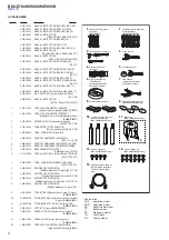
Unpacking

•  Front speakers (2)

•  Surround speakers (2)

•  Center speaker (1)

• Subwoofer  (1)

•  Speaker cords (3, green/gray/blue) (BDV-E780W)

•  Speaker cords (5, red/white/green/gray/blue) (BDV-E980W/E985W)

•  Speaker-bottom covers (4) (BDV-E980W/E985W only)

•  Bases (4) (BDV-E980W/E985W only)

•  Lower parts of the front speakers (4) (BDV-E980W/E985W only)

•  Screws (silver) (4) (BDV-E980W/E985W only)

•  Screws (black) (12) (BDV-E980W/E985W only)

•  FM wire antenna (aerial) (1)

•  Video cord (1)

•  Remote commander (remote) (1)

•  R6 (size AA) batteries (2)

•  Calibration mic (1)

•  High Speed HDMI cable (1) (BDV-E985W only)

•  Dock for iPod/iPhone (TDM-iP30) (1) (Except Saudi Arabian and Taiwan models)

•  USB cable (1) (Except Saudi Arabian and Taiwan models)

• Surround  amplif er (1)

•  Wireless transceivers (4)

• Operating  Instructions

•  Quick Setup Guide

•  Speaker Installation Guide

•  Software Licence Information

•  Easy Setup Disc (DVD) (US, Canadian models only)

•  Wireless Product Compliance Information (AEP, Italian, UK models only)

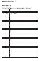
– Refer to next page for accessories list –

MANUAL

 DE SERVIÇO 

Summary of Contents for HBD-E780W

Page 1: ...rsion 1 0 Frequency band Modulation method DSSS Power requirements DC 3 3 V 300 mA Dimensions approx 30 mm 9 mm 60 mm 1 3 16 in 3 8 in 2 3 8 in w h d Mass approx 10 g 1 2 oz Design and specifications are subject to change without notice s Standby power consumption 0 3W main unit 0 13W surround amplifier s Over 85 power efficiency of amplifier block is achieved with the full digital amplifier S Mas...

Page 2: ...OVERALL ASSY Dock for iPod iPhone TDM iP30 EXCEPT EA TW 7 1 835 329 21 CORD CONNECTION USB5P USB cable EXCEPT EA TW 8 1 489 359 11 RF MODULATOR EZW RT50 Wireless transceiver 1 piece AEP IT UK 8 1 489 360 11 RF MODULATOR EZW RT50 Wireless transceiver 1 piece US CND 8 1 489 361 11 RF MODULATOR EZW RT50 Wireless transceiver 1 piece AUS EA SP TH 8 1 489 368 11 RF MODULATOR EZW RT50 Wireless transceive...

Page 3: ...MEMO BDV E780W E980W E985W 3 ...

Page 4: ... allows you to jump to the revised page Also clicking the version at the top of the revised page allows you to jump to the next revised page Ver Date Description of Revision 1 0 2011 03 New 1 1 2011 04 Addition of Italian model 1 2 2011 05 Addition of BDV E985W ...

Page 5: ...o Return Channel OPTICAL Supported formats LPCM 2CH up to 48 kHz Dolby Digital DTS HDMI IN 1 HDMI IN 2 For non European non Saudi Arabia models only Supported formats LPCM 2CH up to 96 kHz Dolby Digital DTS Video Section Outputs VIDEO 1 Vp p 75 ohms COMPONENT Y 1 Vp p 75 ohms PB PR 0 7 Vp p 75 ohms HDMI Section Connector Type A 19pin BD DVD Super Audio CD CD System Signal format system U S and Can...

Page 6: ...xross media bar are trademarks of Sony Corporation and Sony Computer Entertainment Inc PLAYSTATION is a trademark of Sony Computer Entertainment Inc Music and video recognition technology and related data are provided by Gracenote Gracenote is the industry standard in music recognition technology and related content delivery For more information please visit www gracenote com CD DVD Blu ray Disc a...

Page 7: ...B 141 7 12 46 5 16 LDJUDPD VTXHPiWLFR 3ODFD MB 141 8 12 47 5 17 Diagrama Esquemático Placa MB 141 9 12 48 5 18 Diagrama Esquemático Placa MB 141 10 12 49 5 19 Diagrama Esquemático Placa MB 141 11 12 50 5 20 Diagrama Esquemático Placa MB 141 12 12 51 5 21 PODFD GH LUFXLWR PSUHVVR AMP Board DGR ComponentH 52 5 22 PODFD GH LUFXLWR PSUHVVR AMP Board DGR 6ROGD 53 5 23 LDJUDPD VTXHPiWLFR 3ODFD AMP 1 2 5...

Page 8: ...J 2501 305 A HLX 513 Single Layer NTSC J 2501 306 A HLX 514 Dual Layer NTSC J 6090 077 A HLX 506 Single Layer PAL J 6090 078 A HLX 507 Dual Layer PAL TEST DISC Note Refer to the service manual of BDP BX1 S350 Part No 9 883 989 1 page 1 3 to 1 14E for the use of BLX 104 204 Operation and Display 1 BLX 104 Procedure 1 Select 23 976Hz 1080p 2 Play 4 Motion picture 3 Check whether player can play back...

Page 9: ...n by ESD 1 2 Jig Digital camera Recommend with macro mode USB memory PC Barcode decoder Refer to 1 3 Barcode decoder BDPRdec 1 3 Barcode decoder BDPRdec Part No J 6090 212 A Jig name BDPRdec exe Release 2010 11 26 Version 2 0 0 0 Software contents BDPRdec exe Barcode decoder software SavePath ini Decoded f le destination setting f le Ini tial destination is C BuData txt TasmanBars dll Decode dll U...

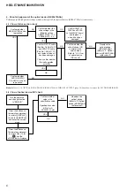
Page 10: ...nd replace it when it has been damaged Confirm whether the optical device IOP is normal in the service mode Refer to 2 2 Flow of optical device IOP check Repalece the optical device KEM 470AAA Refer to 3 Optical device KEM 470AAA replacement NO YES OK YES YES NO NO Note Refer to 2 14 OPTICAL PICK UP BLOCK KEM 470AAA WIRE FLAT TYPE page 19 about how to remove the FFC HOLDER REAR 2 2 Flow of optical...

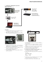
Page 11: ...the taken photo by step 2 to BDPRDec exe and make the text data File name BuData txt 5 Save the text data to USB memory 6 Connect USB memory with rear USB connector on this unit and turn the power on LAN 100 Rear view Rear USB connector 7 Press the FUNCTION button on the remote commander to select BD DVD 8 Press the buttons on the remote commander in order of DISPLAY 0 2 1 SUBTITLE and enter the s...

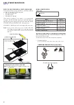
Page 12: ...0 2 W NOTE THE BD DRIVE BPX 6 PARTS REPLACING The mechanism blocks except optical device of BD drive BPX 6 are chief y composed of the following parts CHUCK HOLDER ASSY LOADING ASSY HOLDER FFC REAR These parts are produced by two venders it is not compatible Therefore CHUCK HOLDER ASSY and LOADING ASSY are supplied by one pair as repair parts Please exchange both CHUCK HOLDER ASSY and LOADING ASSY...

Page 13: ...point SSID is displayed on the searching result Note Refer to the instruction manual about details of the setting method 2 Checking method of wired LAN operation Check that access point is recognized surely Procedure 1 Connect the main unit to the router or the hub etc with the LAN cable 2 Press the HOME button on the remote commander to enter the home menu 3 Press the m M buttons on the remote co...

Page 14: ... more SERVICE POSITION 3 tray 1 Remove the left panel E1 Illustration of disassembly is omitted 2 Insert the clip etc tray BD drive Insert the clip etc processed to the length of 8 cm or more in the hole on the side of the chassis and push 8 cm or more hole Side view Top view Note Push after it inserts it in this hole well FL board POWER_SIRCS board MB 141 board AMP board switching regulator SWR1 ...

Page 15: ...K Page 12 2 15 HOW TO BEND FFC Page 20 2 14 OPTICAL PICK UP BLOCK KEM 470AAA WIRE FLAT TYPE Page 19 2 5 FL BOARD Page 13 2 10 WS BOARD Page 15 2 7 WIRELESS LAN CARD WLC1 E780W E980W Page 14 2 12 SWITCHING REGULATOR SWR1 Page 17 2 11 AMP BOARD Page 16 2 9 BD DRIVE BPX 6 Page 15 2 8 TOP LID BLOCK Page 14 2 6 FRONT PANEL BLOCK Page 13 2 3 LOADING PANEL ASSY E1 Page 12 2 13 MB 141 BOARD Page 18 1 scre...

Page 16: ...etc processed to the length of 8 cm or more in the hole on the side of the chassis and push 8 cm or more hole Side view Top view Note Push after it inserts it in this hole well 1 two screws BV3 5 top panel block 2 ten claws 4 connector CN03 1 two screws BV3 3 Lift after doing the slide in the direction of the arrow 5 top panel block 2 ten claws 4 connector CN03 ...

Page 17: ...HBD E780W E980W E985W 13 2 5 FL BOARD 2 6 FRONT PANEL BLOCK 3 two screws BV3 4 FL board 1 wire flat type 19 core CN02 2 connector CN01 1 two screws BV3 2 eight claws 3 front panel block ...

Page 18: ...E780W E980W Note When replacing the wireless LAN card WLC1 refer to CHECKING METHOD OF NETWORK OPERATION page 9 1 two screws BV3 3 harness USB 4 wireless LAN card WLC1 2 3 screw BV3 4 seven screws BV3 5 top lid block 1 wire flat type 19 core CN02 2 connector CN01 Ver 1 2 ...

Page 19: ...ire flat type 45 core CN1301 2 wire flat type 9 core CN2460 3 wire flat type 5 core CN2470 6 Note When you install the BD drive BPX 6 please match the position of the boss two places 8 WS board 4 2 two screws BV3 6 three screws BV3 3 two screws BV3 3 screw BV3 5 slot card WS 7 bracket WS 1 wire flat type 13 core CN55 ...

Page 20: ...or CN451 front side switching regulator SWR1 AMP board Twist wire three times MB 141 board AMP board fan cable LUH VHWWLQJ LUH VHWWLQJ 3 wire flat type 24 core CN3004 5 three screws BV3 8 four screws BV3 9 AMP board 7 screw BV3 6 heat sink S master DDV rear side power insulated lower E1 ...

Page 21: ...r insulated upper E1 power insulated lower E1 harness USB 1 harness USB CN602 front side front side rear side 8 switching regulator SWR1 switching regulator SWR1 switching regulator SWR1 4 power cord connector CN1 5 connector CN101 AMP board 6 connector CN301 LUH VHWWLQJ LUH VHWWLQJ 3RZHU FRUG VHWWLQJ Twist wire three times ...

Page 22: ...N5302 qa connector CN5301 6 fan connector CN6501 C C D D E F G I I G H H qf screw BV3 qg two screws BV3 qg six screws BV3 qd two screws BV3 qd screw BV3 1 four screws BV3 2 drive bracket qh qs three screws B3 u 5 front side WLUH VHWWLQJ MB 141 board AMP board fan cable WLUH VHWWLQJ rear side WLUH VHWWLQJ front side power insulated upper E1 harness USB front side WLUH VHWWLQJ power insulated lower ...

Page 23: ...ype 45 core qj wire flat type 9 core loading assy D qh FFC holder rear 2 two claws 6 8 9 qg 0 3 two claws 4 chuck holder assy D Bottom view 1 wire flat type 45 core Fold Under the guide Under the guide Fold area boss boss loading assy D terminal face terminal face 2 Through the hole 4 Through the hole 3 wire flat type 9 core 5 FFC holder rear 7 two claws 7 three claws 6 QVWDOODWLRQ RI ZLUH IODW W ...

Page 24: ...m 120 mm 35 mm 70 mm MB 141 board CN5907 AMP board CN3004 The upper side is contact side The upper side is contact side MB 141 board CN2460 The upper side is contact side MB 141 board CN1301 MB 141 board CN2470 The upper side is contact side The upper side is contact side The upper side is contact side ZLUH IODW W SH FRUH OHQJWK PP 5HI 1R 11 mm MB 141 board CN5904 WS board CN55 The upper side is c...

Page 25: ...ep 3 press the VOL button on the remote commander and model information is displayed on the f uores cent indicator tube Each time the VOL button on the remote commander is pressed the display changes from destination information STR version in this order and returns to the model informa tion display Each time the VOL button on the remote commander is pressed the version and date are switched 5 In ...

Page 26: ... Diag Performs unit test of devices installed on the board Display Error Log Error log is displayed Displayed contents can also be saved in an USB memory device Factory Initialize Restores the unit to its factory settings Network Checks the wired network connection Version Up Not used System Information Displays the system information of the unit Displays information such as the software version d...

Page 27: ...og Displays Error Log Error Log Displays error log Diag Network Network diagnosis for wired Ping Confirm network connection Ifconfig View network status Device Test US D C IFcon test Video Test Video output test udio Test udio output test udio Input Test udio Input Test ireless L N Test Not used EMC Test Mode Not used Drive Write drive OP data and check drive HDD Mode Not used Start Update for DV ...

Page 28: ... device to test Executes the test M Returns to selection of test category RETURN Returns to selection of test category List of test categories Device Test Video Test Audio Test Audio Input Test Wireless LAN Test not used Mic Test not used HDMI Input Test Transcoder Test not used Diag Category Diag Category Device Test Device Rear USB Media check OK Front USB Media check OK Checking HELP RIGHT UP E...

Page 29: ...st HBD E780W E980W only This screen performs wireless LAN test Note This mode doesn t operate correctly Never use this mode Refer to CHECKING METHOD OF NETWORK OPERATION on page 9 when you conf rm the wireless LAN operation 8 Diag MIC Input Test This screen performs MIC input test Note Not used for the servicing 9 Diag HDMI Input Test This screen performs HDMI input test Screen 1 Select HDMI Input...

Page 30: ...ry de vice errlog log f le is output Select Log HELP DOWN ENT NUM Error Log 08 01 01 00 53 19 ErrCode 080400000000 08 01 01 00 53 45 ErrCode 080400252100 08 01 01 00 54 00 ErrCode 080400005555 1 Error Log Screen 1 Screen 2 12 Factory Initialize Factory Settings There is a possibility that this mode cannot be correctly execut ed Never use this mode 13 Network Network Test Diagnosis Screen Ifconf g ...

Page 31: ... 168 200 13 START HELP ENT Start UP LEFT Ping Ifconfig Ping To START Network Test Ifconfig PING 192 168 200 13 OK Ping 15 System Information System Information Display This screen displays system information Screen 1 Basic Information Operation Drive information delta IOP of a drive is measured and wireless device information displayed go to Screen 2 RETURN Returns to the top menu of the service m...

Page 32: ...rive OP data Write 2 Servo Parameter Check Menu Not used 3 Servo Signal Check Menu Not used 4 S Curve Check Menu Not used 5 Readability Check Menu Not used 6 OP Position Check Menu Not used 7 OP Check Menu Not used 8 Load Eject Aging Not used 9 Spindle Control Check Menu Not used 10 FA Test Mode Not used Screen 2 To start OP data Write Operation Starts Screen 3 Show OP data Write result Operation ...

Page 33: ... the sound output 4 HLX 513 514 NTSC HLX 506 507 PAL Procedure 1 After displayed Main Menu select 1 Video Signal 2 Play 1 Color bar 100 Check the picture and sound output 3 Return to Menu 4 Play Demonstration 4 3 or Demonstration 16 9 Check the picture and sound output 1 2 Playback operation conf rmation Conf rm operation in each signal output mode of test disc BLX 104 204 according to the content...

Page 34: ...Deviation 75 kHz Modulation 1 kHz ANT input 35 dBu EMF Note Please use 75 ohm coaxial cable to connect SG and the set You cannot use video cable for checking Please use SG whose output impedance is 75 ohm 3 Set to FM tuner function and scan the input FM signal with automatic scanning 4 Conf rm that input Frequency of A B and C detected and auto matic scanning stops The stop of automatic scanning m...

Page 35: ...P_DP0 AD2 USB_2P_DM0 AD1 CN602 3 2 VSTB L25 J6001 J501 PB PR Y COMPONENT VIDEO OUT 9 PR OUT 12 PY OUT 10 PB OUT VIDEO AMP IC1003 VIDEO AMP IC6001 PY IN PB IN 4 PR IN MUTE1 5 6 SFDI AG5 LPF SEL 8 MUTE2 7 3 CVBS IN 1 VDACG_OUT VDACB_OUT B19 VDACR_OUT C18 A19 VDACX_OUT C19 14 CVBS OUT VIDEO OUT TXVP_1 B4 COIL MOTOR DRIVER IC2401 XFG 11 MONITOR 12 VSLED1 16 VSLED2 17 SLED1_P 52 SLED1_N 53 SLED2_P 55 S...

Page 36: ... 18 WE NFREN AD4 8 RE NFCEN NFRBN AH2 AE3 9 7 CE RY BY NFALE NFCLE AF4 AG3 17 16 ALE CLE EEPROM IC6601 VDIN31 C21 13 I2C_SDA VDIN30 D21 12 I2C_SCL 4 RESET 19 WP IO1 IO8 X401 27MHz NS_XTALO NS_XTALI B13 A13 CPU_XRST A T2 RESET RRESET AC16 L3 L2 WE M2 BA0 N8 BA1 M3 BA2 CS K3 J3 CAS RAS K9 CKE J7 CK K7 CK D3 C7 DMU DQSU B7 E7 DQSU DML K1 ODT F3 DQSL G3 DQSL L3 L2 WE M2 BA0 N8 BA1 M3 BA2 CS K3 J3 CAS ...

Page 37: ...OWER 18 15 13 RESERVED 14 HDMISO D24 HDMISCK C25 BUFFER Q702 CN701 HDMI ARC OUT B 19 35 D0 _1 D0 _1 45 44 D1 _1 D1 _1 48 47 D2 _1 D2 _1 39 38 CLK _1 CLK _1 B8 A8 RX0 RX0B B7 A7 RX1 RX1B B6 A6 RX2 RX2B B9 A9 RXCK RXCKB 23 22 D0 _SINK D0 _SINK 20 21 D1 _SINK D1 _SINK 17 18 D2 _SINK D2 _SINK 26 27 CLK _SINK CLK _SINK E26 F24 ETRXER DDC_SDA ETTXER DDC_SCL 30 29 SDA_SINK SCL_SINK E27 D28 VDIN0 VDIN1 32...

Page 38: ... GPIO5 AE6 OPWRSB K24 FEGIO3 T6 GPIO6 AE5 GPIO7 AC7 USB_VBUS_PCONT1 SFCS AH5 USB_VBUS_PCONT2 PCONT_FL 27 PCONT_FL PCONT_CORE 38 PCONT_CORE PCONT3 40 PCONT3 PCONT1 PCONT1 82 ATA_PCONT1 43 ATA_PCONT1 E BD_SDO 100 JIG_MODE1 84 ACAL_OUT 68 BD_SDI 1 BD_SCLK 2 BD_CS UPG_STATUS OPWRSB BD_IF_START 21 FE_EJECT BD_IF_REQ 25 88 87 85 86 S AIR_GPIO2 S AIR_DET S AIR_SDA 30 S AIR_RST S AIR_SCL 29 6 90 63 PCONT3...

Page 39: ..._POWER CENTER SUBWOOFER SPEAKERS FRONT R TB451 FRONT L 8 PWM_B OUT_B 6 36 39 31 28 7 PWM_A RESET_AB 5 SD 17 RESET_CD OUT_A D6208 POWER AMP IC3100 14 PWM_C OUT_C PWM_D OUT_D 16 18 INIT 57 DAMP_LATCH3 LAT3 SOFTMUTE OVF1 OVF2 37 DAMP_SHIFT 35 DAMP_SCDT SCSHIFT SCDT LAT1 50 67 DRIVER_SD DRIVER_RST EN AMP_D1 AMP_MCKO AMP_BCKO D AMP_LRCKO D3552 SIGNAL PATH 31 9 11 DATA INIT SOFTMUTE 4 6 48 XFSOIN 38 FSO...

Page 40: ...IC308 A 12V 12V REGULATOR IC5305 A 9V 9V REGULATOR IC5905 CORE 1 1V D 1 8V UNSW 3 3V 1 8V REGULATOR IC3050 1 2VA 1 2V REGULATOR IC304 FRONT USB 5V A 5V 5V REGULATOR IC5908 TUNER 3 3V 3 3V REGULATOR IC104 S AIR 3 3V 3 3V REGULATOR IC50 DCDC 6V DC DC CONVERTER IC5301 OVER VOLTAGE DETECT Q5341 OVER VOLTAGE DETECT Q305 DC DC CONVERTER IC601 REAR USB 5V DC DC CONVERTER IC603 FE_SW 5V 5V REGULATOR IC309...

Page 41: ...ce side Component Side Parts on the pattern face side seen from the pattern face are indicated Parts on the parts face side seen from the parts face are indicated MB 141 board is multi layer printed board However the patterns of intermediate layers have not been included in this diagrams Abbreviation AUS Australian model CND Canadian model EA Saudi Arabia model IT Italian model SP Singapore model ...

Page 42: ... S G E E MB 141 BOARD SIDE A 1 882 505 12 22 P SWR1 SWITCHING REGULATOR M AMP BOARD CN3004 N AMP BOARD CN3003 L FL BOARD CN02 G USB BOARD CN601 F NISECON BOARD CN202 J TUNER BOARD CN101 K WS BOARD CN55 H COMPONENT BOARD CN501 CHASSIS CHASSIS CHASSIS CHASSIS CHASSIS CHASSIS CHASSIS CHASSIS HDMI OUT ARC HDMI IN 1 HDMI IN 2 1 19 18 2 E 1 30 31 50 51 80 81 100 11 1 1 2 23 24 20 11 10 1 1 3 1 2 M1 FAN ...

Page 43: ... JL106 CL5903 C317 R1043 JL2233 C123 JL5307 JL2234 JL5308 JL108 JL109 JL2235 C125 JL5309 C702 C126 JL2236 C127 C129 R6252 JL5310 R6254 JL111 R6255 R746 JL5314 R361 C325 C2401 R749 C131 JL5315 C2402 JL5316 JL116 JL5317 C133 C327 C2404 C1464 JL5318 C328 JL2244 C134 C710 JL2245 C135 C711 C2406 JL2246 C136 C712 JL2247 JL2248 C138 JL505 JL2249 JL312 JL507 JL313 C717 JL508 R6264 JL120 JL509 C719 JL315 C...

Page 44: ...D9998G BB IC101 DVCC15_IO_1 AE10 DVCC15_IO_1 AA11 DVCC15_IO_1 AA13 DVCC15_IO_1 AF13 DVCC15_IO_1 AF14 DVCC15_IO_1 AA15 DVCC15_IO_1 AA17 DVCC15_IO_1 AE17 DVCC15_IO_1 AA19 DVCC15_IO_1 Y20 DVCC15_IO_1 AF20 DVCC15_IO_1 M21 DVCC15_IO_1 P21 DVCC15_IO_1 T21 DVCC15_IO_1 V21 DVCC15_IO_1 R25 DVCC15_IO_1 AA25 DVCC15_IO_1 P26 DVCC15_IO_1 V26 DVCC15_IO_1 AG26 DGND N9 DGND U9 DGND W9 DGND K10 DGND M10 DGND P10 D...

Page 45: ...Y25 RBA0_B AB26 RBA1_B T24 RBA2_B W25 RCKE_B V27 RCS_B_ AB25 RCAS_B_ AC26 RRAS_B_ AD28 RWE_B_ AE28 RODT_B AD27 RRESET_B Y26 K4B1G1646E HCH9 IC206 A0 N3 A1 P7 A2 P3 A3 N2 A4 P8 A5 P2 A6 R8 A7 R2 A8 T8 A9 R3 A10 L7 A11 R7 A12 N7 BA0 M2 BA1 N8 BA2 M3 DMU D3 DQSU C7 DQSU B7 DML E7 DQSL F3 DQSL G3 CK J7 CK K7 CKE K9 CS L2 RAS J3 CAS K3 WE L3 RESET T2 ODT K1 VSS A9 VSS B3 VSS E1 VSS G8 VSS J2 VSS J8 VSS...

Page 46: ...KDZTR3 9B D303 KDZTR3 9B D304 25V C5331 47 16V C5334 100 C5325 10 C5317 10 A12V JL5314 JL5315 JL5316 FL_GND 0 R5352 R5353 1k 1 2 3 3P CN5302 A12V D3 3V DGND 0 R5354 EN_POWER JL5310 1 2 3 4 5 6 7 8 9 10 11 11P CN5301 A 14V UNSW14V FEUNSW14V A GND FE_GND W Surr_GND DGND DGND UNSW6V W Surr_6V EN_POWER W Surr_6V S 1170B33UC OTSTFG IC5302 1 EN 2 VSS 3 NC 4 VIN 5 VOUT 10 C5319 10 C5312 R5344 0 R5345 24k...

Page 47: ...J21 IC101 CXD9998G BB AVDD33_XTAL C15 NS_XTALO B13 NS_XTALI A13 TP_PLLG C14 TN_PLLG D14 AVSS33_XTAL D15 AVDD12_27MPLL E15 AVSS12_27MPLL E14 AVDD12_APLL G15 AVSS12_APLL G14 AVDD12_DMPLL F15 AVSS12_DMPLL F14 AVDD10_LDO K21 AVDD33_LDO J24 AVSS33_LDO H22 R411 0 R509 0 CPU_NFREN CPU_NFALE JL524 JL523 3 3k R523 JL513 R507 0 0 1 C504 RB502 0 JL525 IC101 CXD9998G BB SFCS AH5 SFDI AG5 SFCK AF5 SFDO AH4 NFC...

Page 48: ...20 R606 27k 1 C617 1 C619 D601 DA2J10100L R613 27k R607 10k R614 10k S 1170B50UC OUJTFG IC5601 1 ON OFF 2 VSS 3 NC 4 VIN 5 VOUT BD00GC0WEFJ SE2 IC603 1 VOUT 2 FB 3 GND 4 NC 5 EN 6 NC 7 NC 8 VCC BD00GC0WEFJ SE2 IC601 1 VOUT 2 FB 3 GND 4 NC 5 EN 6 NC 7 NC 8 VCC IC101 CXD9998G BB AVDD12_USB_1P_1 AB3 AVSS12_USB_1P_1 AB6 AVDD12_USB_2P_1A AC4 AVSS12_USB_2P_1A AB5 AVDD33_USB_1P_1 AA3 AVSS33_USB_1P_1 AA6 ...

Page 49: ...D0 _SINK 25 VCC 26 CLK _SINK 27 CLK _SINK 28 GND 29 SCL_SINK 30 SDA_SINK 31 HPD_SINK 32 S1 SCL 33 S2 SDA 34 I2C_SEL 35 HPD1 36 SDA1 37 SCL1 38 CLK _1 39 CLK _1 40 VCC 41 D0 _1 42 D0 _1 43 GND 44 D1 _1 45 D1 _1 46 VCC 47 D2 _1 48 D2 _1 49 LP 50 HPD2 51 SDA2 52 SCL2 53 CLK _2 54 CLK _2 55 VCC 56 D0 _2 57 D0 _2 58 GND 59 D1 _2 60 D1 _2 61 VCC 62 D2 _2 63 D2 _2 64 NC 1k R5799 1k R8701 22 R8702 22 R870...

Page 50: ...LK G24 ETRXCLK G26 ETCRS HPG_RX F26 ETRXD0 F25 ETRXD1 G27 ETRXD2 G28 ETRXD3 G25 ETCOL J27 ETRXDV E25 ETTXER DDC_SCL F24 ETRXER DDC_SDA E26 10V 47 C1001 0 1 C1002 SW5V 0 R6005 560 R1005 GND 0 R6003 JL6002 150 R1008 0 R6007 JL6004 JL6003 JL6001 0 R6015 0 1 C1023 XVMUTE 1 C1025 0 R6006 150 R1007 0 1 C1022 R1035 0 JL6008 5P CN6001 1 PR_OUT 2 GND 3 PB_OUT 4 GND 5 Y_OUT C1012 0 1 1 C1024 0 R6014 BH76071...

Page 51: ... 8 9 10 11 12 13 14 15 16 17 18 19 20 21 22 23 24 24P CN5907 DGND AMP_D3 DGND AMP_D1 DGND AMP_LRCK DGND AMP_BCK DGND AMP_MCK DGND DAMP_LAT3 DAMP_LAT2 DAMP_SCDT DC DET DAMP_LAT1 DAMP_SHIFT DAMP_INIT OVF2 OVF1 SD DAMP_SOFT_MUTE EN SP_OUT FAN 16V 10 C5967 C5974 10 10 C5975 10 C5976 10 C5978 10 C5977 10 C5980 10 C5979 16V 47 C5981 1 C5982 100 R8042 100 R8041 100 R8040 R8043 100 100 R8045 0 R8046 0 R80...

Page 52: ...7 CPU_NFCEN R1105 0 0 R1131 JL1116 JL1115 JL1146 JL1152 JL1148 JL1154 JL1157 JL1156 JL1145 JL1153 JL1155 10k RB1102 R1138 10k R1150 10k XVMUTE JIG_MODE1 R1194 10k ETTXEN R1195 0 3 3VA GND R1146 10k 10k R1144 10k R1143 10k R1142 R1110 10k 5V_RX SDA SCL STRAP_AOSDATA2 STRAP_AOSDATA0 STRAP_AOSDATA1 STRAP_AOLRCK 10k R1161 10k R1162 10k R1163 10k R1165 1 2 3 4 5 6 CN5102 IC101 CXD9998G BB AMUTE D10 VST...

Page 53: ...T8429UL IC6204 1 GND 2 VDD 3 CD 4 OUT 0 01 C6222 10k R6276 1 C6224 1 C6220 0 R6293 R6295 10k 10k R6296 R6298 10k R6200 10k SL6202 R6207 2 7k SL6203 R6302 10k R6303 100k IC6201 R5F3650KBDFA 1 BD_SDI 2 BD_SCLK 3 NO USE 4 SIRCS_IN 5 FL_DOUT 6 S AIR_GPIO2 7 FL_CLK 8 BYTE 9 CNVss 10 ADC_PDN 11 NO USE 12 RESET 13 Xout 14 Vss 15 Xin 16 Vcc 17 CEC TX RX 18 TS_INT 19 KEY_INT 20 AC_CUT 21 BD_IF_START 22 LED...

Page 54: ...1 22 23 24 25 26 27 28 29 30 31 32 33 34 35 36 37 38 39 40 41 42 43 44 45 IC101 CXD9998G BB RFIP K1 RFIN K2 RFIP2 L1 RFIN2 L2 INA G2 INB G1 INC H2 IND H1 INE K3 INF K4 ING J4 INH J3 FECFREQ P5 FECMOD R3 FEOSCEN R5 FOIP C2 FOIN C1 TRINA G3 TRINB H4 TRINC H3 TRIND H5 VRDCO E3 VWDC1O F4 VWDC2O E1 VWDC3O G5 FEMPXOUT1 P2 FEMPXOUT2 N6 FEMPXOUT3 P3 FPDODVD E2 FPDOCD D1 AUX1 G4 FEGAINSW1 T1 FEGAINSW2 P4 F...

Page 55: ...CP2 3 CP1 4 CA5V 5 AGND_1 6 VREF 7 TEST1 8 TEST2 9 TEST3 10 TEST4 11 XFG 12 MONITOR 13 XMUTE1 14 XMUTE2 15 GC 16 VSLED1 17 VSLED2 18 VSPIN 19 VLOAD 20 VTRK 21 VFCS 22 VTLT 23 PGND_1 24 TLT_P 25 TLT_N 26 P5V_1 27 FCS_P 28 FCS_N 29 TRK_P 30 TRK_N 31 P5V12L 32 LOAD_P 33 LOAD_N 34 PGND_2 35 AGND_2 36 TEST5 37 TEST6 38 AGND_3 39 P5V_2 40 C10V 41 P12V_1 42 U 43 ICOM1 44 V 45 P12V_2 46 W 47 ICOM2 48 ISEN...

Page 56: ...33 R3134 C3551 C3552 C3554 Q3551 C3555 Q3552 Q3553 TP3022 TP3026 TP3028 TP3029 D3551 TP3030 TP3031 R3551 TP3032 R3552 R3553 R3554 TP3229 L3051 R3555 TP3036 R3556 L3053 R3557 R3558 R3559 TP3230 TP3231 R3560 CL3001 CL3002 TP3236 CL3003 CL3007 JL3202 JL3210 JL3211 JL3212 JL3213 JL3409 CN3004 C3003 C3201 C3202 C3203 C3204 Q3201 C3205 C3206 C3208 C3209 C3218 C3219 JL3060 C3227 R3203 R3011 R3012 R3207 R...

Page 57: ...015 TP3017 TP3018 TP3019 TP3020 TP3021 L3052 TP3053 TP3054 TP3055 TP3056 TP3057 C3012 C3207 C3013 C3014 C3015 C3016 C3017 C3210 C3020 C3216 C3022 C3217 C3023 C3024 C3025 C3026 C3027 C3220 C3030 C3226 C3051 1 4 1 5 1 4 1 6 C3091 C3099 CN3100 C3111 C3112 C3113 C3114 C3115 C3121 C3122 C3123 C3124 C3125 L3201 L3202 C3553 CN3001 CN3003 CN3200 C3011 C3211 C3212 C3213 C3214 C3215 C3021 C3221 C3222 C3223 ...

Page 58: ...VDD_A NC BST_A GVDD_A RT3CLLM Q3552 3 2 1 4 10uH L3202 EB3002 35V 100 C3122 47 R3231 TP3201 TP3203 JL3213 C3225 2200 35V R3134 47 RT3AMMM Q3202 3 2 1 4 10uH L3101 0 1 C3126 MC2840 T112 1 D3551 JL3110 JL3211 EB3007 SL3001 35V 100 C3211 0 1 C3219 47 R3233 RT3AMMM Q3101 3 2 1 4 10uH L3102 SL3000 TP3104 0 1 C3118 JL3551 47 R3232 SL3002 RT3AMMM Q3201 JL3112 35V 100 C3121 0 1 C3208 C3215 2200 35V C3911 ...

Page 59: ...F FLAGR 25 OVF FLAGL 26 SFLAG 27 INIT 28 MCKSEL 29 LRCK 30 BCK 31 DATA 32 BFVDD 33 BFVSS 34 TEST 35 DVDD 36 XFSIIN 37 FSOCKO 38 FSOI 39 HPOUTR2 40 HPVSSR 41 HPOUTR1 42 HPVDDR 43 HPOUTL2 44 HPVSSL 45 HPOUTL1 46 HPVDDL 47 XVDD 48 XFSOIN CXD9843AR IC3010 1 XVSS 2 VSUBC 3 VSSR 4 OUTR2 5 VDDR 6 OUTR1 7 VSSR 8 VSSL 9 OUTL2 10 VDDL 11 OUTL1 12 VSSL 13 XOVSS 14 XFSOOUT 15 XOVDD 16 DVDD 17 DVSS 18 NSPMUTE ...

Page 60: ...S453 JS454 JS455 JS456 JS457 JS458 CL501 R501 R503 R505 C504 JL501 JL502 JL503 JL504 JL505 JL506 JL507 4 5 1 2 JS501 JS502 JS503 CN501 JW501 J501 CHASSIS S301 A FL BOARD CN01 POWER_SIRCS BOARD 1 883 017 11 11 1 3 CHASSIS USB BOARD 1 883 015 11 11 G MB 141 BOARD CN602 F MB 141 BOARD CN5102 NISECON BOARD 1 883 016 11 11 NC CENTER SUBWOOFER FRONT L FRONT R SPEAKERS CHASSIS CHASSIS D AMP BOARD CN3100 ...

Page 61: ...7 E ET451 C460 0 01 C459 0 01 C458 1000p CL454 CL461 CL452 CL465 CL469 C453 1000p CL459 CL456 C454 1000p CL466 CL457 C456 0 01 C464 0 01 C463 0 01 C455 0 01 CL460 CL455 CL462 C451 0 01 C465 1000p CL458 E ET452 CL453 CL468 CL463 CL451 C452 0 01 C466 1000p 2 3 4 5 6 7 8 9 9P CN451 NC 1 FR FR FL FL SW SW C C JS456 JS452 JS454 JS455 JS457 JS453 JS458 JS451 TB451 75 R503 CL501 75 R505 75 R501 1000p C50...

Page 62: ...32 R33 X10 R49 R56 R57 C11 C13 C14 C17 IC10 IC11 15 C51 C52 C56 C73 CL10 CL11 CL51 CL52 CL53 CL54 CL55 CL56 CL57 CL59 CL60 CL61 CL62 CL63 CL64 CL66 CL67 CL68 CL69 CL70 CL71 CL74 CL78 CL79 CL80 CL81 CL82 CL83 CL84 CL85 CL86 CL87 CL88 CL89 CL93 CL94 R54 R55 R61 R66 R67 R70 C15 C18 C19 C53 C54 C062 C16 WS BOARD COMPONENT SIDE WS BOARD CONDUCTOR SIDE 1 883 019 11 11 1 883 019 11 11 K MB 141 BOARD CN59...

Page 63: ...26 BCK_Y 27 LRCK_Y 28 SDIO_Z 29 BCK_Z 30 LRCK_Z CL53 CL54 CL51 C50 100p CL88 CL89 1 2 3 4 5 6 7 8 9 10 11 12 13 13P CN55 GPIO2 RESET I2C SDA DETECT I2C SCL PCONT1 SD SURR GND BCK GND LRCK WS GND WS 6V CL52 22 R54 18 R55 R53 10 100 R11 100 R56 0 1 C18 100 R12 150 R57 30 29 28 27 26 25 24 7 6 5 4 3 2 1 18 19 20 21 22 23 8 9 10 17 16 11 12 13 14 15 AK4127VF E2 IC11 FILT AVSS PDN SMUTE DITHER PLL2 ILR...

Page 64: ...20 CL21 CL22 CL23 CL24 CL25 CL26 CL27 CL28 CL29 CL30 CL31 CL32 CL33 CL34 CL35 CL36 CL37 CL38 CL39 CL40 CL41 CL42 CL43 CL44 CL45 CL46 CL47 CL48 CL49 CL50 CL51 CL52 CL53 CL54 CL55 CL56 CL57 CL58 CL59 CL60 CL61 CL62 CL63 CL64 CL65 CL66 CL67 R01 R02 R04 R05 R06 R13 R14 R17 R22 R23 R24 R25 R26 R27 R28 R29 R30 R31 JR01 JR04 JR05 JR06 C01 C02 C04 C05 C06 C08 IC01 IC02 IC03 C10 C13 C14 C17 C18 D E E A POW...

Page 65: ... 0 01 CL28 CL01 C01 0 01 MM3404A50URE IC01 1 CE 2 GND 3 Vout 4 Vin MC2837 D03 MC2837 D02 0 022 C10 10k R13 2 7k R06 C20 0 01 D05 DZ2J05100L 0 1 C26 100 R23 100 R24 100 R25 10V 100 C07 35V 47 C15 74AHCT04PW 118 IC03 1 2 3 4 5 6 7 GND 8 9 10 11 12 13 14 Vcc C25 0 1 T01 9 4 6 7 8 2 5 3 1 PT6315 IC02 1 LED1 2 LED2 3 LED3 4 LED4 5 OSC 6 DOUT 7 DIN 8 CLK 9 STB 10 K1 11 K2 12 VSS 13 VDD 14 SG1 15 SG2 16 ...

Page 66: ...37 D101 0 1 C122 100 R118 C123 1 IC101 1 GND 2 VDDRF 3 FRF1 4 FRF2 5 GNDRF 6 CP2 7 NC 8 IIC RDSI 9 LA 10 CK 11 VDD 12 GND 13 DA 14 ROUT 15 LOUT 16 IISD 17 CP1 18 X1 19 X2 20 VDD 100 R120 100k R123 1 2 3 4 5 6 7 7P CN101 R CH A5V L CH AGND I2C_DATA RDS I2C_CLK 100 R124 0 R125 CL105 CL108 CL110 CL111 100 R122 10k R101 FM RECEIVER IC101 3 3V REGULATOR IC104 CHASSIS TUNER BOARD RS5B700 0001E2 US CND A...

Page 67: ...REFERENCE CURRENT LIMIT BIAS IC304 702 MM3404Z11NRE IC307 5301 5307 BD9329AEFJ E2 VOUT 5 NC 4 CE 3 GND 2 VDD 1 VOLTAGE REFERENCE CURRENT LIMIT BIAS VREF OSC IBIAS SLOPE UNDER VOLTAGE LOCK OUT ERROR AMP DRIVE LOGIC S R PWM THERMAL SHUTDOWN LVS LVS OVER CURRENT PROTECT VREG VCC SOFT START BST 1 VIN 2 SW 3 GND 4 EN 7 FB 5 COMP 6 SS 8 ...

Page 68: ... 5 CONT 5 7 8 2 1 3 VOUT FB GND 4 N C VCC N C 6 N C EN SOFT TSD OCP IC705 5908 TK11150CSCL G IC5905 TK11190CSCL G CONTROL CIRCUIT BANDGAP REFERENCE OVER HEAT OVER CURRENT PROTECTION 1 VCONT 3 NP 2 GND 4 VOUT 5 VIN IC1003 BH76071FJ E2 1 CVBS_IN 2 VREF CLAMP REFERENCE 6 75MHz LOW PASS FILTER 3 PY_IN CLAMP 13 5MHz LOW PASS FILTER 30MHz LOW PASS FILTER SD HD 6dB 75 12 PY_OUT 11 GND 13 VCC 4 PB_IN BIAS...

Page 69: ... 4 SWR_SEQ1 8 14 A5V 9 STP2_IN 10 XLEDON 22 REG1PXV 13 XRESET 11 CSWON 19 STP2 21 P5V_SW 17 STP1 18 STP2 20 FB1PXV 15 AGND 16 STP1 12 COLLIENDZ POWER MONITOR LATCH CIRCUIT POWER MOS FET SWITCHING REGULATOR STP1 CONTROL CIRCUIT CURRENT SWITCH CONTROL CIRCUIT SWITCHING REGULATOR VOLTAGE RESET CONTROL STP2 CONTROL CIRCUIT COLLIMATOR END DETECTION PRE DRIVER REFERENCE TSD VCO LED SWITCH LED CONTROL CI...

Page 70: ...ND_2 28 FCS_N 26 P5V_1 32 LOAD_P 34 PGND_2 30 TRK_N 31 P5V12L 33 LOAD_N 29 TRK_P 27 FCS_P ABSOLUTE PWM CONTROL CIRCUIT MATRIX CIRCUIT POWER MOS FET PRE DRIVER PRE DRIVER PRE DRIVER PRE DRIVER POWER MOS FET PRE DRIVER NF NF NF NF NF NF POWER MOS FET PRE DRIVER POWER MOS FET PRE DRIVER POWER MOS FET POWER MOS FET POWER MOS FET ABSOLUTE PWM CONTROL CIRCUIT ABSOLUTE PWM CONTROL CIRCUIT ABSOLUTE PWM CO...

Page 71: ...IN 5 ON OFF 4 1 VSS 2 NC 3 OVERCURRENT PROTECTION THERMAL SHUTDOWN REFERENCE VOLTAGE ON OFF CONTROL 1 VC TSD 2 VIN 3 GND 4 VOUT 5 ADJ REF IC5601 S 1170B50UC OUJTFG 1 ON OFF 2 VSS 3 NC 4 VIN 5 VOUT OVERCURRENT PROTECTOR ON OFF CIRCUIT REFERENCE VOLTAGE CIRCUIT THERMAL SHUTDOWN CIRCUIT ...

Page 72: ... RX 51 SDA2 50 HPD2 D2 _1 47 D2 _1 45 D1 _1 44 D1 _1 42 D0 _1 41 D0 _1 39 CLK _1 38 CLK _1 37 SCL1 36 SDA1 35 HPD1 46 VCC 40 VCC 43 GND TX RX TX RX 34 I2C_SEL 33 32 S2 SDA S1 SCL TX RX RX 31 HPD_SINK 30 SDA_SINK 2 1 MUX LOCAL I2C AND CONTROL LOGIC TX RX 29 SCL_SINK 27 CLK _SINK 28 GND 22 GND 25 VCC TX 26 CLK _SINK TMDS TX 21 D1 _SINK 19 VCC 20 D1 _SINK TMDS TX 18 D2 _SINK 17 D2 _SINK TMDS TX 24 D0...

Page 73: ... B Y 5 Y B GND 4 VCC 8 Y EN G Y IC5906 SN74LV4052APWR 1 2 3 4 5 6 7 8 16 15 14 13 12 11 10 9 2Y0 1Y2 VCC 1Y1 1 COM 1Y0 1Y3 A B GND GND INH 2Y1 2Y3 2 COM 2Y2 IC5907 PCM1808PWR DELTA SIGMA MODULATOR DELTA SIGMA MODULATOR ANTIALIAS LOW PASS FILTER ANTIALIAS LOW PASS FILTER AGND VCC 2 3 VDD DGND 4 5 LRCK 7 REFERENCE u1 64 DECIMATION FILTER WITH HIGH PASS FILTER SERIAL INTERFACE MODE FORMAT CONTROL FMT...

Page 74: ...CLOCK GENERATOR SECONDARY CLOCK GENERATOR PRIMARY 31 29 25 OVFFLAGL 26 SFLAG 27 INIT 30 S g P GAIN CONTROL INIT MUTE SAMPLING RATE CONVERTER FILTER LOW CUT FILTER LINER INTERPOLATOR 6 48 XFSOIN 47 XVDD HPVDDL 46 45 HPOUTL1 HPVSSL 44 43 HPOUTL2 HPVDDR 42 41 HPOUTR1 HPVSSR 40 HPOUTR2 39 37 FSOCKO 38 FSOI 13 XOVSS 14 XFSOOUT 15 XOVDD 16 DVDD 17 DVSS 18 NSPMUTE 19 SOFTMUTE 20 PGMUTE SERIAL CONTROLLER ...

Page 75: ...TORS TO VREG OUT_C BST_C PVDD_C PVDD_D PVDD_D NC BST_D GVDD_D BST_B OUT_B PVDD_B GVDD_A PVDD_A PVDD_A VREG VDD PWM_D RESET_CD PWM_C M1 M2 M3 VREG OC_ADJ PWM_B RESET_AB SD OTW PWM_A 2 NC 3 1 NC GVDD_B 20 NC 19 NC PROTECTION AND I O LOGIC BTL P BTL CONFIGURATION PULLDOWN RESISTORS BTL P BTL CONFIGURATION PULLDOWN RESISTORS BTL P BTL CONFIGURATION PULLDOWN RESISTORS BTL P BTL CONFIGURATION PULLDOWN R...

Page 76: ...ID12 33 SEG19 GRID10 32 SEG18 GRID11 23 SEG10 KS10 24 SEG11 KS11 25 SEG12 KS12 26 SEG13 KS13 22 SEG9 KS9 21 SEG8 KS8 20 SEG7 KS7 19 SEG6 KS6 18 SEG5 KS5 17 SEG4 KS4 16 SEG3 KS3 15 SEG2 KS2 14 SEG1 KS1 MULTIPLEXED DRIVER 34 SEG20 GRID9 35 SEG21 GRID8 36 SEG22 GRID7 37 SEG23 GRID6 39 GRID4 40 GRID3 41 GRID2 42 GRID1 43 VDD 44 VSS 13 VDD 12 VSS 38 SEG24 GRID5 GRID DRIVER WS Board IC11 AK4127VF E2 1 F...

Page 77: ... 0002E2 AEP Italian and UK models 1 FRF1 2 FRF2 3 GNDRF 14 IISD 17 16 X2 X1 18 VDD 19 GND 20 VDDRF 4 CP2 8 CK 7 LA 6 5 IIC RDSI NC 13 LRCK LOUT 9 VDD 10 GND 11 DA FM LNA FILTER FILTER AGC AMP AGC AMP A D CONVERTER D A CONVERTER DIGITAL SIGNAL PROCESSING SERIAL INTERFACE REGISTERS A D CONVERTER CLOCK GENERATOR AGC DET LOSC XSOC 15 CP1 12 BCLK ROUT IC104 MM3404A33URE VOUT 3 CE 1 GND 2 VDD 4 VOLTAGE ...

Page 78: ... the stream processor B13 NS_XTALO I System clock signal input terminal 27 MHz B14 to B16 CH2_P to CH0_P O TMDS data positive output to the HDMI ARC OUT connector B17 CLK_P O TMDS clock positive signal output to the HDMI ARC OUT connector B18 EXT_RES HDMI reference voltage terminal B19 VDACB_OUT O Video PB signal output to the video amplifier US Canadian Australian Singapore Taiwan and Thai models...

Page 79: ...al 1 2V E8 VSS33_HDMI_RX Ground terminal E9 GPIO1 I Ready signal input from the system controller H ready E10 AOSDATA3 O Serial data for audio output output terminal Not used E12 MCIN I Serial data for audio output input from the A D converter E13 SPDIF O SPDIF for digital audio output signal output terminal Not used E14 AVSS12_27MPLL Ground terminal E15 AVDD12_27MPLL Power supply terminal 1 2V E1...

Page 80: ... G25 ETRXD3 I Receive data input terminal Not used G26 ETRXCLK I Receive clock signal input terminal Not used G27 G28 ETRXD1 ETRXD2 I Receive data input terminal Not used H1 IND I Main beam D input from the BD drive H2 INC I Main beam C input from the BD drive H3 TRINC I Tracking signal C input terminal Not used H4 TRINB I Tracking signal B input terminal Not used H5 TRIND I Tracking signal D inpu...

Page 81: ...D Ground terminal L14 DVCC10_K Power supply terminal 1 1V L15 DGND Ground terminal L16 DVCC10_K Power supply terminal 1 1V L17 DGND Ground terminal L18 DVCC10_K Power supply terminal 1 1V L19 DGND Ground terminal L21 DGND Ground terminal L25 VSTB O Video muting on off control signal output to the video amplifier L muting on L26 LCDRD O Serial data output to the system controller L27 RCLK0_B O Cloc...

Page 82: ... interface command enable signal output to the BD drive R4 REIC_MUTE1 O Motor drive muting control signal output to the coil motor driver R5 FEOSCEN O Serial data transfer clock signal output to the BD drive R6 REIC_MUTE2 O Motor drive muting control signal output to the coil motor driver R10 DVCC10_K Power supply terminal 1 1V R11 to R17 DGND Ground terminal R18 DVCC10_K Power supply terminal 1 1...

Page 83: ...minal 1 1V V14 DGND Ground terminal V15 DVCC10_K Power supply terminal 1 1V V16 DGND Ground terminal V17 DVCC10_K Power supply terminal 1 1V V18 DGND Ground terminal V19 DVCC10_K Power supply terminal 1 1V V21 DVCC15_IO_1 Power supply terminal 1 5V V23 V24 RA11_B RA4_B O Address signal output to the SD RAM V25 DGND Ground terminal V26 DVCC15_IO_1 Power supply terminal 1 5V V27 RACK_B O Clock enabl...

Page 84: ...USB_1P_DP I O Two way USB serial data with the USB connector rear side AB3 AVDD12_USB_1P_1 Power supply terminal 1 2V AB5 AVSS12_USB_2P_1A Ground terminal AB6 AVSS12_USB_1P_1 Ground terminal AB11 DGND Ground terminal AB12 RVREF_1 I Reference voltage 0 75V input terminal for SD RAM AB23 AB24 RDQ23_B RDQ21_B I O Two way data bus with the SD RAM AB25 RCS_B O Chip select signal output to the SD RAM AB...

Page 85: ...selection signal output to the NAND flash L busy H ready AE4 NFRBN2 O Ready busy selection signal output terminal Not used AE5 GPIO6 O UPG status signal output to the system controller AE6 GPIO5 O Jig mode selection signal output to the system controller AE7 TMS I Mode selection signal input terminal AE8 AE9 RDQ24 RDQ26 I O Two way data bus with the SD RAM AE10 DVCC15_IO_1 Power supply terminal 1 ...

Page 86: ... AG17 RDQ0 I O Two way data bus with the SD RAM AG19 RDQ9 I O Two way data bus with the SD RAM AG20 RDQS0 O Data strobe signal positive output to the SD RAM AG21 RDQS1_ O Data strobe signal negative output to the SD RAM AG22 RDQ7 I O Two way data bus with the SD RAM AG24 RCLK0 O Clock signal positive output to the SD RAM AG25 RDQ17_B I O Two way data bus with the SD RAM AG26 DVCC15_IO_1 Power supp...

Page 87: ...al 27 PCONT_FL O Power supply on off control signal output terminal for fluorescent indicator tube driver H power on 28 LED_PWM1 O LED drive signal output terminal 29 S AIR_SCL I O Two way I2C clock bus with the wireless transceiver EZW RT50 30 S AIR_SDA I O Two way I2C data bus with the wireless transceiver EZW RT50 31 TXD1 O Not used 32 RXD1 I Not used 33 CLK1 O Not used 34 RTS1 O Not used 35 DA...

Page 88: ... NO USE O Not used 77 TS_SDA I O Two way data bus with the TOUCH board 78 TS_SCL I O Two way clock bus with the TOUCH board 79 ATA_PCONT2 O Power supply control signal output terminal Not used 80 NO USE O Not used 81 SRS_INT O Reset signal output terminal Not used 82 PCONT1 O Power supply on off control signal output terminal H power on 83 BD_RESET O Reset signal output to the BD decoder NAND flas...

Page 89: ...e items The mechanical parts with no reference number in the exploded views are not sup plied Color Indication of Appearance Parts Ex ample KNOB BALANCE WHITE RED Parts Color Cabinet s Color Abbreviation AUS Australian model CND Canadian model EA Saudi Arabia model IT Italian model SP Singapore model TH Thai model TW Taiwan model 6 1 SEÇÃO PANEL The components identified by mark 0 or dotted line w...

Page 90: ...OWER SUPPLY UK EA 0 58 1 837 345 11 CORD POWER SUPPLY TW 59 3 703 244 21 CORD BUSH 2104 EXCEPT TH 59 4 916 783 01 BUSHING CORD TH 60 3 077 331 11 BV3 3 CR WLC1 1 458 327 11 CARD WIRELESS LAN E780W E980W Ref No Part No Description Remark Ref No Part No Description Remark not supplied POWER_SIRCS board not supplied USB board not supplied not supplied not supplied WLC1 back panel section BD drive sec...

Page 91: ...WIRE FLAT TYPE 13 CORE 107 4 256 807 02 CARD SLOT WS M1 1 855 032 11 FAN D C 1 7 682 546 09 SCREW B 3X5 Ref No Part No Description Remark Ref No Part No Description Remark 101 101 102 103 not supplied 1 M1 not supplied NISECON board chassis section not supplied SPEAKER 4P board not supplied not supplied COMPONENT board 101 104 104 104 104 104 104 101 106 101 105 107 not supplied WS board US CND AU...

Page 92: ...COMPLETE for SERVICE E980W CND 9 154 A 1806 891 A MB 141 BOARD COMPLETE for SERVICE E980W AEP IT 9 154 A 1806 892 A MB 141 BOARD COMPLETE for SERVICE E980W AUS 155 1 828 768 51 WIRE FLAT TYPE 24 CORE 156 3 077 331 11 BV3 3 CR 157 A 1795 979 A AMP BOARD COMPLETE 158 4 232 478 31 FOOT 0 SWR1 1 474 270 11 REGULATOR SWITCHING EDPS 170AF B EXCEPT EA 0 SWR1 1 474 271 11 REGULATOR SWITCHING EDPS 170AF C ...

Page 93: ...BLOCK KEM 470AAA C2RP 207 1 838 606 51 WIRE FLAT TYPE 9 CORE 208 1 838 604 51 WIRE FLAT TYPE 45 CORE 209 1 828 292 51 WIRE FLAT TYPE 5 CORE Ref No Part No Description Remark Ref No Part No Description Remark not supplied 202 201 not supplied not supplied 209 208 207 204 206 205 205 205 205 not supplied 203 Note Wires f at type for service is all straight Please bend it referring go HOW TO BEND FFC...

Page 94: ... 10 6 3V C3201 1 100 916 11 CERAMIC CHIP 0 1uF 10 16V C3202 1 100 916 11 CERAMIC CHIP 0 1uF 10 16V C3203 1 165 908 11 CERAMIC CHIP 1uF 10 10V C3204 1 100 916 11 CERAMIC CHIP 0 1uF 10 16V C3205 1 100 916 11 CERAMIC CHIP 0 1uF 10 16V C3206 1 100 916 11 CERAMIC CHIP 0 1uF 10 16V C3207 1 100 597 91 CERAMIC CHIP 0 1uF 10 25V C3208 1 115 339 11 CERAMIC CHIP 0 1uF 10 50V C3209 1 115 339 11 CERAMIC CHIP 0...

Page 95: ...6 805 11 METAL CHIP 47 5 1 10W R3017 1 216 805 11 METAL CHIP 47 5 1 10W R3021 1 218 949 11 METAL CHIP 470 5 1 16W R3022 1 218 949 11 METAL CHIP 470 5 1 16W R3023 1 216 801 11 METAL CHIP 22 5 1 10W R3024 1 216 805 11 METAL CHIP 47 5 1 10W R3027 1 216 805 11 METAL CHIP 47 5 1 10W R3033 1 218 965 11 METAL CHIP 10K 5 1 16W R3040 1 218 990 81 SHORT CHIP 0 R3041 1 218 990 81 SHORT CHIP 0 R3042 1 218 990...

Page 96: ... CHIP 0 1uF 10 16V C27 1 125 837 91 CERAMIC CHIP 1uF 10 6 3V CONNECTOR CN01 1 564 720 11 PIN CONNECTOR SMALL TYPE 4P CN02 1 779 556 21 CONNECTOR FFC LIF NON ZIF 19P CN03 1 564 726 11 PIN CONNECTOR SMALL TYPE 10P DIODE D02 6 501 579 01 DIODE MC2837 D03 6 501 579 01 DIODE MC2837 D05 6 503 014 01 DIODE DZ2J05100L D06 6 502 961 01 DIODE DA2J10100L IC IC01 6 715 344 01 IC MM3404A50URE IC02 6 701 729 01...

Page 97: ... 3V C149 1 114 130 11 CERAMIC CHIP 1uF 10 6 3V C150 1 100 916 11 CERAMIC CHIP 0 1uF 10 16V C152 1 114 130 11 CERAMIC CHIP 1uF 10 6 3V C154 1 114 130 11 CERAMIC CHIP 1uF 10 6 3V C156 1 112 777 11 CERAMIC CHIP 0 01uF 10 25V C157 1 100 916 11 CERAMIC CHIP 0 1uF 10 16V C159 1 112 777 11 CERAMIC CHIP 0 01uF 10 25V C160 1 100 916 11 CERAMIC CHIP 0 1uF 10 16V C170 1 100 909 11 CERAMIC CHIP 10uF 10 6 3V C...

Page 98: ... 0 1uF 10 16V C827 1 100 916 11 CERAMIC CHIP 0 1uF 10 16V C1001 1 128 994 21 ELECT CHIP 47uF 20 10V C1002 1 100 916 11 CERAMIC CHIP 0 1uF 10 16V C1012 1 100 916 11 CERAMIC CHIP 0 1uF 10 16V C1014 1 128 994 21 ELECT CHIP 47uF 20 10V C1017 1 100 966 91 CERAMIC CHIP 10uF 20 10V US CND AUS SP TW TH C1022 1 100 916 11 CERAMIC CHIP 0 1uF 10 16V C1023 1 100 916 11 CERAMIC CHIP 0 1uF 10 16V US CND AUS SP ...

Page 99: ...HIP 220PF 10 50V C5923 1 164 935 11 CERAMIC CHIP 470PF 10 50V C5924 1 137 987 81 CERAMIC CHIP 0 068uF 10 10V C5925 1 125 777 11 CERAMIC CHIP 0 1uF 10 10V C5926 1 164 870 11 CERAMIC CHIP 68PF 5 50V C5928 1 125 891 11 CERAMIC CHIP 0 47uF 10 10V C5930 1 125 777 11 CERAMIC CHIP 0 1uF 10 10V C5935 1 125 777 11 CERAMIC CHIP 0 1uF 10 10V C5938 1 112 298 91 CERAMIC CHIP 1uF 10 16V C5939 1 112 298 91 CERAM...

Page 100: ...16 864 11 SHORT CHIP 0 FB5710 1 400 794 21 EMI FERRITE SMD 1608 FB5902 1 400 827 31 BEAD FERRITE 1005 FILTER FL301 1 234 939 21 FILTER EMI REMOVAL SMD FL302 1 234 939 21 FILTER EMI REMOVAL SMD FL5301 1 234 939 21 FILTER EMI REMOVAL SMD FL5302 1 234 939 21 FILTER EMI REMOVAL SMD FL5701 1 234 939 21 FILTER EMI REMOVAL SMD IC IC101 Not supplied IC CXD9998G BB IC106 6 716 695 01 IC K4B1G1646E HCH9T IC...

Page 101: ...L CHIP 100 5 1 16W R208 1 208 668 11 METAL CHIP 240 0 5 1 16W R209 1 208 668 11 METAL CHIP 240 0 5 1 16W R305 1 218 953 11 METAL CHIP 1K 5 1 16W R307 1 218 953 11 METAL CHIP 1K 5 1 16W R309 1 218 953 11 METAL CHIP 1K 5 1 16W R314 1 216 864 11 SHORT CHIP 0 R327 1 218 953 11 METAL CHIP 1K 5 1 16W R330 1 208 911 11 METAL CHIP 10K 0 5 1 16W R331 1 208 923 11 METAL CHIP 33K 0 5 1 16W R332 1 208 671 11 ...

Page 102: ...16W R1165 1 218 965 11 METAL CHIP 10K 5 1 16W R1169 1 218 965 11 METAL CHIP 10K 5 1 16W R1171 1 218 965 11 METAL CHIP 10K 5 1 16W R1172 1 218 990 81 SHORT CHIP 0 R1173 1 218 990 81 SHORT CHIP 0 R1181 1 216 864 11 SHORT CHIP 0 R1189 1 218 965 11 METAL CHIP 10K 5 1 16W R1194 1 218 965 11 METAL CHIP 10K 5 1 16W R1195 1 218 990 81 SHORT CHIP 0 R1300 1 208 920 81 METAL CHIP 24K 0 5 1 16W R1310 1 218 95...

Page 103: ... METAL CHIP 100 5 1 16W R5908 1 218 957 11 METAL CHIP 2 2K 5 1 16W R5909 1 218 977 11 METAL CHIP 100K 5 1 16W R5910 1 218 969 11 METAL CHIP 22K 5 1 16W R5911 1 218 969 11 METAL CHIP 22K 5 1 16W R5919 1 218 957 11 METAL CHIP 2 2K 5 1 16W R5923 1 218 949 11 METAL CHIP 470 5 1 16W R5927 1 218 933 11 METAL CHIP 22 5 1 16W R5928 1 218 933 11 METAL CHIP 22 5 1 16W R5929 1 218 941 81 METAL CHIP 100 5 1 1...

Page 104: ...7K 5 1 16W R6270 1 218 965 11 METAL CHIP 10K 5 1 16W R6271 1 218 941 81 METAL CHIP 100 5 1 16W R6272 1 218 941 81 METAL CHIP 100 5 1 16W R6274 1 208 721 11 METAL CHIP 39K 0 5 1 16W R6275 1 208 683 11 METAL CHIP 1K 0 5 1 16W R6276 1 208 911 11 METAL CHIP 10K 0 5 1 16W R6277 1 208 699 11 METAL CHIP 4 7K 0 5 1 16W R6278 1 208 911 11 METAL CHIP 10K 0 5 1 16W R6279 1 208 911 11 METAL CHIP 10K 0 5 1 16W...

Page 105: ...5X4 RB502 1 234 400 21 CONDUCTOR NETWORK 1005X4 RB1101 1 234 378 21 RES NETWORK 10K 1005X4 RB1102 1 234 378 21 RES NETWORK 10K 1005X4 RB6201 1 234 372 11 RES NETWORK 100 1005X4 RB6202 1 234 372 11 RES NETWORK 100 1005X4 RB6203 1 234 370 21 RES NETWORK 22 1005X4 RB6204 1 234 372 11 RES NETWORK 100 1005X4 THERMISTOR TH6201 1 804 949 11 THERMISTOR NTC SMD VIBRATOR X401 1 814 278 11 VIBRATOR CRYSTAL 2...

Page 106: ...1 11 PIN CONNECTOR SMALL TYPE 5P CN602 1 822 423 11 CONNECTOR USB A WS BOARD CAPACITOR C11 1 125 837 91 CERAMIC CHIP 1uF 10 6 3V C13 1 162 966 11 CERAMIC CHIP 0 0022uF 10 50V C14 1 162 921 11 CERAMIC CHIP 33PF 5 50V C15 1 107 826 11 CERAMIC CHIP 0 1uF 10 16V C16 1 126 964 11 ELECT 10uF 20 50V C17 1 162 922 11 CERAMIC CHIP 39PF 5 50V C18 1 107 826 11 CERAMIC CHIP 0 1uF 10 16V C19 1 107 826 11 CERAM...

Page 107: ...11 CORD POWER SUPPLY US CND 0 58 1 837 309 21 CORD POWER SUPPLY UK EA 0 58 1 837 345 11 CORD POWER SUPPLY TW 103 1 828 295 51 WIRE FLAT TYPE 7 CORE 105 1 828 286 51 WIRE FLAT TYPE 5 CORE US CND AUS SP TW TH 106 1 828 328 51 WIRE FLAT TYPE 13 CORE 155 1 828 768 51 WIRE FLAT TYPE 24 CORE 202 A 1750 926 A LOADING FOR SERVICE 0 206 8 820 445 04 OPTICAL PICK UP BLOCK KEM 470AAA C2RP 207 1 838 606 51 WI...

Page 108: ... allows you to jump to the revised page Also clicking the version at the top of the revised page allows you to jump to the next revised page Ver Date Description of Revision 1 0 2011 03 New 1 1 2011 04 Addition of Italian model 1 2 2011 05 Addition of HBD E985W ...

Page 109: ...W E880 T58 SS TSB108 is the front speaker in BDV E880 E980 E980W E985W SS WSB104 is the subwoofer in BDV E380 E580 E880 T58 Refer to next page for part list Center SS CTB103 Dimensions approx 315 mm 59 mm 53 mm 12 1 2 in 2 3 8 in 2 1 8 in w h d Mass approx 0 4 kg 15 oz Front Surround SS TSB106 Dimensions approx 96 mm 245 mm 96 mm 3 7 8 in 9 3 4 in 3 7 8 in w h d Mass approx 0 6 kg 1 lb 6 oz Front ...

Page 110: ...nd Rch MX 15 2 893 646 01 FOOT 1 piece Ref No Part No Description Remark 21 A 1798 487 A SS TSB108 Front Lch AEP IT UK 21 A 1798 488 A SS TSB108 Front Lch SP IND 21 A 1798 489 A SS TSB108 Front Lch CND AUS EA TW TH 21 A 1798 490 A SS TSB108 Front Lch MX 21 A 1798 491 A SS TSB108 Front Lch CH 22 A 1798 492 A SS TSB108 Front Rch AEP IT UK 22 A 1798 493 A SS TSB108 Front Rch SP IND 22 A 1798 494 A SS...

Page 111: ...MEMO SS CTB103 TSB106 TSB108 WSB104 3 ...

Page 112: ... 2011 04 Addition of Italian Saudi Arabia Mexican Taiwan Thai and Indian models SS CTB103 Addition of Italian Taiwan and Thai models SS TSB106 Front Addition of Italian Australian Saudi Arabia Mexican Taiwan Thai and Indian models SS TSB106 Surround Addition of Italian Saudi Arabia Mexican Singapore Taiwan and Indian models SS TSB108 Addition of Italian Australian Saudi Arabia Mexican Taiwan Thai ...

Page 113: ...80W E980 E980W E985W Refer to next page for part list Front SS TSB107 Dimensions approx 96 mm 330 mm 72 mm 3 7 8 in 13 in 2 7 8 in w h d wall mounted part 106 mm 325 mm 107 mm 4 1 4 in 12 7 8 in 4 1 4 in w h d whole speaker Mass approx 0 8 kg 1 lb 13 oz wall mounted part 0 8 kg 1 lb 13 oz whole speaker Surround SS TSB109 Dimensions approx 96 mm 775 mm 72 mm 3 7 8 in 30 5 8 in 2 7 8 in w h d wall m...

Page 114: ...A 1798 506 A SS TSB109 Surround Rch CND AUS EA TW TH 12 A 1798 507 A SS TSB109 Surround Rch MX 12 A 1798 508 A SS TSB109 Surround Rch CH 13 A 1801 572 A STAND ASSY TB Lower parts of the front speakers 1 piece Ref No Part No Description Remark 21 A 1795 912 A SS WSB105 Subwoofer AEP IT UK 21 A 1795 913 A SS WSB105 Subwoofer SP IND 21 A 1795 914 A SS WSB105 Subwoofer CND AUS EA TW TH 21 A 1795 915 A...

Page 115: ...SS WSB10 1 Y 8287 765 A BASE MONTADA SS WSB105 ATC Ref No Part No Description Remark VISTA EXPLODIDA 2 Y 8287 763 A GABINETE MONTADO SS WSB105 ATC 1 2 1 ...

Page 116: ...9090 Y 8287 765 A BDV E985W BR BASE MONTADA SS WSB105 ATC Y 8287 719 A 41415 PCI MB 141 MONTADA GRAVADA E985W ATC SBR SPAF 91837 Y 8287 763 A GABINETE MONTADO SS WSB105 ATC 91838 SPAF FORNECEDOR OBS MODELO PN PN ARPC DESCRIÇÃO KLOT não fornecida não fornecida ...

Page 117: ...rsion at the top of the revised page allows you to jump to the next revised page Ver Date Description of Revision 1 0 2011 03 New 1 1 2011 04 Addition of Italian model 1 2 2011 05 Addition of System model name BDV E980 E985W Addition of Chinese Saudi Arabia Mexican Singapore Taiwan Thai and Indian models SS TSB109 WSB105 ...

Reviews: