70
HCD-LF1
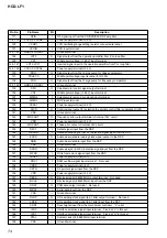
Pin No.
Pin Name
I/O
Description
142
AVDD2
—
Power supply terminal (+3.3V)
143
AVDD1
—
Power supply terminal (+3.3V)
144
AVSS1
—
Ground terminal
145
VDD
—
Power supply terminal (+1.8V)
146
GND
—
Ground terminal
147
XCK
O
Audio system clock output to the A/D converter and digital audio processor
148
LRCK
O
L/R sampling clock signal (44.1 kHz) output to the digital audio processor
149
BCK
O
Bit clock signal (2.8224 MHz) output to the digital audio processor
150
DATA0 (DM)
O
Audio data (for down mix) output terminal
151
DATA1 (FLR)
O
Audio data (for front) output to the digital audio processor
152
VDDP
—
Power supply terminal (+3.3V)
153
GNDP
—
Ground terminal
154
DATA2 (SLR)
O
Audio data (for surround (rear)) output to the digital audio processor
155
DATA3 (CSW)
O
Audio data (for center and sub woofer) output to the digital audio processor
156
IEC958
O
S/PDIF signal output terminal Not used
157
DAI_DATA
I
Data input terminal Not used
158
DAI_BCK
I
Bit clock signal (2.8224 MHz) input terminal Not used
159
DAI_LRCK
I
L/R sampling clock signal (44.1 kHz) input terminal Not used
160
I2C_CL
I/O
Two-way I2C clock bus with the system controller and mechanism controller
161
I2C_DA
I/O
Two-way I2C data bus with the system controller and mechanism controller
162
CS (ZIVA_E2P)
O
Chip select signal output to the EEPROM
163
RXD1
I
Serial data input terminal for check jig
164
TXD1
O
Serial data output terminal for check jig
165
WRITE_CTRL
O
Write control signal output to the EEPROM
(ZIVA_E2P)
166
GNDP
—
Ground terminal
167
VDDP
—
Power supply terminal (+3.3V)
168 to 171 SDDATA7 to SDDATA4
I
Stream data signal input from the DVD decoder
172
GND
—
Ground terminal
173
VDD
—
Power supply terminal (+1.8V)
174 to 177 SDDATA3 to SDDATA0
I
Stream data signal input from the DVD decoder
178
SDREQ
O
Serial data request signal output to the DVD decoder
179
SDEN
I
Serial data enable signal input from the DVD decoder
180
GNDP
—
Ground terminal
181
VDDP
—
Power supply terminal
182
SDERROR
I
Serial data error signal input from the DVD decoder
183
SDCLK
I
Serial data transfer clock signal input from the DVD decoder
184
HIRQ1
I
Interrupt request signal input from the mechanism controller
185
DRVCLK
I
Serial data transfer clock signal input from the mechanism controller
186
DRVTX
I
Serial data input from the EEPROM and mechanism controller
187
DRVRX
O
Serial data output to the EEPROM and mechanism controller
188
DRVRDY
I
Ready signal input from the mechanism controller
189
VNW
—
Power supply terminal (+5V)
190
ALE
O
Latch enable signal output to the address latch
191
RST_SPC
O
Reset signal output to the mechanism controller “L”: reset
192
INT/EXT
O
Internal/external selection signal output terminal
193, 194
HCS2, HCS1
O
Chip select signal output terminal Not used

