82
HCD-LF1
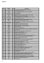
Pin No.
Pin Name
I/O
Description
48
NC
—
Not used
49
NC
—
Not used
50
QUA SI0
O
Touch key scan data output to touch key driver
51
QUA SI1
O
Touch key scan data output to touch key driver
52
QUA SI2
O
Touch key scan data output to touch key driver
53
QUA SO3
I
Touch key data input from touch key driver
54
QUA SO2
I
Touch key data input from touch key driver
55
QUA SO1
I
Touch key data input from touch key driver
56
QUA SO0
I
Touch key data input from touch key driver
57
QUA RST
O
System reset signal output to touch key driver
58
BVDD
—
Power Supply (+5V)
59
BVSS
—
Ground terminal
60
QUA RDY
I
Ready signal input from touch key driver
61
NC
—
Not used
62
NC
—
Not used
63
NC
—
Not used
64
NC
—
Not used
65
NC
—
Not used
66
NC
—
Not used
67
NC
—
Not used
68
NC
—
Not used
69
CDM-CHK-SW
I
Chucking detection switch signal input
70
CDM-OUT-SW
I
Trigger detection switch signal input
71
CDM-TRD-SW
I
Loading out detection switch signal input
72
CDM FIN
O
Motor drive signal output
73
CDM RIN
O
Motor drive signal output
74
AVDD
—
Power Supply (+5V)
75
AVSS
—
Ground terminal
76
AVREF
I
Reference voltage input terminal
77
D.POW SENS
O
Not used
78
NC
—
Not used
79
NC
—
Not used
80
AREA
I
Voltage input terminal of area
81
NC
—
Not used
82
KEY0
I
KEY(power) input terminal
83
KEY1
I
KEY(eject) input terminal
84
KEY2
I
KEY(test mode) input terminal
85
NC
—
Not used
86
NC
—
Not used
87
NC
—
Not used
88
NC
—
Not used
89
NC
—
Not used
90
STOP
I
STOP signal input from Switching Regulator (SA-WSLF1)
91
I/PSW
I
I/PSW signal input from DVD system processor
92
WIDE
I
WIDE signal input from DVD system processor
93
WAKE
O
WAKE output data
94
SIRCS
I
SIRCS signal input from the remote sensor


