background image

2

HCD-LF1H

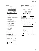
8-5. EMERGENCY HISTORY

To  check the emergency history, please follow the following
procedure.

(1) From the Top Menu of Remocon Diagnosis Menu, select “3.

Emergency History Check” by pressing the  3 “R”  button on
the remote commander. The following screen appears on the
on-screen display.

(2) You can check the total time when the laser is turned on during

playback of DVD and CD from the above menu. The maximum
time, which can be displayed are 9999h 59min.

(3) You can check the error code of latest 10 emergency history

from the above menu. To view the previous or next page of
emergency history, press  

.

 “R”  or  

>

 “R” on the remote

commander. The error code consists of the following three
blocks. The first block indicates the error code. The second
block indicates the parameter and the third block indicates the
time of error code as shown below.

Emg.History Check

1.  01  05  04  04

Laser Hours

CD

9999h

59min

DVD

9999h

59min

00  92  46  00

00  00  00  00

00  00  23  45

2.  02  02  01  01

00  A9  4B  00

00  00  00  00

00  00  23  45


Next   Next Page    Prev  Prev Page

O  Return to Top Menu

8-4-2. EXECUTING IOP MEASUREMENT

In order to execute IOP measurement, the following standard
procedures must be followed.

(1) In power on, press three buttons  

x  

 A  

and  

simultaneously with DVD player.

(2) Select “2. Drive Manual Operation” by pressing the  2 “R”

button on the remote commander. The screen will appear as

     shown.

(3) Select “3. Manual Adjustment” by pressing the  3 “R”  button

on the remote commander. The screen will appear as shown.

(4) Select “6.IOP” by pressing the  6 “R”  button on the remote

commander.

Remocon Diagnosis Menu

0. External Chip Check
1. Servo Parameter Check
2. Drive Manual Operation
3. Emergency History Check
4. Version information

Model Name
IF-con

:  Ver. XX.XX (XXXX)

Syscon

:  Ver. X.XXX

: LFZ5_ XX

*

1

*1: Changes depending on destination 

Drive Manual Operation

1. Servo Control
2. Track/Layer Jump
3. Manual Adjustment
4. Tray Aging Mode
5. MIRR time adjust
0. Return to top Menu

Manual Adjust

1. Track Balance Adjust:
2. Track Gain Adjust:
3. Focus Balance Adjust:
4. Focus Gain Adjust:
5. Eq boost Adjust:
6. Iop:
7. TRV. Level:
8. S curve(FE) Level:
9. RFL(PI) Level:
0. MIRR Time:

o


O

    Change Value

[RETURN] Return to previous menu

TEST MODE

(5) Wait until a hexadecimal number appear.

(6) Convert each data from hexadecimal to decimal using

conversion table.
Use the following formula to calculate IOP in mA.

IOP (mA) = IOP (decimal) 

×

 0.62

(7) Please find the label on the rear of the AUR-M1 (Base Unit).

The default IOP (DVD) value is written in the label.

(8) Subtract between these two values.

(9) If the remainder is smaller than 5mA, then it is OK.

However if the value is higher than 5mA, then the AUR-M1
(Base Unit) is defective and need to be change.

(10) Press the  RETURN “R”  button to return back to previous

 menu.

(11) Press the  0 “R”  button to return to Top Menu and power off

 the DVD Player.

Manual Adjust

1. Track Balance Adjust:
2. Track Gain Adjust:
3. Focus Balance Adjust:
4. Focus Gain Adjust:
5. Eq Boost Adjust:
6. Iop. 5B:
7. TRV. Level:
8. S curve(FE) Level:
9. RFL(PI) Level:
0. MIRR Time:

Change Value
[0] Return to previous menu

Summary of Contents for HCD-LF1H

Page 1: ...Canadian model RU Russian model AUDIO POWER SPECIFICATIONS for the US model POWER OUTPUT AND TOTAL HARMONIC DISTORTION FTC Output Power Front L Front R Center 60 W ch 4 ohms at 170 20 000 Hz 0 7 THD Surround L Surround R 60 W ch 3 5 ohms at 170 20 000 Hz 0 7 THD Subwoofer 110 W ch 1 5 ohms at 40 170 Hz 0 7 THD Super Audio CD DVD system Laser Semiconductor laser Super Audio CD DVD λ 645 660 nm CD λ...

Page 2: ...oint for a slightly longer time Soldering irons using a temperature regulator should be set to about 350 C Caution The printed pattern copper foil may peel away if the heated tip is applied for too long so be careful Strong viscosity Unleaded solder is more viscou s sticky less prone to flow than ordinary solder so use caution not to let solder bridges occur such as on IC pins etc Usable with ordi...

Page 3: ...6 6 Printed Wiring Board DMB14 Board Side B 33 6 7 Schematic Diagram DMB14 Board 1 7 34 6 8 Schematic Diagram DMB14 Board 2 7 35 6 9 Schematic Diagram DMB14 Board 3 7 36 6 10 Schematic Diagram DMB14 Board 4 7 37 6 11 Schematic Diagram DMB14 Board 5 7 38 6 12 Schematic Diagram DMB14 Board 6 7 39 6 13 Schematic Diagram DMB14 Board 7 7 40 6 14 Printed Wiring Board MAIN Board Side A 41 6 15 Printed Wi...

Page 4: ...L SA TSLF1H AC adaptor AC LF1HR Surround speaker R SS TSLF1HW Remote commander RM ADP011 DVD player HCD LF1H Subwoofer SA WSLF1H Front speaker SS TSLF1H Center speaker SS CTLF1H Surround speaker L SA TSLF1H AC adaptor AC LF1HR Surround speaker R SS TSLF1HW 1 Only the defective unit Units with a mark The units that are required for the system operation check during repair service However there can ...

Page 5: ...et on the front part or remove the front part before the repair work front part protective sheet When removing the mech module section AUR M1 create a solder bridge to prevent the optical pick up from breaking Use a soldering iron with an antistatic earth mech module AUR M1 Do not hold the A part of mech module AUR M1 Doing so may deform the module A ...

Page 6: ...s defective disassemble the mech module AUR M1 When re assembling use the new Bottom seal 2 Remove the bottom seal 3 Apply a DC voltage across LDM and LDM on the board DC 2V to 3V 1 Disconnect FFC 50P 160 and them remove the mech module AUR M1 Please refer to SECTION 3 DISASSEMBLY See page 11 for the method removed by the mech module AUR M1 When re assembling use the new Bottom seal DC power suppl...

Page 7: ...7 HCD LF1H SERVICE POSITION MECH MODULE AUR M1 SERVICE POSITION DMB14 BOARD AND MAIN BOARD mech module AUR M1 DMB14 board MAIN board FL board mech module AUR M1 DMB14 board MAIN board FL board ...

Page 8: ...t panel display 115 C 1 standby indicator 42 D DOLBY DIGITAL indicator E DTS indicator F DOLBY PRO LOGIC II indicator G D C S indicator H remote sensor 10 I 1 on standby 42 J Disc slot 42 K Z eject DISC indicator 42 L HDMI OUT jack 36 M Soft touch buttons N x FUNCTION VOLUME 42 When you press the soft touch buttons qd the soft touch indicators 1 light up ...

Page 9: ...rotection compliant device with HDMI or DVI digital visual interface input page 36 SA CD 20 MULTI PBC MUSIC REP1 TRK 28 11 Playing status Current track number Playing time remaining time Current mode Lights up when the MOVIE or MUSIC mode is selected page 47 Lights up when the sleep timer is set page 82 Playing disc Lights up during MULTI channel playback Super Audio CD only page 67 PBC playback V...

Page 10: ...Y THEATRE SYNC 81 Z TV VIDEO 79 wj ENTER1 3 30 44 52 75 84 wk BASS TREBLE 50 wl DVD MENU 59 TOOLS3 79 e DISPLAY 31 52 84 120 TV MENU3 79 ea H play 2 42 54 es x stop 43 54 84 ed X pause 43 ef FUNCTION 2 42 44 75 TV CH 3 79 eg SUBTITLE 66 eh ANGLE 65 ej SA CD CD 67 ek NIGHT 82 el AMP MENU 44 99 124 r TUNER MENU 75 1 The ENTER wj button is the same function as the ENTER 0 button 2 The 5 H and FUNCTIO...

Page 11: ...T 3 2 COVER REAR ASSY HOLDER HDMI Page 12 3 3 LED BOARD Page 13 3 4 TOUCH BOARD Page 14 3 7 BACK PANEL HCD Page 16 3 6 BRACKET SYS A ASSY Page 15 3 8 FL BOARD Page 16 3 12 SHIELD PLATE DMB Page 20 3 5 FRONT SECTION Page 15 3 9 DVD MECHANISM MECH MODULE AUR M1 SECTION 1 Page 17 3 10 DVD MECHANISM MECH MODULE AUR M1 SECTION 2 Page 18 3 11 DVD MECHANISM MECH MODULE AUR M1 SECTION 3 Page 19 3 13 MAIN ...

Page 12: ... screw BVTP 3 6 1 cover screw 3 two claws 4 cover rear assy 5 claw 6 cover HDMI 8 Remove the holder HDMI in the direction of the arrow The front part is easy to be scratched Attach a protective sheet on the front part or remove the front part before the repair work front part protective sheet PRECAUTION THE MAIN UNIT DISASSEMBLY ...

Page 13: ... 3 3 LED BOARD 6 two screws BVTP 2 6 8 7 panel bottom assy 1 connector 10P CN309 3 two claws 2 two screws SS 4 8 connector 10P CN721 5 Remove the saranet cushion 9 three screws BVTP 2 6 8 qa LED board q holder SF ...

Page 14: ... panel top assy 9 five coil springs function 5 Remove the saranet cushion qa connector 13P CN700 6 screw BVTP 2 6 8 7 ground plate function 8 four screws BVTP 2 6 8 qs TOUCH board 2 two screws SS 1 connector 13P CN304 3 two claws 4 ...

Page 15: ...F1H 1 six screws BVTP 3 6 2 front section 1 four screws BVTP 3 6 2 bracket SYS B 6 bracket SYS A assy cable system cable system 5 4 two screws BVTP 3 6 3 screw BVTP 3 6 3 5 FRONT SECTION 3 6 BRACKET SYS A ASSY ...

Page 16: ...16 HCD LF1H 3 four screws BVTP 3 6 1 two screws BVTP 3 6 2 two screws BVTP 3 6 4 back panel HCD 3 FL board 1 four screws BVTP 3 6 2 FFC 7p 100 7core CN951 3 7 BACK PANEL HCD 3 8 FL BOARD ...

Page 17: ...e a soldering iron with an antistatic earth PRECAUTION DVD MECHANISM MECH MODULE AUR M1 DISASSEMBLY 3 FFC 50p 160 50core CN101 2 shield plate CDM 1 two screws BVTP 3 6 4 screw BVTP 3 6 6 two screws BVTP 3 6 5 screw BVTT 3 8 8 two claws qa mech module AUR M1 q two claws 9 7 3 9 DVD MECHANISM MECH MODULE AUR M1 SECTION 1 ...

Page 18: ... five claws 4 2 panel CDM 3 four shafts insulator 5 mech module AUR M1 bracket CDM L etc Do not hold the A part of mech module AUR M1 Doing so may deform the module A 3 10 DVD MECHANISM MECH MODULE AUR M1 SECTION 2 ...

Page 19: ...M ground plate 8 ground plate function 2 two insulators 6 two insulators 4 bracket CDM R 0 bracket CDM L qa mech module AUR M1 3 two screws B EG GRIP 9 two screws B EG GRIP 7 screw BVTP 3 6 3 11 DVD MECHANISM MECH MODULE AUR M1 SECTION 3 ...

Page 20: ...three nylon rivets DIA 3 5 3 shield plate FFC 4 saranet cushion 8 FFC 21p 280 21core CN4502 7 FFC 21p 280 21core CN501 9 three screws BVTP 3 6 q shield plate DMB 6 FFC 15p 280 15core CN4301 5 FFC 15p 280 15core CN601 3 12 SHIELD PLATE DMB ...

Page 21: ...2 connector 10P CN602 4 connector 7P CN502 qf connector 5P CN102 qg saranet cushion two saranet cushions CN102 7 saranet cushion qh MAIN board MAIN board side B qd saranet cushion harness 9 FFC 19p 40 19core CN302 8 FFC 7p 100 7core CN308 6 cable system PRECAUTION DURING HARNESS INSTALLATION Route the harnesses as shown below 3 13 MAIN BOARD ...

Page 22: ...22 HCD LF1H 3 connector 5P CN601 5 DMB14 board 2 six screws BVTP 3 6 1 FFC 19p 40 19core CN109 4 FFC 50p 160 50core CN101 3 14 DMB14 BOARD ...

Page 23: ...ess the VOLUME button 4 To exit from this mode press the 1 button to turn the set off 7 Product Out This mode moves the optical pick up to the position durable to vibration and clears all data including preset data stored in the RAM to initial conditions Use this mode when returning the set to the customer after repair Procedure 1 Press the 1 button to turn the power on 2 Press the FUNCTION button...

Page 24: ...ing on destination Drive Manual Operation 1 Servo Control 2 Track Layer Jump 3 Manual Adjustment 4 Tray Aging Mode 5 MIRR time Adjust 0 Return to Top Menu 8 4 MIRROR TIME ADJUSTMENT To enter Mirror TimeAdjustment press 5 R button on the remote commander The screen will appear as shown There are five main commands in the MIRR time Adjust menu as shown in the figure above The functions of each comma...

Page 25: ...re displayed If it is not same return to step 7 13 Press the A button to eject tray 14 Take out HLX 513 and insert Test Disc HLX A1 into tray 15 Select 1 CD MIRR time check by pressing the 1 R button 16 Wait for HEX number to display 17 Confirm the number if YY is 42 to 79 proceed with next step If no return to step 15 18 Select 4 Save to EEPROM by pressing the 4 R button 19 Confirm the same value...

Page 26: ... to the TEST DISC LIST and press the N button to play the disc back 4 Confirm that oscilloscope waveform is clear and check RF signal level is correct or not Note A clear RF signal waveform means that the shape can be clearly distinguished at the center of the waveform 5 Eject the CD disc and insert the DVD SL test disc refer to the TEST DISC LIST and press the N button to play the disc back Check...

Page 27: ...D PLAY L VIDEO E Y a CHROMA r COMPONENT VIDEO q R G B Abbreviation CND Canadian model RU Russian model For Printed Wiring Boards Note X parts extracted from the component side a Through hole f internal component Pattern from the side which enables seeing The other layers patterns are not indicated Indication of transistor Caution Parts face side Parts on the parts face side seen from SIDE A the pa...

Page 28: ... DVD_SCO 33 100 XIFCS DVD_XIFCS 42 SCO TG_EJ_SW CDM_OPEN 23 SCD SID 98 IFSDO DVD_SOD 32 101 IFSDI 114 XIF5SY 225 SDPIF DVD_XIFBUSY EPM 41 DVD_SID 31 TRO FMOA 1 3 4 FOO DMO TRO FMOB VD1R VD1F 11 12 LDM LDM VD3R VD3F 33 32 36 35 SLED_B SLED_B SLED_A SLED_A 2D2R VD2F VO5R VO5R VO4F 26 SPM_W SPM_V SPM_U W V S VO4R 19 18 21 20 23 22 WIN1 HV WIN2 VIN1 VIN2 UIN1 UIN2 HWN HB HVN 17 TG_EJ_SW HWP HVP HUP HU...

Page 29: ...F1 28 29 VF2 32 33 1 FL DOUT 2 FL CLK 7 FL LAT 22 FL BK 26 LED_DIM 6V Q303 304 LED DRIVER IC101 5V REG D721 DIGITAL 80 DOLBY_LED DST_LED PL_LED DCS_LED Q721 LED DRIVER D722 79 Q722 LED DRIVER DTS D723 78 Q723 LED DRIVER D724 77 Q724 LED DRIVER D C S D725 76 STBY_LED RECT D951 D954 Q951 OSC 6V 6 5 7 RF SECTION Page 28 A TOUCH SECTION Page 31 D RF SECTION Page 28 E DISC_LED BACKLIGHT_LED DISC EJECT ...

Page 30: ...4 73 13 20 11 26 39 38 21 22 24 25 27 31 34 35 40 48 49 51 52 54 55 57 58 22 21 23 32 31 30 63 60 59 24 61 49 50 51 40 41 13 15 14 1 2 4 1 3 6 4 62 2Y 1A 2A 1Y YUV0 MTK RST XRST YUV1 YUV2 YUV3 7 SPDIF ALRCK ABCK ACLK ASDATA1 ASDATA0 ASDATA2 ASDATA4 SMPTE_Y0 SMPTE_Y1 SMPTE_Y2 SMPTE_Y3 SMPTE_Y7 VCLK XTALI SMBSY VSYN 6 5 7 1 2 5 6 1 3 4 6 7 9 10 12 19 15 16 Q701 702 BUFFER IC701 HDMI DRIVER SPDIF ALR...

Page 31: ...INVERTER INVERTER INVERTER INVERTER INVERTER OSC IC756 2 2 D FLIP FLOP CLKB DATAB QB 8 11 12 6 3 2 12 13 2 1 CLKA DATAA QA IC753 1 2 IC753 2 2 KEY 3 KEY 1 10 11 8 9 4 3 6 5 IC754 1 2 D FLIP FLOP IC754 2 2 D FLIP FLOP CLKB DATAB QB 8 11 12 6 3 2 12 13 2 1 CLKA DATAA QA IC751 2 3 IC751 3 3 IC751 1 3 KEY0 10 11 8 9 IC752 D FLIP FLOP CLKB DATAB QB 8 11 12 2 1 4 3 12 13 VOLUME FUNCTION MAIN SECTION Pag...

Page 32: ...R167 R1101 R4322 R191 R1114 R159 R184 R183 R162 R163 R171 R1188 R1161 R166 R164 R1160 R790 R161 R185 R160 R193 R1176 R1179 R1750 R1167 R111 R117 R789 R108 R250 R251 R767 C102 C115 R141 Q103 Q101 R1183 LF704 LF703 LF702 LF701 C190 C187 C148 R152 C197 C180 C177 R230 R247 R260 R231 R153 R137 RB113 R762 RB111 RB103 RB116 RB107 RB110 RB108 RB109 RB112 RB115 RB104 RB117 X101 R520 C1108 C145 C135 C118 R4...

Page 33: ...145 R1150 R148 R146 R754 R110 R151 C220 R756 C215 C730 R190 R197 R248 R1186 R1121 R1102 R1115 R1120 C125 R782 R745 R759 R781 R103 R784 R1149 R143 R1151 R1125 R786 R155 R785 R792 R773 R1710 R760 R703 C198 R1133 R787 R1706 R522 R154 R753 R1201 R765 C524 R112 R158 R138 R105 R556 R1142 R1152 C239 R1141 R1140 R764 R769 C149 C155 R537 R708 R1701 R749 R747 R172 R174 R748 C726 R192 R742 R173 R743 R144 C71...

Page 34: ...01 Q103 Q102 R1133 R151 R116 R111 R108 R117 R114 R1129 R109 R110 R123 R124 R107 IC110 R1178 C183 C198 R1134 C101 C192 C195 C193 R1167 R1168 R142 R1169 IC107 IC105 R1186 R1191 IC109 C1108 C1109 C1111 CL122 CL123 R102 R101 C186 C182 FB101 C153 GND X101 CN103 0 01 0 01 0 01 47 10V 22 22 22 22 22 22 47 4V 15p 0UH 0 01 TC7PAU04FU TE85R 50P 47 10V 47 10V 47 10V 0 1 0 1 0 UM6K1N TN UN2212 TX QST8TR 0 10k...

Page 35: ...1 RB109 RB110 RB113 RB112 IC101 R1192 C1171 C127 C173 R135 C123 C122 C121 R1177 R156 R1201 C162 R126 FB107 C135 C137 C139 C140 C141 C143 C145 C146 C118 R1160 R1161 C161 R1125 R1124 R1123 R1122 R1121 R1120 R1101 JL4703 JL4715 JL4714 JL4713 JL4712 JL4711 JL4710 JL4709 JL4708 JL4707 JL4706 JL4705 JL4704 R4308 R4321 R4701 R4702 R4703 R4704 R4705 R4706 JL4702 JL4701 R4322 R5001 R5002 R5003 CN4301 R136 ...

Page 36: ...1115 JL1116 JL1117 JL1118 JL1119 JL1120 JL1121 JL1122 JL1123 JL1124 JL1125 JL1126 JL1127 JL1128 JL1129 RB108 RB107 RB106 RB105 CN105 IC102 S29AL032D70TF SHE2 0611GA EXCEPT US CND AEP UK 1 0UH 22k 22k 22k 0 0 0 0 0 0 0 0 1 0 1 0 1 0 1 0 1 0UH BR24L64F WE2 EDS6416AHTA 75 E 0 0 10k SN74LVC1G0 8DCKR 0 0 0 19P 10k 10k 1 0k 1 0k 2 7k 47 10V 0 01 47 47 6P 35 35 35 34 35 37 39 34 36 38 43 See page 53 for ...

Page 37: ...R552 R551 R550 R549 R548 R547 C519 C520 C518 C517 C516 C515 C521 C522 C523 C524 R520 R519 C526 C525 R532 R533 R534 FB605 R4801 R4804 R4803 R4802 R4807 R4806 R514 GND 47 10V 47 10V 0UH 0UH 0UH 0UH 0UH 0UH 0UH 0UH AK4358VQ L 0 10 16V 10 16V TK11150CSCL G 0 5P 0UH 47 10V 21P 0 1 0 01 10 220 220 0 47 0 22 0 22 0 47 10V 220 220 0 0 01 0 0 001 220 220 220 220 220 220 220 220 0 01 0 01 0 01 0 01 0 01 0 0...

Page 38: ...18 C217 R229 R225 R217 C224 C223 R216 C222 R215 R214 C205 C206 C207 R259 R260 R261 R241 R240 C215 C230 C220 C211 R230 R231 R232 C216 C221 GND IC203 2SK1828TE85L 0 0 0 0 LMV321IDCKR 0 0 TK11136CSCL G 0 0 0 0 0 0 0 0 0 0 0 0 0 0 0 0 0 0 0 0 47 16V FOO1 TRO1 FOO2 TRO2 FCS TROPENPWM FMOA FMOB DMO1 DMO2 VREFO FG FCS FCS LDM LDM U V W A A B B 0 22 1 0k 4 7k 0 22 0 22 1 0k 33k 18k 15k 82k 680p 680p 5 1k ...

Page 39: ...786 R781 R782 R792 R773 R789 R760 R759 R779 R769 C731 R767 R766 R765 S1701 FL705 R780 R770 R771 R1710 R1715 X701 R1702 R1703 R1701 R764 R790 GND 0 01 0 01 0 01 MB95F108ASPFV GE1 H0601 0 0 2SK1399 T1 B 2SK1399 T1 B 0 0 0 10k 10k 4 7k 100 0 100 0 0 R778 0 0 22 10V 0 4 7k 0 0UH 0 0 0 4 7k 0 10MHz 0 0 0 4 7k 4 7k 6P SLIDE SWITCH EXCEPT AEP UK US CND EXCEPT AEP UK US CND 40 34 35 37 38 40 36 37 35 See ...

Page 40: ...744 R762 R763 R708 R709 R722 R723 R724 R725 R1750 C718 R756 R712 C704 C703 C711 C712 R749 R730 22 10V 10 16V 47 10V 47 4V 0UH 0UH 0UH 0UH SN74LVC1G0 8DCKR 0UH 0UH 0UH 0 0 0 0 0 0 0 0 0 0 0 BR24L16F WE2 CXD9873Q TK11150CSCL G TK11133CSCL G TK11118CSCL G 19P 0 0 01 1 0k 0 22 0 22 1 0k 0 22 0 22 0 1 0 0056 0 1 0 1 0 1 4 7k 10k 4 7k 1 8k 0 01 47k 4 7k 1 0k 0 1 0 22 0 22 0 01 1 0k 0 0 0 0 0 0 0 4 7k 0 ...

Page 41: ...31 C521 C541 C551 C561 C562 C152 C621 C571 C600 C602 C603 C604 C605 C607 C608 C609 C610 C611 C612 C613 C615 C616 C617 C618 C506 CN101 CN102 CN302 CN304 CN301 CN602 CN501 R571 CN601 D301 D501 D502 FB601 FB602 FB603 FB604 FL601 R608 C619 C153 L601 Q301 Q302 Q303 Q304 C601 R301 R302 R306 R307 R308 R309 R310 R311 R313 R315 R317 R359 R316 R318 R326 R327 R328 R331 R332 R333 R334 R335 R339 R358 R350 R354...

Page 42: ... R353 R357 R585 R356 R586 R319 C441 R424 R401 R403 R402 R405 R425 R430 R329 R410 R413 R414 R617 R416 R584 C362 R583 R582 R519 R516 R609 R529 R517 R518 R525 R526 R527 R528 R537 R535 R538 R539 R515 R545 R547 R536 R548 R549 R546 R603 R555 R556 R557 R558 R559 R566 R567 R568 R569 C505 R615 R610 R602 C620 R407 C606 C127 C134 C114 C117 R112 R601 JW601 R305 L132 R394 C394 R393 R395 R397 JW603 R396 R304 L1...

Page 43: ... R332 R333 R334 R328 R327 R326 R325 R323 R322 R321 R320 R319 R318 R317 R316 R353 R352 R315 R314 R343 R313 R312 R311 R310 R309 R308 R305 C302 C301 R351 R350 R306 R303 R302 R301 R393 R413 R416 R414 R412 R411 R410 R409 R408 R396 R397 C395 C394 R395 R394 R407 R406 R405 R404 R403 R402 R401 C311 R378 R379 R375 R374 R354 R447 R446 R445 R444 R443 R442 R441 C442 C441 R346 R357 R338 R337 R329 R376 0 0 1 100...

Page 44: ...84 R583 R582 R581 D501 D502 IC511 C521 C522 C502 C501 C524 C523 C511 C512 C514 C513 IC531 C541 C504 C503 C531 C532 IC551 C506 C505 C551 C561 C542 C552 C562 C533 C543 C563 C553 C534 C544 C554 C564 CN502 IC571 C571 C572 C573 1 21P 2k 2k 1k 1k 4 7k 2k 2k 3 3k 3 3k 1k 4 7k 1k 4 7k 2k 2k 2k 2k 2k 2k 2k 2k 0 3 3k 3 3k 3 3k 3 3k 3 3k 3 3k 3 3k 3 3k 3 3k 3 3k 4 7k 4 7k 4 7k 4 7k 4 7k 1k 1k 1k 1k 1k 4 7k 1...

Page 45: ...601 C606 C601 L601 CN602 C620 Q601 R612 C623 R621 AEP UK RU C621 R617 R615 R602 C605 JW603 C618 C613 R609 C614 C624 R610 C615 C610 C616 C611 C617 C612 C625 R601 CN603 R622 1 50V 1 50V 1 50V 1 50V 1 50V 1 50V 10k 0 0 0 100 6 3V 0UH 0 MM1623BFBE 0 0 0 1 SN74LVC1G125DCKR 0 0 68 68 68 68 68 NJM2870F18 TE2 0 01 15P 0 01 0 01 10P 0 01 RT1N141C TP 1 10k 1 100k 1 0 0 100 100 6 3V 0 470 4V 470 4V 10k 0 01 ...

Page 46: ... D101 D131 IC104 IC102 D111 D121 D141 IC105 IC106 L131 L132 L133 L124 L114 L104 R112 R151 L101 L111 C117 C112 CN101 100 6 3V 100 10V SI 8033S EARTH PLATE EARTH PLATE 10 16V 1000 16V 1000 16V 1000 16V 1000 16V 1000 16V 1000 16V 1000 16V 1000 16V 5P 1 0 01 1 0 1 0 1 0 0 001 0 1 2 2k 0 001 100 0 1 0 1 0 001 0 1 0 SI 8050S LF1101 11EQS04 TB5 10EDB40 TB3 SI 8050S LF1101 11EQS04 TB5 11EQS04 TB5 10EDB40 ...

Page 47: ...956 R971 C956 R951 D958 C970 C960 C966 R954 R955 R956 R957 C962 R967 R968 R953 R965 R960 C953 R959 D957 Q951 R966 R972 R973 R974 R975 C951 C954 C961 C969 FLG901 FLUORESCENT INDICATOR TUBE L951 L952 C952 T951 C955 D951 D953 D954 D955 D952 R952 C973 R981 C971 C972 CN951 R961 1 A B C D E F 2 3 4 5 6 7 8 9 10 Semiconductor Location Ref No Location D951 B 2 D952 B 2 D953 B 2 D954 B 2 D955 D 9 D956 D 9 ...

Page 48: ...N951 Q951 T951 FLG901 C971 C973 R959 R960 C960 C956 C957 C958 C959 R955 R956 R957 R969 R958 R966 R967 R968 R953 R954 R981 C972 MMDL914T1 MMDL914T1 MMDL914T1 MMDL914T1 0 MMDL914T1 MMDL914T1 0 033 200V 47 16V 47 63V MM3Z6V2ST1 22 16V 47 6 3V UDZSTE 173 3B TAR5S33 TE 85R 0 1 680 0 22k 0 1 0 1 100V 0 1 22k 22k 22k 22k 22k 0 1 0 1 100V 7P CPH5504 TL E DC DC CONVERTER FLUORESCENT INDICATOR TUBE 1 1 10 1...

Page 49: ...TP755 SOFT TOUCH BUTTONS TP752 TP753 TP754 TP755 S701 R782 C702 C756 R752 C754 R751 C763 C760 R761 C767 R767 R773 D752 D753 D754 D755 C750 R772 C785 C753 R750 D751 R765 R770 R766 C764 R762 R763 R764 R755 R771 R768 R780 R784 R781 R783 C703 C786 CN721 D721 D722 D723 D724 D725 C732 Q722 C722 C731 R731 1 3 C733 R721 FB731 R722 R724 Q723 R723 C723 R725 C724 Q724 C721 Q721 10 1 A B C D E F G 2 3 4 5 6 7...

Page 50: ...D722 R722 Q722 D723 R723 Q723 D724 R724 Q724 FB731 TP721 TP722 TP723 TP724 TP725 TP726 TP727 TP728 TP729 TP731 TP732 D725 R725 CN721 TP730 IC731 C721 C722 C723 C724 C732 STZ6 8N T146 STZ6 8N T146 STZ6 8N T146 STZ6 8N T146 NSCW100 TE 4 CL 197HB1 D T STZ6 8N T146 22k 13P 0 01 0 01 0 01 220 120 120 1k 1k 1k 1k 1k 0 01 22p 0 1 100k 100 100k 100k 100 100 100k 100k 100 0 1 0 1 100k 0 1 0 1 100k 0 01 0 0...

Page 51: ...601 w CYOUT AEP UK RU models 6 IC601 qk CbOUT AEP UK RU models 6 IC601 qk CbOUT EXCEPT AEP UK RU models 7 IC601 qh CrOUT AEP UK RU models 7 IC601 qh CrOUT EXCEPT AEP UK RU models H 1 3 Vp p H 1 2 Vp p H 1 1 Vp p H 1 2 Vp p H 1 2 Vp p 1 V DIV 100 ns DIV 166 ns 2 6 Vp p 500 mV DIV 20 µs DIV 1 4 Vp p H 500 mV DIV 20 µs DIV 2 2 Vp p H 500 mV DIV 20 µs DIV 2 1 Vp p H H 2 1 Vp p 1 V DIV 20 µs DIV 500 mV...

Page 52: ... 26 V 27 PVcc22 28 RNF2 29 W 30 PGND3 31 VO4F 32 VO4R 33 PVcc3 34 VO5F 35 VO5R 36 Vref 37 CNF5 38 CNF4 39 CNF3 40 CNF2 41 CNF1 42 IN1 43 IN2 44 IN3 45 IN4 46 IN5 47 INSP 48 HB 23 PVcc21 24 Pre Driver Pre Driver NFamp Logic Logic NFamp Pre Driver Pre Driver 180deg MATRIX Pre Driver PH LIMIT T S D OSC OSC REVERSE PROTECT PHASE SHIFT FG 3phase H B Pre Driver Pre Driver Pre Driver NFamp Logic NFamp Lo...

Page 53: ...9 CDTI SDA 20 CSN CAD1 21 DCLK 22 DSDL1 25 DSDR1 26 DSDL2 27 DSDR2 28 DSDL3 29 DSDR3 30 DIF0 31 ROUT4 32 ROUT4 33 VREFH 34 AVDD 35 AVSS 36 LOUT4 37 LOUT4 38 ROUT3 39 ROUT3 40 LOUT3 Audio I F PCM DSD 41 LOUT3 42 ROUT2 43 ROUT2 44 LOUT2 45 LOUT2 46 ROUT1 47 ROUT1 48 DSDL4 23 DSDR4 24 DATT SCF DAC Control Register DATT SCF DAC DATT SCF DAC DATT SCF DAC DATT SCF DAC DATT SCF DAC DATT SCF DAC DATT SCF ...

Page 54: ...CTION HIGHT VOLTAGE GENERATOR 11 bit 8 bit 11 bit STOP START ACK MAIN Board IC101 IC102 SI 8050S LF1101 OVER CURRENT PROTECTOR LATCH DRIVER OVER HEAT PROTECTOR REGULATOR RESET VREF COMPARATOR ERROR AMP OSC 1 VIN 2 SW OUT 3 GND 4 VOS 5 S S IC103 SI 8033S OVER CURRENT PROTECTOR LATCH DRIVER OVER HEAT PROTECTOR REGULATOR ON OFF SOFT START RESET VREF COMPARATOR ERROR AMP OSC 1 VIN 2 SW OUT 3 GND 4 VOS...

Page 55: ...5MHz 75Ω DRIVER LOW PASS FILTER 6 75MHz 75Ω DRIVER 20 CY OUT 75Ω DRIVER S DC OUT S1 S2 26 C OUT LOW PASS FILTER 6 75MHz 75Ω DRIVER CLAMP 150kΩ BIAS LOW PASS FILTER 6 75MHz LOW PASS FILTER 13 5MHz 18 CB OUT 19 GND2 17 GND2 15 GND2 75Ω DRIVER LOW PASS FILTER 6 75MHz LOW PASS FILTER 13 5MHz 14 CR IN 150kΩ BIAS 16 CR OUT 75Ω DRIVER LOW PASS FILTER 6 75MHz LOW PASS FILTER 13 5MHz 6dB 6dB IC603 NJM2870F...

Page 56: ...18 TNI I 3 beam satellite PD signal negative input 19 TPI I 3 beam satellite PD signal positive input 20 MDI1 I Laser power monitor input 21 MDI2 I Laser power monitor input 22 LDO2 O Laser driver output 23 LDO1 O Laser driver output 24 SVDD3 Power supply RF 3 3V 25 CSO O Central servo positive main beam summing output not used 26 RFLVL O RFRP low pass or Positive main beam summing output not used...

Page 57: ... ROM IC102 85 DVSS Ground terminal 86 to 88 HD 4 to 6 I Data bus 4 to 6 input from FLASH ROM IC102 89 HA21 O Address bus 21 output to FLASH ROM IC102 90 ALE O Address latch enable not used 91 HD7 I Data bus 7 input from FLASH ROM IC102 92 HA17 O Address bus 17 output to FLASH ROM IC102 93 HA0 O Address bus 0 output to FLASH ROM IC102 94 DVSS Ground terminal 95 UWR I System controller write strobe ...

Page 58: ...d terminal 145 BA1 O BA1 signal output to SD RAM IC104 146 RA10 O Address bus 10 output to SD RAM IC104 147 RA0 O Address bus 0 output to SD RAM IC104 148 DVSS Ground terminal 149 to 151 RA 1 to 3 O Address bus 1 to 3 output to SD RAM IC104 152 DVDD18 Power supply 1 8V from IC110 153 RVREF Reference voltage not used 154 RCLKB Dram clock not used 155 DVDD3 Power supply SW 3 3V 156 DRCLK O CLK signa...

Page 59: ...V5 O CB B signal output to VIDEO AMP IC601 203 YUV6 O CR R signal output to VIDEO AMP IC601 204 DVDD3 Power supply SW 3 3V 205 VSYN O Active low vertical sync output to HDMI Driver IC701 206 YUV7 O Main audio mute signal not used 207 SMBSY O Active low horizontal sync output to HDMI Driver IC701 208 SMSCK O SMS clock output 209 SMSDI I Audio data of SPDIF input 210 SMSDO O SMS data output 211 XSMC...

Page 60: ... supply RF 3 3V 240 VCM I Not used 241 VSS Ground terminal 242 VREFP I SACD top reference 243 VREFN I SACD bottom reference 244 RFVDD3 Power supply RF 3 3V 245 RFRPDC I RFRP signal input 246 RFRPAC I RFRP signal input 247 HRFZC I High frequency RF ripple zero crossing 248 CRTPLP O Defect level filter capacitor connecting 249 RFGND Ground terminal 250 CEQP Not used 251 CEQN Not used 252 OSP I RF of...

Page 61: ... 26 LED_DIM O LED 6V control signal output 27 NC Not used 28 BACKLIGHT_LED O KEY BACKLIGHT LED control signal output 29 I2C_CLK I O I2C CLOCK Pull up 30 I2C_DATA I O I2C DATA Pull up 31 DVD_SID O MEDIA TEK data out 32 DVD_SOD I MEDIA TEK data in 33 DVD_SCO I MEDIA TEK clock in 34 SYS_BUSY I SIO BUSY control signal input from System controller SA WSLF1H 35 SYS_RXD O Serial data output to System con...

Page 62: ...C Not used 74 POWER_KEY I POWER KEY input 75 NC Not used 76 STBY_LED O STANDBY LED drive signal output 77 DCS_LED O DCS LED drive signal output 78 PL_LED O PROLGIC LED drive signal output 79 DTS_LED O DTS LED drive signal output 80 DOLBY_LED O DOLBY DIGITAL LED drive signal output 81 to 95 NC Not used 96 AVss Ground terminal 97 NC Not used 98 Vref Power supply BUP 3 3V 99 AVcc Power supply BUP 3 3...

Page 63: ...74 079 01 COVER SS 3 2 674 060 01 COVER SCREW 4 X 2109 469 1 PANEL TOP ASSY 5 4 238 532 11 SCREW SS 6 2 674 056 01 SPRING FUNCTION COIL 7 3 831 441 99 CUSHION 8 A 1181 591 A TOUCH BOARD COMPLETE 9 3 087 053 01 BVTP2 6 3CR 10 2 674 053 01 PLATE FUNCTION GROUND 11 A 1181 589 A LED BOARD COMPLETE 12 2 674 036 01 HOLDER SF 13 X 2109 470 1 PANEL BOTTOM ASSY 14 2 674 025 01 COVER HDMI 15 2 674 026 01 HO...

Page 64: ... SHAFT PMMA 52 2 674 018 01 PANEL PMMA EXCEPT AEP UK RU 52 2 674 018 11 PANEL PMMA AEP UK RU 53 2 674 038 01 PANEL AL HCD US CND 53 2 674 038 21 PANEL AL HCD EXCEPT US CND 54 2 177 732 01 SPRING B LEAF 55 7 684 023 04 N 3 TYPE 2 56 2 674 019 01 WINDOW FL 57 X 2148 674 1 HOLDER WINDOW ASSY 58 7 688 004 01 W 4 SMALL 59 2 674 080 01 SHEET FL INSULATING US Ver 1 1 ...

Page 65: ...ETE EA3 9 102 A 1199 893 A DMB14 BOARD COMPLETE AUS 9 102 A 1199 894 A DMB14 BOARD COMPLETE MX 9 102 A 1199 896 A DMB14 BOARD COMPLETE KR 9 102 A 1199 897 A DMB14 BOARD COMPLETE TW 9 102 A 1199 898 A DMB14 BOARD COMPLETE HK 9 102 A 1199 900 A DMB14 BOARD COMPLETE CH 9 102 A 1217 891 A DMB14 BOARD COMPLETE E41 103 1 828 355 51 WIRE FLAT TYPE 19 CORE 104 A 1181 582 A MAIN BOARD COMPLETE EXCEPT AEP U...

Page 66: ... 155 156 152 153 153 152 153 152 153 154 151 2 674 371 01 PANEL CDM 152 2 674 078 01 SHAFT INSULATOR 153 2 634 618 01 INSULATOR 154 4 672 834 01 SCREW B EG GRIP 0155 8 342 200 00 MECH MODULE AUR M1 US CND AEP UK 0155 8 342 200 11 MECH MODULE AUR M1 11 EXCEPT US CND AEP UK 156 2 694 437 01 SEAL BOTTOM US CND AEP UK 157 2 674 053 01 PLATE FUNCTION GROUND 2 7 685 645 79 SCREW BVTP 3X6 TYPE2 IT 3 Ver ...

Page 67: ... CHIP 1uF 10 10V C123 1 165 908 11 CERAMIC CHIP 1uF 10 10V C124 1 165 908 11 CERAMIC CHIP 1uF 10 10V C125 1 107 826 11 CERAMIC CHIP 0 1uF 10 16V C126 1 107 826 11 CERAMIC CHIP 0 1uF 10 16V C127 1 162 970 11 CERAMIC CHIP 0 01uF 10 25V C128 1 162 965 11 CERAMIC CHIP 0 0015uF 10 50V C129 1 165 989 11 CERAMIC CHIP 10uF 10 6 3V C130 1 107 826 11 CERAMIC CHIP 0 1uF 10 16V C131 1 125 889 91 CERAMIC CHIP ...

Page 68: ...519 1 162 970 11 CERAMIC CHIP 0 01uF 10 25V C520 1 162 970 11 CERAMIC CHIP 0 01uF 10 25V C521 1 162 970 11 CERAMIC CHIP 0 01uF 10 25V C522 1 162 970 11 CERAMIC CHIP 0 01uF 10 25V C523 1 162 970 11 CERAMIC CHIP 0 01uF 10 25V C524 1 162 970 11 CERAMIC CHIP 0 01uF 10 25V C525 1 162 970 11 CERAMIC CHIP 0 01uF 10 25V C526 1 162 970 11 CERAMIC CHIP 0 01uF 10 25V C527 1 127 715 91 CERAMIC CHIP 0 22uF 10 ...

Page 69: ...CL G IC703 6 702 302 01 IC TK11133CSCL G IC705 6 703 046 01 IC SN74LVC1G08DCKR IC706 not supplied IC BR24L16F WE2 IC707 6 705 337 01 IC TK11150CSCL G IC708 6 806 298 01 IC MB95F108ASPFV GE1 H0601 LINE FILTER LF701 1 813 308 11 COMMON MODE CHOKE LF702 1 813 308 11 COMMON MODE CHOKE LF703 1 813 308 11 COMMON MODE CHOKE LF704 1 813 308 11 COMMON MODE CHOKE TRANSISTOR Q101 6 550 008 01 TRANSISTOR UM6K...

Page 70: ...216 821 11 METAL CHIP 1K 5 1 10W R231 1 216 821 11 METAL CHIP 1K 5 1 10W R232 1 216 821 11 METAL CHIP 1K 5 1 10W R233 1 216 864 11 SHORT CHIP 0 R234 1 216 864 11 SHORT CHIP 0 R235 1 216 864 11 SHORT CHIP 0 R236 1 216 864 11 SHORT CHIP 0 R237 1 216 864 11 SHORT CHIP 0 R238 1 216 864 11 SHORT CHIP 0 R239 1 216 864 11 SHORT CHIP 0 R240 1 216 815 11 METAL CHIP 330 5 1 10W R241 1 216 810 11 METAL CHIP ...

Page 71: ...ERRITE EMI SMD 1608 R1129 1 216 845 11 METAL CHIP 100K 5 1 10W R1133 1 216 864 11 SHORT CHIP 0 R1134 1 216 864 11 SHORT CHIP 0 R1138 1 216 864 11 SHORT CHIP 0 R1139 1 216 864 11 SHORT CHIP 0 R1140 1 216 864 11 SHORT CHIP 0 R1141 1 216 864 11 SHORT CHIP 0 R1142 1 216 864 11 SHORT CHIP 0 R1143 1 216 864 11 SHORT CHIP 0 R1145 1 216 295 91 SHORT CHIP 0 R1146 1 216 864 11 SHORT CHIP 0 R1149 1 216 864 1...

Page 72: ... 16V C971 1 109 982 11 CERAMIC CHIP 1uF 10 10V C972 1 162 970 11 CERAMIC CHIP 0 01uF 10 25V C973 1 109 982 11 CERAMIC CHIP 1uF 10 10V CONNECTOR CN951 1 784 366 51 CONNECTOR FFC FPC 7P DIODE D951 8 719 081 97 DIODE MMDL914T1 D952 8 719 081 97 DIODE MMDL914T1 D953 8 719 081 97 DIODE MMDL914T1 D954 8 719 081 97 DIODE MMDL914T1 D955 8 719 056 82 DIODE UDZ TE 17 6 2B D956 8 719 081 97 DIODE MMDL914T1 D...

Page 73: ... 10 25V C154 1 109 982 11 CERAMIC CHIP 1uF 10 10V C301 1 107 826 11 CERAMIC CHIP 0 1uF 10 16V C302 1 107 826 11 CERAMIC CHIP 0 1uF 10 16V C304 1 107 826 11 CERAMIC CHIP 0 1uF 10 16V C305 1 107 826 11 CERAMIC CHIP 0 1uF 10 16V C306 1 107 826 11 CERAMIC CHIP 0 1uF 10 16V C309 1 126 206 11 ELECT CHIP 100uF 20 6 3V C311 1 107 826 11 CERAMIC CHIP 0 1uF 10 16V C351 1 107 826 11 CERAMIC CHIP 0 1uF 10 16V...

Page 74: ...8 719 085 36 DIODE 11EQS04 TB5 D121 8 719 085 36 DIODE 11EQS04 TB5 D131 6 500 522 21 DIODE 10EDB40 TB3 D141 6 500 522 21 DIODE 10EDB40 TB3 D301 8 719 081 97 DIODE MMDL914T1 D501 6 501 193 01 DIODE 1SS355WTE 17 D502 6 501 193 01 DIODE 1SS355WTE 17 EARTH TERMINAL EP101 1 537 738 21 TERMINAL GROUND EP102 1 537 738 21 TERMINAL GROUND EP301 1 537 738 21 TERMINAL GROUND EP302 1 537 738 21 TERMINAL GROUN...

Page 75: ...10W R340 1 216 809 11 METAL CHIP 100 5 1 10W R341 1 216 809 11 METAL CHIP 100 5 1 10W R342 1 216 833 11 METAL CHIP 10K 5 1 10W R343 1 216 833 11 METAL CHIP 10K 5 1 10W R344 1 216 809 11 METAL CHIP 100 5 1 10W R345 1 216 833 11 METAL CHIP 10K 5 1 10W R346 1 216 864 11 SHORT CHIP 0 R350 1 216 864 11 SHORT CHIP 0 R351 1 216 833 11 METAL CHIP 10K 5 1 10W R352 1 216 829 11 METAL CHIP 4 7K 5 1 10W R353 ...

Page 76: ...61 1 218 271 11 METAL CHIP 2K 5 1 10W R562 1 218 271 11 METAL CHIP 2K 5 1 10W R563 1 216 827 11 METAL CHIP 3 3K 5 1 10W R564 1 216 827 11 METAL CHIP 3 3K 5 1 10W R565 1 216 829 11 METAL CHIP 4 7K 5 1 10W R566 1 216 821 11 METAL CHIP 1K 5 1 10W R567 1 216 821 11 METAL CHIP 1K 5 1 10W R568 1 216 829 11 METAL CHIP 4 7K 5 1 10W R569 1 216 825 11 METAL CHIP 2 2K 5 1 10W R571 1 216 864 11 SHORT CHIP 0 R...

Page 77: ...11 METAL CHIP 22K 5 1 10W R765 1 216 809 11 METAL CHIP 100 5 1 10W R766 1 216 809 11 METAL CHIP 100 5 1 10W R767 1 216 809 11 METAL CHIP 100 5 1 10W R768 1 216 809 11 METAL CHIP 100 5 1 10W R770 1 216 845 11 METAL CHIP 100K 5 1 10W R771 1 216 845 11 METAL CHIP 100K 5 1 10W R772 1 216 845 11 METAL CHIP 100K 5 1 10W R773 1 216 845 11 METAL CHIP 100K 5 1 10W R774 1 216 845 11 METAL CHIP 100K 5 1 10W ...

Page 78: ...78 HCD LF1H MEMO ...
Page 79: ...d EMERGENCY HISTORY of the TEST MODE of DVD SECTION The TEST MODE of the DVD SECTION contains the following tests For all the information other than what are described in this SUPPLEMENT 1 refer to the original SERVICE MANUAL 9 887 283 0 TEST MODE DVD SECTION 8 Mirror Time Check 8 1 GENERAL DESCRIPTION 8 2 HOW TO ENTER TEST MODE 8 3 DRIVE MANUAL OPERATION 8 4 MIRROR TIME ADJUSTMENT 8 4 1 EXECUTING...

Page 80: ...g the 3 R button on the remote commander The screen will appear as shown 4 Select 6 IOP by pressing the 6 R button on the remote commander Remocon Diagnosis Menu 0 External Chip Check 1 Servo Parameter Check 2 Drive Manual Operation 3 Emergency History Check 4 Version information Model Name IF con Ver XX XX XXXX Syscon Ver X XXX LFZ5_ XX 1 1 Changes depending on destination Drive Manual Operation ...
Page 81: ...turn to Top Menu 1 2 3 8 5 2 Clear the Emergency History Press TOP MENU R button and then press CLEAR R button The error code for all emergency history would be reset Emg History Check 1 01 05 04 04 Laser Hours CD 0h 0min DVD 0h 0min 00 92 46 00 00 00 00 00 00 00 23 45 2 02 02 01 01 00 A9 4B 00 00 00 00 00 00 00 23 45 Next Next Page Prev Prev Page O Return to Top Menu Emg History Check 1 00 00 00 ...

Page 82: ... Revision 1 0 2006 07 New 1 1 2006 09 Addition of Korean Taiwan Mexican Russian Singapore Saudi Arabia Hong Kong E41 230 V AC area in E model and Australian models The components identified by mark is added SPM 06046 SUPPLEMENT 1 EXECUTING IOP MEASUREMENT and EMERGENCY HISTORY for TEST MODE ENG 06007 1 2 2006 10 Addition of Chinese model 1 3 2006 12 Change of TEST DISC LIST of electrical adjustmen...

Reviews: