HCD-SLK1i/SLK2i
59
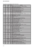
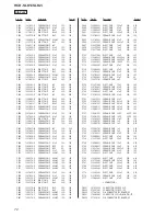
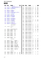
Pin No.
Pin Name
I/O
Description
165
LCD SCL(SPI)
O
Serial data transfer clock signal output to the liquid crystal display module
166
LCD DCLK
O
Data clock signal output to the liquid crystal display module
167
LCD HSYNC
O
Horizontal sync signal output to the liquid crystal display module
166
LCD DE
O
Data enable signal output to the liquid crystal display module
169
LCD VSYNC
O
Vertical sync signal output to the liquid crystal display module
170
LCD CS(SPI)
O
Chip select signal output to the liquid crystal display module
171
LCD SDA(SPI)
I/O
Two-way data bus with the liquid crystal display module
172
DVSS
-
Ground terminal
173
LCD GBR
O
GBR signal output to the liquid crystal display module
174
iPod LINE MUTE
O
Not used
175
SD/MS INS
I
SD memory card and memory stick insert detection signal input terminal
176
SD WP
I
SD memory card write protect detection signal input terminal
177
SD CARD DET
I
SD memory card detection signal input terminal
178
DAC SMUTE
O
Muting on/off control signal output to the audio D/A converter “H” muting on
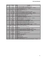
179
VDD3.3
-
Power supply terminal (+3.3V)
180
SD CMD/MS BS
O
Command signal (for SD memory card) and bus state signal (for memory stick) output
terminal
181
SD/MS CLK
O
Serial data transfer clock signal (for SD memory card and memory stick) output terminal
182
iPod CP RESET
O
Reset signal output to the EEPROM “L”: reset
183, 184
SD/MS DAT3,
SD/MS DAT2
I/O
Two-way data (for SD memory card and memory stick) bus terminal
185
VDD1.2
-
Power supply terminal (+1.2V)
186, 187
SD/MS DAT1,
SD/MS DAT0
I/O
Two-way data (for SD memory card and memory stick) bus terminal
188
SELB
O
Video signal selection signal output terminal
189
DVSS
-
Ground terminal
190
SELA
O
Video signal selection signal output terminal
191
Video AMP A MUTE
O
Muting on/off control signal (for DVD VIDEO OUT jack) output to the video ampli
fi
er
“L”: muting on
192
Video AMP B MUTE
O
Muting on/off control signal (for liquid crystal display module) output to the video ampli
fi
er
“L”: muting on
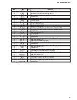
193
Video Dec RESET
O
Reset signal output to the video A/D converter “L”: reset
194
Video Dec AVID
I
Active video indicator signal input from the video A/D converter
195
Video Dec
INTREQ/GPCL
I
Interrupt request and general purpose control signal input from the video A/D converter
196
Video Dec PDN
O
Power down signal output to the video A/D converter “L”: power down
197
AML BUSY
O
Busy signal output to the system controller
198
VDD3.3
-
Power supply terminal (+3.3V)
199
Video Dec PCLK
I
Pixel clock signal input from the video A/D converter
200
Video Dec VSYNC
I
Vertical sync signal input from the video A/D converter
201
Video Dec HSYNC
I
Horizontal sync signal input from the video A/D converter
202
Video Dec AVID
I
Field indicator and color PLL information signal input from the video A/D converter
203
UART Rx
I
Serial data input from the system controller
204
UART Tx
O
Serial data output to the system controller
205
I2C SDA
I/O
Two-way I2C data bus with the EEPROM and video A/D converter
206
I2C SCK
O
I2C clock signal output to the EEPROM and video A/D converter
207
VDD3.3
-
Power supply terminal (+3.3V)
208
VSS3.3
-
Ground terminal
209
OSCIN
I
System clock input terminal (24MHz)
210
OSCOUT
O
System clock output terminal (24MHz)
211
MCLK
O
Master clock signal output to the audio A/D converter
212
BCK
O
Bit clock signal output to the audio A/D converter
213
LRCK
O
L/R sampling clock signal output to the audio A/D converter
214
MDATA
O
Digital audio data output to the audio A/D converter
215
CARD VCC ENABLE
O
Power on/off control signal output terminal for SD memory card and memory stick
“H”: power on
216
RESET
I
Reset signal input from the system controller “L”: reset
216
RESET
I
Reset signal input from the system controller “L”: reset

