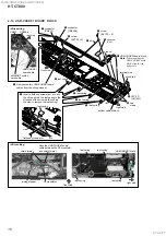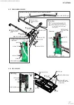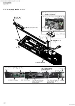
background image

HT-CT800

22

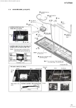
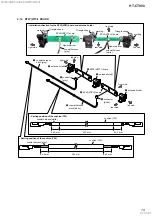
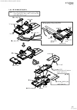
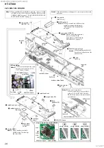
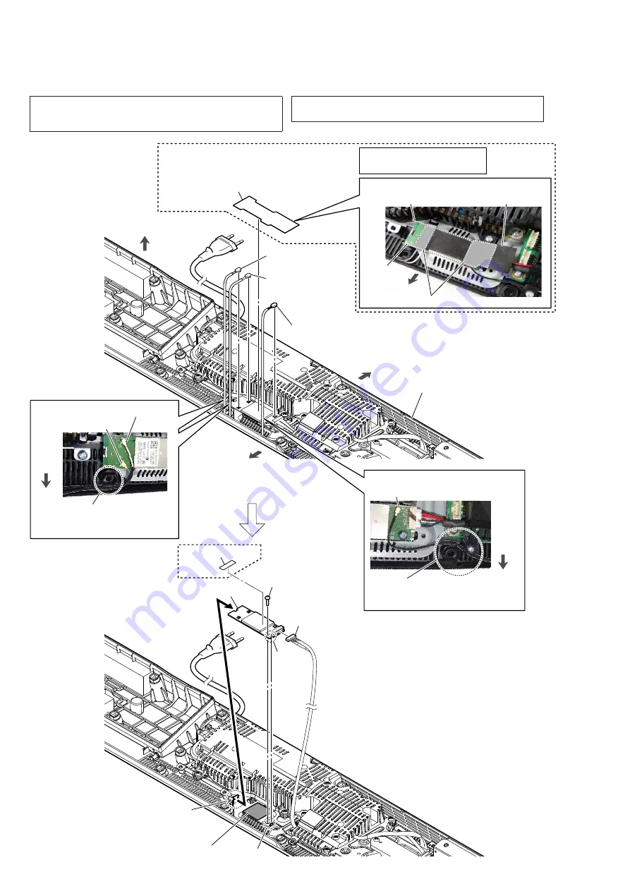
2-17.  WLAN/BT  COMBO  CARD (WIFI1)

XXX XX: X-XXXXX

             X-XXX-XXX-XX

1

 cushion (WIFI label)

bottom cabinet block

2

 connector (No. 

3

)

 [gray]

2

 connector (No. 

2

)

 [white]

[white]: No. 

2

Pass the coaxial harness 
across the front side of 
the screw hole.

[gray]: No. 

3

[black]: No. 

1

Pass the coaxial harness 
across the rear side of 
the screw hole.

‡:LUHVHWWLQJ

‡:LUHVHWWLQJ

2

 connector (No. 

1

)

 [black]

rear side

top side

front 
side

front side

front side

3

 screw

 (BVTP3 

u

 8)

6

 CNC label (AR2)

5

 MB-1612 board 

 cable 

connector

4

 claw

rib

groove

7

 WLAN/BT combo card (WIFI1)

 Note 

4:

 When installing the WLAN/BT combo card,  


align the rib and groove.

radiation sheet

‡3DVWLQJSRVLWLRQRIWKHFXVKLRQ:,),ODEHO

guide line

guide line

Pressing the adhesive area.

cushion (WIFI label)

front side

Note 3:

 This part is deleted from 


the midway of production.

$5

Note 1: 

When the WLAN/BT combo card (Ref. No. WIFI1) is re-
placed, refer to “NOTE OF REPLACING THE MB-1612 
BOARD OR WLAN/BT COMBO CARD” on page 5.

Note 2: 

If the radiation sheet is damaged, be sure to replace them with 
new parts.

Ver. 1.3

SYS SET

2019/09/24 22:06:08 (GMT+09:00)

Summary of Contents for HT-CT800

Page 1: ... SP1 AR TH AUS CH CH 3 Codec Audio signal compression and conversion format 4 Abbreviation for Subband Codec 5 Abbreviation for Advanced Audio Coding CH BLUETOOTH section Communication system BLUETOOTH Specification version 4 1 Output BLUETOOTH Specification Power Class 1 Maximum communication range Line of sight approx 30 m1 Maximum number of devices to be registered 9 devices Frequency band 2 4 ...

Page 2: ...y Corporation WALKMAN and WALKMAN logo are registered trademarks of Sony Corporation PlayStation is a registered trademark or trademark of Sony Interactive Entertainment Inc MPEG Layer 3 audio coding technology and patents licensed from Fraunhofer IIS and Thomson Windows Media is either a registered trademark or trademark of Microsoft Corporation in the United States and or other countries This pr...

Page 3: ... Side B 30 TABLE OF CONTENTS 3 TEST MODE 31 4 TROUBLESHOOTING 40 5 DIAGRAMS 5 1 Block Diagram HDMI Section 44 5 2 Block Diagram MAIN Section 45 5 3 Block Diagram AMP Section 46 5 4 Block Diagram PANEL POWER SUPPLY Section 47 5 5 Printed Wiring Board MB 1612 Board 49 5 6 Printed Wiring Board USB CHUKEI Board 50 5 7 Schematic Diagram USB CHUKEI Board 50 5 8 Printed Wiring Boards ANTENNA Section 51 5...

Page 4: ...15 AEP UK SP1 AR TH LA AUS CH 800 2 W 800 2 W 800 2 W NOTE OF PERFORMING THE OPERATION CHECK IN THE STATE THAT HEAT SINK IS REMOVED When performing the operation check in the state that this unit is disassembled it is possible to perform the operation check in the state that heat sink is removed However don t perform the opera tion check in the long time and perform the operation check in the volu...

Page 5: ...P2P address to Registry 8 Press the button on the remote commander wait until the display show Status Write Successful refer to Screen 2 9 Press the BACK button on the remote commander to return to category select screen and press the b button on the re mote commander to select Bluetooth Device Test refer to Screen 3 10 Press the button on the remote commander to select 1 Bluetooth Enable 11 Press...

Page 6: ...ss the V v buttons on the remote commander to select the Internet Settings and press the button on the remote commander 8 Press the V v buttons on the remote commander to select the Wired Setup and press the button on the remote commander 9 Press the V v buttons on the remote commander to select the Auto and press the b button on the remote command er 10 The The network will be configured with the...

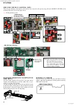
Page 7: ...he MB 1612 board is not described NOTE OF REPLACING THE ELECTRICAL PARTS ON EACH BOARDS FOR REPAIRING Among mounted electrical parts on each boards only parts that are described in the electrical parts list can be replaced for repair The parts that are not described in the electrical parts list cannot be replaced with single for repairing WIRELESS CONNECTION LINK WORK OF BAR SPEAK ER AND SUBWOOFER...

Page 8: ... the bond to be used for other parts Also a contact surface refer to left figure of the CONTACT TERMINAL be careful absolutely bond does not adhere MALFUNCTION PREVENTION OF THE BUTTON TOUCH PANEL SWITCH When the button portion on the top side of the main unit are touched with something such as the floor surface there is a pos sibility of occurring the malfunction When performing the operation che...

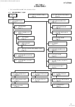
Page 9: ... 14 2 9 LOUDSPEAKER L CH SP1 Page 15 2 5 SIRCS BOARD Page 12 2 6 DISPLAY BOARD Page 12 2 7 ORGANIC EL INDICATOR ELEMENT OLED1 Page 13 2 12 NFC BOARD Page 17 2 17 WLAN BT COMBO CARD WIFI1 Page 22 2 18 INSULATION TOP ASSY Page 23 2 10 USB CHUKEI BOARD BLOCK Page 16 2 11 USB CHUKEI BOARD Page 17 2 13 BTW WIFI BOARD BLOCK Page 18 2 15 BTW BT BOARD BLOCK Page 20 2 14 BTW WIFI BOARD Page 19 2 16 BTW BT ...

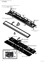
Page 10: ...e right side 1 twelve screws BVTP3 u 8 3 FFC 18P CN5003 terminal side 2 Open the top cabinet block in the direction of the arrow right side rear side 6 top cabinet block top side Note 2 Take care not to crush the front grille 5 R ch speaker cable connector CN6003 4 L ch speaker cable connector CN6002 guide line top cabinet block top side L ch speaker cable R ch speaker cable rear side 6SHDNHU FDEO...

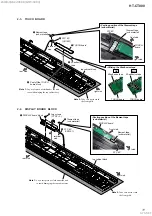
Page 11: ...h under the unit to avoid damaging the top cabinet assy 3DVWLQJ SRVLWLRQ RI WKH ILODPHQW WDSH VXE PDWHULDO IIL LQJ WKH DGKHVLYH WDSH front side OK NG right side 2 two screws PTP2 u 5 rear side right side top cabinet block 3 5 DISPLAY board block DISPLAY board Note 1 Lay a soft piece of cloth under the unit to avoid damaging the top cabinet assy Note 2 Take care not to crush the front grille termin...

Page 12: ...lock boss boss hole groove 3 two screws PTP2 u 5 9 FFC 18P CN1303 1 connector CN891 hook 2 Remove the wire from the hook 4 Open the DISPLAY board block in the direction of the arrow 8 connector CN1304 terminal side 0 DISPLAY board Note When installing the DISPLAY board align the groove and hole with the two bosses 5 Unlock CN1302 Bend the wire hook SIRCS board bottom side terminal side 6 Insert a ...

Page 13: ...NDICATOR ELEMENT OLED1 top side right side left side DISPLAY bracket block 2 Peel the organic EL indicator element off of the adhesive sheet 3 organic EL indicator element OLED1 1 cushion OLED SYS SET 2019 09 24 22 06 08 GMT 09 00 ...

Page 14: ...the two grooves QVWDOODWLRQ GLUHFWLRQ ZKHQ FRQQHFWLQJ WKH WHUPLQDOV RI WKH FRQQHFWLRQ FDEOH 5 FK QVWDOODWLRQ GLUHFWLRQ IRU WKH ORXGVSHDNHU 5 FK 63 Note 1 Lay a soft piece of cloth under the unit to avoid damaging the top cabinet assy rear side rear side right side right side QVWDOODWLRQ SRVLWLRQ RI WKH SDFNLQJ RQQHFWLRQ FDEOH 5 FK VHWWLQJ 5 screw BVTP3 5 5 screw BVTP3 5 top cabinet block groove gr...

Page 15: ...eft side 1 tape 1 two tapes QVWDOODWLRQ SRVLWLRQ RI WKH SDFNLQJ RQQHFWLRQ FDEOH FK VHWWLQJ groove packing CL3 packing CL3 gray black loudspeaker L ch SP1 left side tape two tapes Press front side Note 2 Take care not to crush the front grille loudspeaker L ch SP1 wide narrow QVWDOODWLRQ GLUHFWLRQ IRU WKH ORXGVSHDNHU FK 63 rear side left side OK NG OK NG Note 3 When connecting the terminals of the ...

Page 16: ...spring leaf spring USB CHUKEI board 7 connector CN501 8 connector CN5004 bottom cabinet block rib 2 Insert a flathead screwdriver etc into the slit and slide the leaf spring in the direction of the arrow while pushing the claw to remove the leaf spring qa USB CHUKEI board block Note When installing the USB CHUKEI board block align the rib and groove wiring stopper Pass the USB CHUKEI board cable b...

Page 17: ...e cable along the white line on the USB CHUKEI board Note 2 When affixing the cushion CZ2 A be careful that it does not obstruct the screw hole USB CHUKEI board USB CHUKEI board screw hole 1 mm to MB 1612 board to USB CHUKEI board 5HDU YLHZ guide line cushion CZ2 A MB 1612 board connection cable 6P 5 MB 1612 board connection cable 6P front side right side 2 FFC 6P CN001 terminal side bottom cabine...

Page 18: ... the adhesive area cushion WIFI label RD LDO KDUQHVV ZKLWH JUD VHWWLQJ front side left side BTW WIFI 1 board white No 2 Pass the coaxial harness across the front side of the screw hole gray No 3 BTW WIFI 2 board slot slot front side Pass the coaxial harness across the front side of the screw hole Pass the coaxial harness across the front side of the screw hole Note This part is deleted from the mi...

Page 19: ... block gray 3 coaxial harness block white 2 connector gray 2 connector white coaxial harness gray coaxial harness white 1 antenna holder 1 antenna holder 1 antenna holder 4 BTW WIFI 2 board 4 BTW WIFI 1 board top side left side right side 3DVWLQJ SRVLWLRQ RI WKH FXVKLRQ 7 coaxial harness gray coaxial harness white cushion T03 cushion T03 3DVWLQJ SRVLWLRQ RI WKH FXVKLRQ 7 BTW WIFI 1 board BTW WIFI ...

Page 20: ...s the rear side of the screw hole Pass the coaxial harness across the front side of the screw hole slit rib rib rib front side right side 3DVWLQJ SRVLWLRQ RI WKH FXVKLRQ ODEHO guide line guide line Pressing the adhesive area cushion WIFI label slot BTW BT board front side Pass the coaxial harness across the rear side of the screw hole Note This part is deleted from the midway of production Ver 1 3...

Page 21: ...gle shape coaxial harness black 2 connector black 1 antenna holder 4 BTW BT board 1 antenna holder Triangle shape marking marking 3DVWLQJ SRVLWLRQ RI WKH FXVKLRQ 7 coaxial harness black cushion T03 top side left side right side 3 coaxial harness block black to BTW BT board to WLAN BT combo card rear side front side SYS SET 2019 09 24 22 06 08 GMT 09 00 ...

Page 22: ... BVTP3 u 8 6 CNC label AR2 5 MB 1612 board cable connector 4 claw rib groove 7 WLAN BT combo card WIFI1 Note 4 When installing the WLAN BT combo card align the rib and groove radiation sheet 3DVWLQJ SRVLWLRQ RI WKH FXVKLRQ ODEHO guide line guide line Pressing the adhesive area cushion WIFI label front side Note 3 This part is deleted from the midway of production 5 Note 1 When the WLAN BT combo ca...

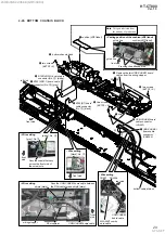
Page 23: ...w 3 Draw out the power cord block from the hole 6 power cord AC1 5 cord bushing FBS001 4 Unlock power cord AC1 cord bushing FBS001 lock side 85 0 5 mm to POWER board lock side white US CND blue Except US CND power cord cord bushing FBS001 front side left side bottom cabinet block QVWDOODWLRQ SRVLWLRQ RI WKH FRUG EXVKLQJ 6 Note When installing the power cord block check the direction and position o...

Page 24: ...SING on page 4 3 screw BVTP3 u 8 rib rib hole hole rear side white US CND blue Except US CND power cord screw hole LUH VHWWLQJ POWER board guide line C6050 C977 C6068 C976 front side Note 3 The wire must not touch the screw boss and four capacitors C976 C977 C6050 C6068 MB 1612 board screw boss 3 two screws BVTP3 u 8 front side right side bottom cabinet block 1 cushion WS label 3 screw BVTP3 u 8 2...

Page 25: ...9 RF modulator RF1 Note 2 When installing the RF modulator align the rib and groove RF modulator block front side bottom side 3DVWLQJ SRVLWLRQ RI WKH FXVKLRQ starting point center guide line RF modulator block top side front side cushion CL3 5 Note 1 When the RF modulator RF1 is replaced refer to WIRE LESS CONNECTION LINK WORK OF BAR SPEAKER AND SUBWOOFER on page 7 Ver 1 3 SYS SET 2019 09 24 22 06...

Page 26: ... terminal side front side rear side top side bottom cabinet block LUH VHWWLQJ slot C6024 Pass the cable between the C6024 and L6006 L6006 AMP heat sink WLAN BT combo card cable LJ USB CHUKEI board cable wiring stopper Pass the USB CHUKEI board cable between the RF modulator and shield main shield main RF modulator Pressing the adhesive area guide line overlap 1 mm cushion CL3 guide line cushion WS...

Page 27: ...four screws BVTP3 u 8 1 screw BVTP3 u 8 1 screw BVTP3 u 8 1 screw BVTP3 u 8 1 screw BVTP3 u 8 1 two screws BVTP3 u 8 2 ground plate 3 shield main block bottom cabinet block front side rear side top side SYS SET 2019 09 24 22 06 08 GMT 09 00 ...

Page 28: ...the shield HDMI align the three legs and three holes shield HDMI shield HDMI shield HDMI shield HDMI clip clip clip clip 4 AMP heat sink Note 3 When you install the AMP heat sink spread the compound referring to SPREADING OF COMPOUND on page 8 3 two screws BVTP3 u 8 1 connector CN6001 Note 6 Before connect this connector refer to CAPACITOR ELECTRICAL DISCHARGE PROCESSING on page 4 LUH VHWWLQJ RZ W...

Page 29: ...8 front side left side bottom cabinet block front side LUH VHWWLQJ 3DVWLQJ SRVLWLRQ RI WKH FXVKLRQ ODEHO guide line guide line Pressing the adhesive area cushion WIFI label white No 2 Pass the coaxial harness across the front side of the screw hole gray No 3 black No 1 LUH VHWWLQJ LUH VHWWLQJ front side USB CHUKEI board cable wiring stopper Pass the USB CHUKEI board cable between the RF modulator ...

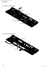
Page 30: ...800 30 2 27 SERVICE POSITION SIDE A 2 28 SERVICE POSITION SIDE B MB 1612 board POWER board insulating sheet RF modulator block MB 1612 board POWER board insulating sheet SYS SET 2019 09 24 22 06 08 GMT 09 00 ...

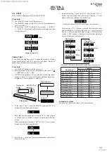
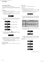
Page 31: ...ken into account When touching the all buttons OK and K 6 are alternately displayed on the front panel display K 6 OK 5 Press the 2 button on the remote commander and return to the state of step 3 6 In the state of step 3 touch the VOL button and CG3_A model name is displayed on the front panel display A will display differs depending on the destination CG3_A Displayed characters in the above figu...

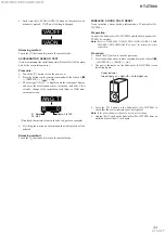
Page 32: ...nd check whether there is no space between the TOUCH board and the top cabinet Releasing method Press the 1 button on the remote commander and return to the normal mode AMP TEST It can perform the AMP setting and measurement Procedure 1 Touch the 1 button to turn the power on 2 Press the buttons on the remote commander in the order of x DISPLAY 2 V 3 The message MSURE is displayed on the front pan...

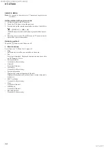
Page 33: ...nformation that is displayed will be updated Releasing method Touch the 1 button and return to the normal mode WIRELESS SOUND COLD RESET It can initialize various backup information of Subwoofer SA WCT800 Preparation Connect the Subwoofer SA WCT800 and the Bar Speaker SA CT800 by wireless Note Refer to WIRELESS CONNECTION LINK WORK OF BAR SPEAKER AND SUBWOOFER on page 7 for details of wireless con...

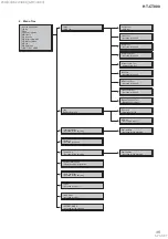
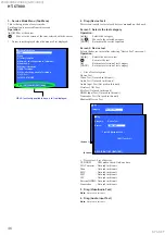
Page 34: ...ouch the 1 button to turn the power off 1 Main Functions For reference to 2 Menu Tree on page 35 Diag Performs unit test of devices installed on the board Log Error log is displayed Displayed contents can also be saved in an USB memory device Factory Initialize Not used for the servicing Network Not used in this unit Version Up Not used for the servicing System Information Displays the system info...

Page 35: ...log Diag Network 1RW XVHG in this unit HDD log Device Test 86 WHVW Video Test Not used in this unit Audio Test Not used in this unit Audio Input Test Not used in this unit Wireless LAN Test Wireless LAN test EMC Test Mode Not used for the servicing Drive Not used in this unit HDD Mode Not used in this unit Start Update Not used for the servicing Start Initialize Not used for the servicing LDJ 7HVW...

Page 36: ...electing Device Test in screen 1 Operation B b Selects the device to test Executes the test V Returns to selection of test category BACK Returns to selection of test category List of test categories Device Test Video Test Not used in this unit Audio Test Not used in this unit Audio Input Test Not used in this unit Wireless LAN Test Mic Test Not used in this unit HDMI Input Test Not used in this un...

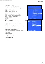
Page 37: ...gistry is OK Write Successful is displayed When write P2P address to registry is NG Write Fail is dis played Screen 3 Select 6 P2P Registry Check Check the P2P Registry address is the same as displayed in Screen 2 8 Diag Mic Test Note Not used in this unit 9 Diag HDMI Input Test Note Not used in this unit 10 Diag Transcoder Test Note Not used in this unit Diag Screen 1 Screen 2 Category Wireless L...

Page 38: ...n 4 Select 3 Write Bluetooth device address to Registry Displayed characters values in the following figure are example It records the address of the Bluetooth device Viewing the status display OK Write Successful is displayed NG Write Fail is displayed Screen 3 Diag Diag Category Bluetooth Device Test 2 Bluetooth Disable 3 Write Bluetooth device address to Registry 4 Bluetooth Inquiry Test HELP U...

Page 39: ...01 01 00 00 01 ErrCode 0A0100000000 011 2010 01 01 00 00 01 ErrCode 0A0100000000 012 2010 01 01 00 00 06 ErrCode 0902A4053002 013 2010 01 01 00 00 01 ErrCode 0A0100000000 Page 1 3 HELP Press RED key to store log to Udisc 1 Error Log 2 HDD Log Screen 1 Screen 2 13 Log HDD Log Note Not used in this unit 14 Factory Initialize Factory Settings Return all of the unit setting to their factory defaults R...

Page 40: ...T_C pin 32 and OUT_D pin 27 28 lines of IC6005 on the MB 1612 board do not short circuits or opens If there is no abnormality check the area surrounding transistor Q6004 Q6005 on the MB 1612 board Replace the IC6005 on the MB 1612 board Yes Yes Mounted parts on the OUT_A pin 39 40 OUT_B pin 35 OUT_C pin 32 and OUT_D pin 27 28 lines of IC6005 on the MB 1612 board short circuits or opens The PWM sig...

Page 41: ...CN3010 pin 15 SCL 5V pin 16 SDA 5V Continued on page 42 Yes No No No No No Check the HOT PLUG DET line The voltage of the following is about 5 0 V MB 1612 board R3223 R3226 R3229 R3230 The voltage of the following is about 3 3 V MB 1612 board Q3001 base Q3002 base Q3003 base Yes Check the area surrounding NRESET line on the MB 1612 board The voltage of the following is about 3 3 V MB 1612 board IC...

Page 42: ...92 93 In the case of HDMI IN 2 connection No Check the mounted state of connector CN3004 IC3000 and resistor RB3001 RB3002 on the MB 1612 board Yes Check the mounted state of connector CN3004 diode D5001 IC5001 and resistor R5007 R5020 on the MB 1612 board abnormality From page 41 Replace the MB 1612 board Replace the MB 1612 board Replace the MB 1612 board No abnormality Check the mounted state o...

Page 43: ...A pin 39 40 OUT_B pin 35 OUT_C pin 32 and OUT_D pin 27 28 lines of IC6005 on the MB 1612 board do not short circuits or opens If there is no abnormality replace the IC6005 on the MB 1612 board 4 Power is not turned on Power is not turned on The voltage of the following is 33 V POWER board CN904 pin 3 to 5 The voltage of the following is 12 to 18 V POWER board CN904 pin 9 The voltage of the followi...

Page 44: ...47 P0RX2P 146 P0RX2M 138 P0RXCP 137 P0RXCM 159 RX0SDA 160 RX0SCL 168 HSDA0 166 HSCL0 102 NIRQ0 88 Pana_OSD_INT 150 NOSDIRQ 167 NRESET 35 33 38 36 41 39 42 44 1 216 2 P0TX2M P0TX2P P0TX1M P0TX1P P0TX0M P0TX0P P0TXCP P0TXCM TX0SDA TX0SCL TX0HPD 100 CH0ASD0 13 Data1 99 CH0ASD1 14 Data2 98 CH0ASD2 17 SPDIF 63 CH0ASPDIF 15 Data3 97 CH0ASD3 10 BCK 65 CH0ABCLK 11 LRCK 101 CH0ALRCLK 8 MCLK 20 18 65 CSCL M...

Page 45: ...5006 27 MBA_SDA 28 MBA_SCL DATA 2 CLK 12 X1 71 X0 70 NAND_RESET 138 X5001 4MHz X401 27MHz AUDIO DIGITAL AUDIO ANALOG USB LAN WIRELESS LAN BLUETOOTH SIGNAL PATH CK DQL0 DQL7 DQU0 DQU7 A0 A13 NC J7 CK K7 CKE K9 ODT K1 ODT K1 K1 BA0 M2 BA1 N8 BA2 M3 CS L2 RAS J3 CAS K3 WE L3 DMU D3 DQSU C7 DQSU B7 DML E7 DQSL F3 DQSL G3 RESET T2 NFCEN NFREN NFWEN NFALE NFCLE NFRBN AF22 AE21 AE24 AF24 AD22 AD21 NAND F...

Page 46: ...04 SDIN1 24 SCLK 23 LRCLK 22 MCLK 11 AMP_D1 L R AMP_MCK AMP_LRCK AMP_BCK SDIN3 26 AMP_D3 AMP_D1 L R AMP_D3 AMP_BCK AMP_LRCK AMP_MCK 004B BUFFER Q6005 PWM_M_2 40 DIGITAL POWER AMP IC6005 INPUT_D OUT_D 15 INPUT_C 14 INPUT_B 6 INPUT_A 5 27 OUT_D 28 OUT_C 32 OUT_A 39 OUT_B 35 PWM_P_2 41 VALID 37 PWM_M_4 48 PWM_P_4 49 DC DETECT Q6004 16 DRIVER_CLIP OVF2 52 18 17 4 L6008 OUT_A 40 SP2 R CH MUTE PDN RESET...

Page 47: ...KEY 11 1 CS5 GPO1 TOUCH KEY 9 JL1910 VOL CS6 GPO2 TOUCH KEY 10 JL1909 CS4 GPO0 TOUCH KEY 8 JL1911 VOL 8 TS_INT 13 O LED_RESET 14 SW2 3 SW1 O LED_RESET SCL 40 NFC_CLK IRQ 35 NFC_IRQ RFDET 38 NFC_RFDET ISOLATOR PH930 SHUNT REGULATOR IC931 PROTECT DETECT Q931 BLUETOOTH INDICATOR RESET SWITCH Q5002 LINE FILTER LF901 B SWITCH Q6002 6003 B SWITCH Q301 302 OLED_12V LED_5V WS_VDD USB VBUS 3 3V FOR IC6004 ...

Page 48: ...are in Ω and 1 4 W or less unless otherwise specified 2 Nonflammable resistor 5 Fusible resistor C Panel designation A B Line Voltages are dc with respect to ground under no signal conditions no mark POWER ON Impossible to measure Voltages are taken with VOM Input impedance 10 M Voltage variations may be noted due to normal production tolerances Signal path L USB G WIRELESS LAN BLUETOOTH Note Amon...

Page 49: ... C718 R755 C719 C525 C331 JL315 CL606 R756 C526 C527 CL607 JL317 C140 CL608 C528 C334 C529 R371 R372 JL127 R373 C337 JL128 R375 X5001 JL129 R376 C722 R377 R2008 C530 R378 R2009 C531 JL321 R762 C532 C726 JL322 R763 C533 C727 R764 C534 JL131 C729 JL132 JL326 JL133 JL327 JL134 JL328 JL135 C345 JL329 JL136 C346 JL137 JL138 R384 3 2 4 1 C730 JL139 C731 C156 JL330 R771 C735 C736 JL333 JL3017 CL3038 CL30...

Page 50: ...e complete mounted board The mounted parts cannot be replaced with single for repairing 5 7 SCHEMATIC DIAGRAM USB CHUKEI Board 220p C1402 220p C1401 0 R1401 0 R1402 6 3V 220 C1403 CN1402 5P CN1401 GND 1 DP 2 DM 3 VBUS 4 GND 5 6P CN1453 RFDET 1 IRQ 2 SDA 3 GND 4 SCL 5 VDD 6 6P CN1451 1 UNSW3 3V 2 NFC_SCL 3 NFC_GND 4 NFC_SDA 5 NFC_IRQ 6 NFC_RFDET 47 RB1401 CL1453 CL1454 CL1455 CL1456 CL1451 CL1452 C...

Page 51: ...I WR3 WIFI1 WLAN BT COMBO CARD MB 1612 BOARD CN502 04P A B C D E 1 2 3 Note When the WLAN BT combo card Ref No WIFI1 is replaced refer to NOTE OF REPLACING THE MB 1612 BOARD OR WLAN BT COMBO CARD on page 5 5 9 SCHEMATIC DIAGRAM ANTTENA Section BTW WIFI 2 BOARD CHASSIS PATTERN ANTENNA FOR WIFI ANT3 ANT2 BTW WIFI 1 BOARD CHASSIS PATTERN ANTENNA FOR WIFI ANT1 BTW BT BOARD CHASSIS PATTERN ANTENNA FOR ...

Page 52: ... C1303 C1304 C1305 Q1301 CL1301 CL1302 CL1303 CL1304 CL1305 CL1306 CL1307 CL1308 CL1309 CL1310 CL1311 CL1312 CL1313 CL1314 CL1315 CL1316 CL1317 R1312 R891 3 1 R892 CN891 C891 3 1 JL891 JL892 JL893 IC891 DISPLAY BOARD SIDE A DISPLAY BOARD SIDE B 1 981 566 11 11 1 981 566 11 11 A K E TOUCH BOARD CN1901 01P MB 1612 BOARD CN5003 05P FFC2 FFC4 A B 1 2 3 4 5 SIRCS BOARD COMPONENT SIDE SIRCS BOARD CONDUC...

Page 53: ...ED_A0 DS CL1316 CL1317 CL1315 CL1309 CL1310 CL1311 CL1313 CL1314 CL1312 CL1306 CL1307 CL1308 CL1305 CL1303 CL1304 CL1301 0 R1311 0 R1310 10 C1311 R1303 330 LTC023JUBFS8TL Q1301 CL 194S HB8SP SD T D1301 R1312 0 CL1302 FB1301 0 1 C1312 FB1304 0 1 C1313 FB1302 C1310 0 1 R1313 0 FB1303 39k R1309 DISPLAY BOARD FFC2 3 4 BOARD MB 1612 LED DRIVE CN1901 FFC4 01S TOUCH BOARD E3 3V INT SCL SDA PCONT_TS DGND ...

Page 54: ... R953 R955 C952 A932 VDR901 R901 R914 CN901 CN904 R932 C905 TH901 R944 LF901 LINE FILTER C939 C940 C941 JW901 JW902 JW903 JW905 JW906 JW907 JW908 JW909 D901 C967 C969 C970 C976 C977 C980 T901 POWER TRANSFORMER D938 D966 C914 C915 C907 C988 C935 C938 C903 C990 C902 C989 POWER BOARD 1 980 471 11 11 CHASSIS K E A E A K K K K K A K A A K A A A A K K A A K K A A K K A CHASSIS US CND E3 EA3 TW US CND TW...

Page 55: ... 1 R972 C992 0 01 250V 2 5A F931 RB068L100TE25 D967 25V C969 1000 25V 1000 C970 UDZSUSTE 1730B D973 KDZVTR22B D971 35V 47 C977 0 1 C968 0 01 C971 220k R971 4 7k R978 1k R976 47k R977 10k R975 35V 47 C980 FMX 22SL D966 EL816S1 B TA DTE S PH930 4 7uH L967 E ET932 JS901 E ET931 0 5W R901 1 5M LF901 IC930 POWER CONTROL IC931 SHUNT REGULATOR POWER BOARD ISOLATOR AC IN AC1 5 10 2 14 POWER T901 6 12 13 1...

Page 56: ... Pin Function Description 3 2 1 7 3 2 3 2 3 2 0 0 0 0 3 2 3 2 0 3 2 3 2 JL1903 JL1901 CY8CMBR3108 LQXIT IC1901 CS0 PS0 1 CS1 PS1 2 CMOD 3 VCC 4 CS4 GPO0 8 CS5 GPO1 9 CS3 13 I2C_SDA 14 I2C_SCL 15 HI BUZ 16 VDD 6 VSS 7 VDDIO 5 CS6 GPO2 10 CS7 GPO3 SH 11 CS2 GUARD 12 JL1909 JL1905 JL1907 JL1910 JL1902 JL1911 MM3411A33URE IC1902 CE 1 GND 2 VOUT 3 VDD 4 6P CN1901 E3 3V 1 INT 2 SCL 3 SDA 4 PCONT_TS 5 6 ...

Page 57: ...ard IC930 STR Y6735 US CND TW IC930 STR Y6766B Except US CND TW D ST 1 S OCP 2 VCC 3 GND 4 BD 6 FB OLP 5 STARTUP LOGIC DRIVER LATCH OVERCURRENT PROTECTION BOTTOM SKIP UNDER VOLTAGE LOCK OUT REGULATOR CONSTANT CURRENT FEEDBACK STANDBY OVERLOAD PROTECTION BOTTOM DETECTION NF 7 OSCILLAOTR Ver 1 1 SYS SET 2019 09 24 22 06 08 GMT 09 00 ...

Page 58: ... input terminal 10 CS6 GPO2 I Network touch key input terminal 11 CS7 GPO3 SH I PAIRING touch key input terminal 12 CS2 GUARD I INPUT touch key input terminal 13 CS3 I Power touch key input terminal 14 I2C_SDA I O Two way I2C serial data bus with system controller 15 I2C_SCL I O Two way I2C serial data transfer clock signal bus with system controller 16 HI BUZ O Interrupt signal output to the syst...

Page 59: ...586 315 01 FOOT RUBBER 1 7 685 646 79 SCREW BVTP 3X8 TYPE2 IT 3 Ref No Part No Description Remark Ref No Part No Description Remark The components identified by mark 0 or dotted line with mark 0 are critical for safety Replace only with part number specified Les composants identifiés par une marque 0 sont critiques pour la sécurité Ne les remplacer que par une pièce por tant le numéro spécifié The...

Page 60: ...YPE 2 3 5 52 4 586 788 21 PACKING CL3 53 X 2593 931 1 CABINET TOP ASSY 54 4 586 787 11 CUSHION ABSORBENT 55 4 214 276 31 TAPE 56 4 674 137 11 SCREW PTP2X5 57 4 586 702 01 CUSHION OLED 58 4 687 629 01 W ADHESIVE TAPE 59 4 581 809 01 COVER USB FFC2 1 971 548 11 FFC 18P DISPLAY MAIN FFC4 1 971 547 11 FFC 6P DISPLAY TOUCH OLED1 1 812 049 11 ELEMENT ORGANIC EL INDICATOR SP1 1 859 160 11 LOUDSPEAKER 50 ...

Page 61: ... 107 4 966 267 12 BUSHING FBS001 CORD 108 4 586 786 91 CUSHION CL3 109 4 586 705 21 DOUBLE ADHESIVE TAPE 110 4 582 466 61 CUSHION T03 111 A 2092 220 A NFC BOARD COMPLETE 0 AC1 1 834 966 42 POWER SUPPLY CORD AEP E3 SP1 LA 0 AC1 1 835 068 21 CORD POWER AUS 0 AC1 1 837 308 12 CORD POWER SUPPLY US CND 0 AC1 1 837 312 11 CORD POWER SUPPLY AR 0 AC1 1 837 345 11 CORD POWER SUPPLY TW 0 AC1 1 837 822 21 CO...

Page 62: ... page 7 Note 2 When the WLAN BT combo card Ref No WIFI1 is re placed refer to NOTE OF REPLACING THE MB 1612 BOARD OR WLAN BT COMBO CARD on page 5 151 4 586 786 81 CUSHION CL3 152 4 586 788 11 PACKING CL3 153 4 592 179 01 CUSHION WS LABEL 154 4 564 785 11 CUSHION CZ2 A 155 4 592 083 01 SHIELD COPPER FOIL FFC1 1 971 550 11 FFC 24P AVNERATX MAIN RF1 1 492 347 21 RF MODULATOR SWA12 4V TX See Note 1 WI...

Page 63: ...LETE E3 EA3 207 4 589 900 01 SHEET RADIO WAVE ABSORPTION 208 4 586 625 11 GASKET SL 9 209 A 2178 457 A MB 1612 BOARD COMPLETE SV CH See Note 2 9 209 A 2178 458 A MB 1612 BOARD COMPLETE SV TW See Note 2 9 209 A 2178 459 A MB 1612 BOARD COMPLETE SV TH See Note 2 9 209 A 2178 460 A MB 1612 BOARD COMPLETE SV AR See Note 2 9 209 A 2178 461 A MB 1612 BOARD COMPLETE SV US CND See Note 2 9 209 A 2178 462 ...

Page 64: ...ard is replaced refer to NOTE OF REPLACING THE MB 1612 BOARD OR WLAN BT COMBO CARD on page 5 and BOND FIXED POSITION OF ELECTRICAL PARTS on page 8 Note 2 When the IC6005 on the MB 1612 board or the complete MB 1612 board is replaced refer to SPREADING OF COM POUND on page 8 When indicating parts by reference num ber please include the board name Note Due to standardization replacements in the part...

Page 65: ... TW 0 IC930 6 721 976 01 IC STR Y6766B Except US CND TW IC931 6 716 865 01 IC MM1431FNRE LINE FILTER 0 LF901 1 460 834 11 LINE FILTER 18MH MIN 1 5A US CND TW See Note 0 LF901 1 697 570 11 LINE FILTER TRANSFORMER 01C613 Except US CND TW See Note PHOTO COUPLER 0 PH930 6 600 883 01 PHOTO COUPLER EL816S1 B TA DTE S TRANSISTOR 0 Q930 8 729 056 46 TRANSISTOR 2SC5053T100Q 0 Q931 6 552 949 01 TRANSISTOR L...

Page 66: ... 11 L ch SP2 1 859 160 11 LOUDSPEAKER 50 mm 160 11 R ch WIFI1 1 493 092 21 CARD WLAN BT COMBO Wi Fi Bluetooth module See Note 3 WR1 1 849 285 11 HARNESS COAXIAL BLACK WR2 1 849 283 11 HARNESS COAXIAL GRAY WR3 1 849 284 11 HARNESS COAXIAL WHITE ACCESSORIES 4 687 591 13 MANUAL INSTRUCTION Operating Instructions ENGLISH SPANISH FRENCH US CND 4 687 591 23 MANUAL INSTRUCTION Operating Instructions ENGL...

Page 67: ...MEMO HT CT800 67 SYS SET 2019 09 24 22 06 08 GMT 09 00 ...

Page 68: ...to search for a contact point of signal lines or the like in DIAGRAMS SECTION If a contact point of a BLOCK DIAGRAM PRINTED WIRING BOARD or SCHEMATIC DIAGRAM is shown in a different page use the PDF file search function to find one e g If a contact point is shown as follow the procedure below Procedure 1 Press the F key while pressing the Ctrl key 2 Input 001Z in the search box and press the Enter...

Reviews: