– 9 –
– 10 –
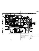
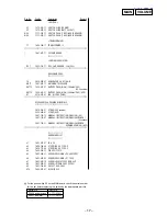
• Semiconductor
Location
Ref. No.
Location
D1
H-4
D2
F-7
D3
F-9
D4
F-8
D5
F-7
D6
E-9
D7
F-8
D8
F-7
D9
F-8
D11
B-5
IC1
F-5
IC2
D-9
IC3
E-8
Q1
F-11
Q2
G-4
Q3
H-4
Q4
C-8
Q5
D-8
Q6
D-8
Q7
E-6
Q8
E-7
Q11
E-7
Q12
H-3
Q13
E-3
ICF-B200
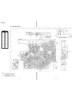
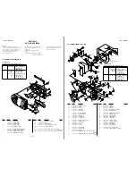
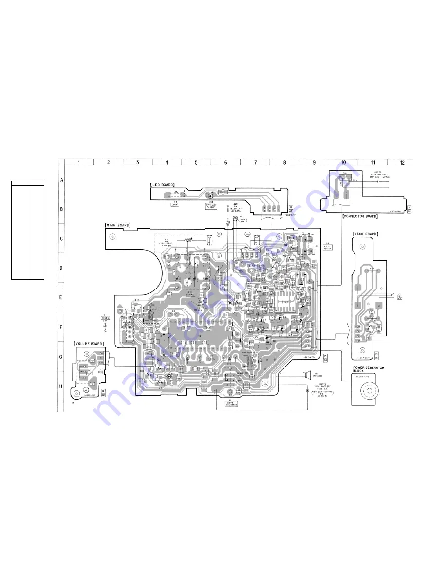
5-1. PRINTED WIRING BOARDS
Note:
•
X
: parts extracted from the component side.
•
Y
: parts extracted from the conductor side.
•
W
: indicates side identified with part number.
•
¢
: internal component.
•
b
: Pattern from the side which enables seeing.

