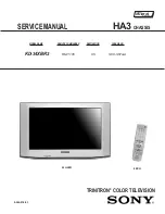
background image

TRINITRON

®

 COLOR TELEVISION


MODEL NAME


REMOTE COMMANDER


DESTINATION 


CHASSIS NO.


SERVICE 

MANUAL 


 HA3


CHASSIS

9-965-916-03

HISTORY INFORMATION FOR THE FOLLOWING MANUAL:

ORIGINAL MANUAL ISSUE DATE:  6/15/2001

ALL REVISIONS AND UPDATES TO THE ORIGINAL MANUAL ARE APPENDED TO THE END OF THE PDF FILE.

REVISION 

DATE 

  REVISION 

TYPE 

 SUBJECT     

6/2001   


No revisions or updates are applicable at this time.

10/2001 

   Re-Issue 

as 

9-965-916-02

8/2002   


Supplement - 1   

B Board, Q-Box Assembly P/N Correction; IC001 P/N Correction 
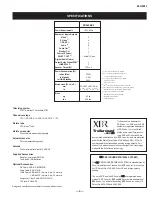


KD-34XBR2


RM-Y185 US 

SCC-S57A-A

Summary of Contents for KD-34XBR2 - 34" Hdtv Fd Trinitron Wega

Page 1: ...ORIGINAL MANUAL ISSUE DATE 6 15 2001 ALL REVISIONS AND UPDATES TO THE ORIGINAL MANUAL ARE APPENDED TO THE END OF THE PDF FILE REVISION DATE REVISION TYPE SUBJECT 6 2001 No revisions or updates are applicable at this time 10 2001 Re Issue as 9 965 916 02 8 2002 Supplement 1 B Board Q Box Assembly P N Correction IC001 P N Correction KD 34XBR2 RM Y185 US SCC S57A A ...

Page 2: ...SION SERVICEMANUAL HA3 CHASSIS KD 34XBR2 RM Y185 US SCC S57A A SelfDiagnosis Supported model 9 965 916 03 KD 34XBR2 DOLBY D I G I T A L TruSurround by SRS Trinitron RM Y185 MODEL NAME REMOTE COMMANDER DESTINATION CHASSIS NO ...

Page 3: ...ideo Sub Contrast Adjustment 29 7 4 Analog Sub Color and Sub Hue Adjustment 29 7 5 RF Sub Contrast Adjustment 30 7 6 Analog Video Sub Color and Sub Hue Adjustment 30 8 White Balance Sub Brightness and G2 Adjustments 8 1 White Balance Adjustment 31 8 2 Sub Brightness Adjustment 32 8 3 G2 Adjustment 32 SECTION TITLE PAGE 9 Safety Related Adjustments 33 10 Circuit Adjustments 10 1 Setting the Service...

Page 4: ... Optional Accessories A V Cable VMC 810 820 830HG Audio Cable RKC 515HG i LINK Cable VMC IL4415 4 pin to 4 pin 1 5 meters VMC IL4435 4 pin to 4 pin 3 5 meters Component Video Cable VMC 10 30 HG TV Stand SU 34HD2 SPECIFICATIONS SRS SOUND RETRIEVAL SYSTEM The SRS SOUND RETRIEVAL SYSTEM is manufactured by Sony Corporation under license from SRS Labs Inc It is covered by U S Patent No 4 748 669 Other ...

Page 5: ...ir deconnecte le cap de l anode court circuiter l anode du tube cathodique et celui de l anode du cap au chassis metallique de l appareil ou la couche de carbone peinte sur le tube cathodique ou au blindage du tube cathodique Afin d eviter tout risque d electrocution provenant d un chássis sous tension un transformateur d isolement doit etre utilisé lors de tout dépannage Le chássis de ce récepteu...

Page 6: ...w Leakage Test The AC leakage from any exposed metal part to earth ground and from all exposed metal parts to any exposed metal part having a return to chassis must not exceed 0 5 mA 500 microamperes Leakage current can be measured by any one of three methods 1 A commercial leakage tester such as the Simpson 229 or RCA WT 540A Follow the manufacturers instructions to use these instructions 2 A bat...

Page 7: ...ems are displayed on screen No error has occurred if the screen displays a 0 No of times STANDBY Diagnostic Item i LINK STANDBY lamp flashes Display Result Probable Cause Location Detected Symptoms Power does not turn on Does not light Power cord is not plugged in Power does not come on Fuse is burned out F6701 No power is supplied to the TV AC power supply is faulty B overcurrent OCP 2 times 2 0 ...

Page 8: ...voltage OVP Occurs when 1 overvoltage more than 140V on the B 135V line is detected by IC6505 or 2 an overvoltage more than 7 5 V on the unreg 7V line is detected by D6014 The AC relay will turn off through Q6532 and Q6530 Vertical Deflection Stopped Occurs when an absence of the Vertical deflection pulse is detected by IC201 Power supply will shut down when waveform interval exceeds 2 seconds Whi...

Page 9: ...IC5004 is 15V Care must be taken not to allow heat sink to touch any other components 2 Lift lever up on the right and left sides of the chassis bracket and gently pull the chassis assembly away from the beznet 1 1 1 1 2 1 Remove screws 15 from locations as marked 2 Gently slide the rear cover back and up to remove ...

Page 10: ...gh voltage remains in the CRT even after the power is disconnected To avoid electric shock discharge CRT before attempting to remove the anode cap Short between anode and CRT coated earth ground strap Coated Earth Ground Strap 1 2 3 4 5 6 7 8 9 10 11 12 13 14 INCORRECT CORRECT 11 Remove the degaussing coil 12 Remove the CRT grounding strap and tension springs 13 Unscrew the four CRT fixing screws ...

Page 11: ...CEDURES Turn up one side of the rubber cap in the direction indicated by arrow a Use your thumb to pull the rubber cap firmly in the direction indicated by arrow b When one side of the rubber cap separates from the anode button the anode cap can be removed by turning the rubber cap and pulling it in the direction of arrow c HOW TO HANDLE AN ANODE CAP 1 Do not use sharp objects which may cause dama...

Page 12: ...ximately 40 from 90 NOTE The rounded points 1 on the edges of each tab should be evenly aligned see the figure next column IMPORTANT Make sure that the following items are checked and adjusted whenever the CRT or Deflection Yoke have been replaced BMC Magnet 1 90 130 50 2 2 NECK ASSEMBLY POSITIONING 1 The left and right sides of the neck assembly must be straight up and down 2 Make sure that the r...

Page 13: ...rity Magnet Adjustment Tabs 3 Input a green raster from the pattern generator 4 Move the deflection yoke backwards and adjust the purity ring magnets so that the center of the screen is green and the red and blue areas on either side of the screen are approximately the same size as shown in the figure below Blue Red Green 5 Move the deflection yoke forward until the entire screen becomes green 6 C...

Page 14: ...t this point so use the sides of the raster at the half way point between the top and bottom to judge when the raster is centered Device Name Adj Item Name Data 2150D 2 0 HCEN Adjust so that the raster is centered 4 Make a note of the data that was set in step 3 5 Return all of the items adjusted in step 2 to their previous settings as follows 1 Press the 0 button READ appears in green letters at ...

Page 15: ...djust the pattern so that it is centered on the screen horizontally Do not change the HCEN data to center the pattern Use HPOS to center the pattern HCEN centers the raster HPOS centers the picture on the raster Device Name Adj Item Name Data 2150D 2 1 HPOS Adjust as necessary to horizontally center the pattern If the monoscope pattern is not available use the cross hatch pattern s center dot as t...

Page 16: ...p and bottom of the screen Device Name Adj Item Name Data 2150D 1 5 VCEN Adjust to make the bowing of the top and bottom lines equal 13 Write the data to memory 14 Adjust the vertical pin cushion Device Name Adj Item Name Data 2150D 1 6 VPIN Adjust as necessary to make the horizontal lines as straight as possible 15 Write the data to memory 16 Adjust the picture keystone Device Name Adj Item Name ...

Page 17: ... the data to memory 24 Display a cross hatch pattern do not use the monoscope pattern 25 Adjust the horizontal linearity Device Name Adj Item Name Data 2150D 2 3 SLIN Adjust as necessary so that the boxes at the left and right sides of the screen are the same width as the boxes in the middle of the screen A B A B C C 26 Write the data to memory 27 Display a cross hatch pattern do not use the monos...

Page 18: ...essary to straighten the vertical lines of the cross hatch pattern in the top and bottom corners of the screen 35 Write the data to memory 36 Display a cross hatch pattern do not use the monoscope pattern 37 Adjust the vertical keystone Device Name Adj Item Name Data 2150D 2 14 PPHA Adjust as necessary to remove vertical keystone 38 Write the data to memory 39 Display a cross hatch pattern do not ...

Page 19: ...al lines straight up and down The VBOW adjustment is effective across the entire screen 47 Write the data to memory 48 Display a cross hatch pattern do not use the monoscope pattern 49 Remove any bow from the outer vertical lines Device Name Adj Item Name Data 2150D 2 18 LBOW Adjust as necessary to make the outer vertical lines straight up and down The LBOW adjustment is most effective in the oute...

Page 20: ... menu then press the RESET button on the remote control to set the STANDARD settings to the factory settings TILT CORRECTION set to zero from the user menu VERTICAL CORRECTION set to zero from the user menu NOTE The ZOOM mode shares the adjustments made in the FULL mode As a rule you should not have to make any adjustments in ZOOM mode except vertical size ASPT and vertical position SCRL which are...

Page 21: ...ares a few of the adjustments made in the FULL mode As a rule you should not have to make any of the shared adjustments in WIDE ZOOM mode Only the adjustments listed below are necessary PROCEDURE 1 Enter the service mode 2 Display the monoscope or cross hatch pattern 3 Adjust the vertical s correction and the horizontal linearity so that the boxes in the general center area of the screen have the ...

Page 22: ...ot use the monoscope pattern 13 Adjust horizontal outer pin cushion Device Name Adj Item Name Data 2150D 2 5 PIN Adjust as necessary to straighten the vertical lines of the cross hatch pattern The PIN adjustment is more effective in the outer areas of the screen 14 Write the data to memory 15 Adjust the pincushion in the top and bottom corners of the screen Device Name Adj Item Name Data 2150D 2 7...

Page 23: ...gs TILT CORRECTION set to zero from the user menu VERTICAL CORRECTION set to zero from the user menu PROCEDURE 1 With the set turned off turn it on and tune a DTV channel either standard definition or high definition is OK then turn the set off again 2 Enter the service mode 3 Display the 1080i cross hatch pattern as follows a Select adjustment category DTV b Select adjustment item 1 PATN c Select...

Page 24: ...t to zero from the user menu VERTICAL CORRECTION set to zero from the user menu H STAT control C Board PROCEDURE 1 Make sure the TV power is off then disable the dynamic convergence circuit by unplugging CN5510 from the D board 2 Turn the set on and display the dot pattern CN5510 3 Adjust the H STAT control on the C board RV9001 to horizontally converge the red green and blue dots in the center of...

Page 25: ... assembly A plastic tuning tool is required Do not use a hex wrench as its magnetic properties will throw off the adjustment XCV Core 9 Balance any remaining misconvergence along the horizontal axis by adjusting the TLV control on the top of the yoke assembly Green and blue line up perfectly Red hangs down a small amount 10 Turn the set off and then reconnect CN5510 on the D board This completes t...

Page 26: ...and make the following adjustment Device Name Adj Item Name Data D CONV 9 CADJ Adjust as necessary so that the horizontal convergence is the same regardless if CN5510 is plugged in or not 5 Write the data to memory 6 Make sure CN5510 is plugged in 7 Remove the bow from the top and bottom of the vertical lines in the cross hatch pattern Device Name Adj Item Name Data D CONV 1 YBWU D CONV 2 YBWL Adj...

Page 27: ...BW D CONV 8 LLBW Adjust as necessary to minimize the bow separation RUBW affects this corner LLBW affects this corner RUBW affects this corner LUBW affects this corner 12 Write the data to memory 13 Check the convergence in the ZOOM WIDE ZOOM and HD1080i modes Only minor touchups are allowed as they affect the other modes Make minor adjustments as necessary as described in the sections 5 7 to 5 12...

Page 28: ...nds The 1080i pattern automatically forces the TV into the FULL mode 3 Select adjustment category 2150P 2 item 1 RGBS and change the data from 7 to 4 this turns off the blue and green 4 Select adjustment category 2150P 4 item 0 SCON and change the data so that the voltage difference between the peak white level and black level is 2 25 V 0 05 V Black VR2 VR1 White VR1 VR2 VR 2 25 V 0 05 Vp p 50mv d...

Page 29: ...data to memory 7 Select adjustment category 2150P 2 item 1 RGBS and change the data from 4 to 7 this turns the blue and green on This completes the analog video sub contrast adjustment 7 4 ANALOG VIDEO SUB COLOR AND SUB HUE ADJUSTMENT SET UP CONDITION Picture mode PRO Color Factory default press the RESET button while in PRO mode adjustment menu Picture Maximum Display mode FULL INITIAL DATA Cat 2...

Page 30: ...t category 2150P 2 item 1 RGBS and change the data from 4 to 7 this turns the blue and green on This completes the RF sub contrast adjustment 7 6 ANALOG VIDEO SUB COLOR AND SUB HUE ADJUSTMENT SET UP CONDITION Picture mode PRO Color Factory default press the RESET button while in PRO mode adjustment menu Picture Maximum Display mode TWIN mode P P INITIAL DATA Cat 2150P 1 item 4 RDRV data 45 Cat 215...

Page 31: ...ny evidence of color tinting 12 Write the data to memory 13 Change the set from the video 1 mode to the DTV mode as follows a Turn the set on and select the VHF UHF antenna b Tune the TV to channel 2 1 two point one not twenty one Use the decimal point button on the remote It s OK if there is no signal on channel 2 1 c Turn the TV off d Enter the service mode 14 Change white balance offset data fo...

Page 32: ...ollows Device Name Adj Item Name Data 2150P 1 11 SBOF 7 4 Adjust the sub bright data so that there is no light output from the CRT in the black areas of the screen Device Name Adj Item Name Data 2150P 1 3 SBRT Adjust as necessary 5 Write the data to memory This completes the sub brightness adjustment SET UP CONDITION Display mode FULL NTSC Picture mode STANDARD enter the STANDARD mode adjustment m...

Page 33: ... Vd and check hold down on the D board video with no signal standard reset mode as follows 1 Confirm B across C6544 to make sure that it is 135 3 1 Vdc 2 Confirm Vd at pin 2 CN6506 or at TP Vd for 4 3V Vd 4 65 Vdc 3 Apply 5 5 0 5 Vdc at pin 2 of CN6506 then confirm that set holds down If all adjustments are complete then seal and secure RV8001 and RV8002 with epoxy to prevent any possible misadjus...

Page 34: ...set properly as follows RESETTING THE DEFLECTION NVM DATA 1 Enter into Service Mode 2 Press 7 then MENU and then press ENTER on the remote RESETTING THE SYSTEM NVM DATA 1 Enter into Service Mode 2 Press 7 then 9 and then press ENTER on the remote RESETTING THE SYSTEM NVM DATA 1 Enter into Service Mode 2 Press 8 and then press ENTER on the remote SECTION 10 CIRCUIT ADJUSTMENTS ELECTRICAL ADJUSTMENT...

Page 35: ...LY Y C delay 0 Ref 1 30ns Y delay 2 60ns 3 100ns 0 0 The Following Data Depends on Signal Input RF CV V5 YC 6 SHAP Sharpness 0 3dB 15 3dB 6 8 4 8 7 SHF0 Sharpness F0 0 2 5MHz 1 3 0MHz 2 3 5MHz 3 4 0MHz 0 0 3 0 8 PREO Pre Over ratio 0 1 5 1 1 1 1 2 1 1 5 3 1 2 3 3 3 3 The Following Data Depends on Signal Input RF CV YC 9 BPF0 Chroma BPF F0 0 fsc 1 fsc 400k 2 fsc 800k 3 fsc 1 2M 3 0 0 10 BPFQ Chroma...

Page 36: ...run 0 0 0 19 PPHA Picture H Tim phase 0 0 5us 15 0 5us 7 7 7 The Following Data Depends on Signal Input RF V5 V6 20 CBOF Cb Ext Cb offset 0 16mV 63 16mV 34 36 32 21 CROF Cr Ext Cr offset 0 16mV 63 16mV 32 38 32 The Following Data Depends on CXA2150P 4 BLK Single BLK 0 BLK 1 BLK 2 BLK 3 22 ATPD Auto pedestal point 0 Through 1 20IRE 2 30IRE 3 40IRE 0 0 1 2 3 23 DCTR DC transfer ratio 0 100 1 95 2 90...

Page 37: ...YDLY Y C delay 0 Ref 1 30ns Y delay 2 60ns 3 100ns 0 0 The Following Data Depends on Signal Input RF CV V5 YC 6 SHAP Sharpness 0 3dB 15 3dB 2 2 7 2 7 SHF0 Sharpness F0 0 2 5MHz 1 3 0MHz 2 3 5MHz 3 4 0MHz 0 0 3 0 8 PREO Pre Over ratio 0 1 5 1 1 1 1 2 1 1 5 3 1 2 3 3 1 3 The Following Data Depends on Signal Input RF CV YC 9 BPF0 Chroma BPF F0 0 fsc 1 fsc 400k 2 fsc 800k 3 fsc 1 2M 0 0 0 10 BPFQ Chro...

Page 38: ...H25 V65 3 HV25 0 0 0 17 HMSK Mask for MacroVision 0 Off 1 On 0 1 1 18 HALI Auto H alignment 0 Off 1 On AFC free run 0 0 0 19 PPHA Picture H Tim phase 0 0 5us 15 0 5us 7 7 7 The Following Data Depends on Signal Input RF V5 V6 20 CBOF Cb Ext Cb offset 0 16mV 63 16mV 33 29 25 21 CROF Cr Ext Cr offset 0 16mV 63 16mV 33 30 25 22 2SCO SCON offset of CV for 2H Comb 0 7step 7 0step 15 8step 7 23 2SCL SCOL...

Page 39: ...The following data depends on NRMD data NRMD 0 NRMD 1 NRMD 2 NRMD 3 6 CDL Chroma delay time 0 280ns 4 0ns 7 210ns 3 3 3 3 7 DYCO Y coring level 0 Coring 0 15 Large amount of Coring 2 2 2 2 8 DYGA Y coring gain 0 0 gain 15 Maximum gain 10 10 10 10 9 DCCO C coring level 0 Coring 0 15 Large amount of Coring 5 5 5 5 10 DCGA C coring gain 0 0 gain 15 Maximum gain 5 5 5 5 11 YNRL YNR limit 0 YNR off 0 L...

Page 40: ... 86 2 4 08 3 4 22 3 3 3 3 3 3 19 YPFG Y peaking gain 0 1times 8 0times 15 0 875times 7 5 7 5 5 6 Game Pro TWIN Continued RF CV YC RF CV YC Any 18 YPFT Y peaking freq 0 3 58MHz 1 3 86 2 4 08 3 4 22 3 3 3 3 3 19 YPFG Y peaking gain 0 1times 8 0times 15 0 875times 7 5 5 5 6 20 YHCO Y coring for y 0 Off 1 Small 2 Mid 3 Large 1 21 YHCG Y coring gain for High frequency 0 Normal 1 0 5gain 0 22 HSSL Holiz...

Page 41: ... 1 The following data depends on the Video Input RF V1 CV V2 CV V3 CV V4 CV 30 NR1 Initial setting of NR On Off 0 On 1 Off 1 0 0 0 0 continued V1 YC V2 YC V3 YC V4 YC 30 NR1 Initial setting of NR On Off 0 On 1 Off 0 0 0 0 31 NR2 S N adaptive processing 0 On 1 Off 0 32 HPLL H PLLl filter 0 Slow convergence 1 Quick convergence 1 33 BPLL Burst pll filter 0 Quick convergence 1 Slow convergence 1 34 FS...

Page 42: ...mb filter 0 Narrow 1 Wide 0 0 0 37 HDP Horizontal phase 0 1 12us 4 0us 7 0 84us 4 28 BGPS Burst gate start 0 HS center 2us 15 HS center 5 75us 4 29 BGPW Burst gate width 0 0 5us 15 4 25us 10 40 TEST Test bit 0 Normal 1 Test mode 0 41 WSC Noise det Coring 0 0LSB 1 1LSB 2 2LSB 3 3LSB 1 The following data depends on the Video Input RF CV YC V5 V6 42 LIND 262P detect xx1 non st H x1x non st V 1xx LD s...

Page 43: ... 35 BDRV Bdrive gain 0 4dB 41 0dB 63 2dB 34 RCUT Rcut off 0 9dB 31 0dB 63 4dB 41 GCUT Gcut off 0 9dB 31 0dB 63 4dB 35 BCUT Bcut off 0 9dB 31 0dB 63 4dB 18 The Following Data depends on Color Temperature WARM COOL WBSW White balance offset 0 Normal 1 R100 G90 B70 1 0 SBOF Sub brightness offset Color Temp 0 7 7 0 15 8 7 7 RDOF RDRV offset 0 15 15 0 31 16 15 15 GDOF GDRV offset 0 15 15 0 31 16 18 15 ...

Page 44: ...ABL Peak ABL 0 4 9VDC 15 6 8VDC 15 SABL Signal ABL level 0 off 3 maximum gain 0 AGNG Black White aging 0 Normal 1 Black 2 White 3 Inhibit 0 AKBO AKB on off 0 on 1 off 0 The following data depends on the signal format Analog 1080i Others PT SYPH HSYNC delay 0 0 1 3 125 0 0 CLPH Clamp pulse phase 0 5 1 4 2 1 3 2 3 3 CLGA Clamp gate on off 0 Not gated 1 Gated with input HSYNC 0 0 CLSH Clamp pulse sta...

Page 45: ...llet SYSM Bandwidth 0 NTSC 1 FF 2 HD 3 DTV VMLV Not Used in HA3 VMMO VM Mode VM_LEV 0 Off 1 Low 2 Mid 3 High VMCR VM coring level 0 Off 1 5 2 10 3 15 VMLM VM limitter level 0 Off 1 83 2 67 3 50 VMF0 VM f0 0 Low 1 Mid 2 High 3 Inhibit VMDL VM delay 0 short 3 long SHOF Sharpness offset 0 0step 1 4step 2 8step 3 12step SHF0 Sharpness f0 0 Low 1 Mid 2 High 3 Inhibit PROV Pre Over Ratio 0 1 1 5 1 1 1 2...

Page 46: ...allet SYSM Band width 0 NTSC 1 FF 2 HD 3 DTV VMLV Not Used in HA3 VMMO VM Mode VM_LEV 0 Off 1 Low 2 Mid 3 High VMCR VM coring level 0 Off 1 5 2 10 3 15 VMLM VM limitter level 0 Off 1 83 2 67 3 50 VMF0 VM f0 0 Low 1 Mid 2 High 3 Inhibit VMDL VM delay 0 short 3 long SHOF Sharpness offset 0 0step 1 4step 2 8step 3 12step SHF0 Sharpness f0 0 Low 1 Mid 2 High 3 Inhibit PROV Pre Over Ratio 0 1 1 5 1 1 1...

Page 47: ...llet SYSM Band width 0 NTSC 1 FF 2 HD 3 DTV VMLV Not Used in HA3 VMMO VM Mode VM_LEV 0 Off 1 Low 2 Mid 3 High VMCR VM coring level 0 Off 1 5 2 10 3 15 VMLM VM limitter level 0 Off 1 83 2 67 3 50 VMF0 VM f0 0 Low 1 Mid 2 High 3 Inhibit VMDL VM delay 0 short 3 long SHOF Sharpness offset 0 0step 1 4step 2 8step 3 12step SHF0 Sharpness f0 0 Low 1 Mid 2 High 3 Inhibit PROV Pre Over Ratio 0 1 1 5 1 1 1 ...

Page 48: ...let SYSM Band width 0 NTSC 1 FF 2 HD 3 DTV VMLV Not Used in HA3 VMMO VM Mode VM_LEV 0 Off 1 Low 2 Mid 3 High VMCR VM coring level 0 Off 1 5 2 10 3 15 VMLM VM limitter level 0 Off 1 83 2 67 3 50 VMF0 VM f0 0 Low 1 Mid 2 High 3 Inhibit VMDL VM delay 0 short 3 long SHOF Sharpness offset 0 0step 1 4step 2 8step 3 12step SHF0 Sharpness f0 0 Low 1 Mid 2 High 3 Inhibit PROV Pre Over Ratio 0 1 1 5 1 1 1 2...

Page 49: ...et SYSM Band width 0 NTSC 1 FF 2 HD 3 DTV VMLV Not Used in HA3 VMMO VM Mode VM_LEV 0 Off 1 Low 2 Mid 3 High VMCR VM coring level 0 Off 1 5 2 10 3 15 VMLM VM limitter level 0 Off 1 83 2 67 3 50 VMF0 VM f0 0 Low 1 Mid 2 High 3 Inhibit VMDL VM delay 0 short 3 long SHOF Sharpness offset 0 0step 1 4step 2 8step 3 12step SHF0 Sharpness f0 0 Low 1 Mid 2 High 3 Inhibit PROV Pre Over Ratio 0 1 1 5 1 1 1 2 ...

Page 50: ...0 7step 7 0step 15 8step 5 Sub HUE offset from Analog 0 7step 7 0step 15 8step Vivid Pro 6 Initial Picture gain 00 15dB 63 0dB 63 31 7 Initial Brightness 00 15IRE 31 0IRE 63 15IRE 31 31 8 Initial Color 00 Color off 31 0dB 63 6dB 35 31 9 Initial Hue 00 33deg 31 Center 63 33deg 31 31 10 Initial Sharpness 00 10dB 31 2dB 63 8dB 24 31 11 Initial Color Temp 0 Low 1 Mid 2 High 3 Inhibit 2 1 12 Color axis...

Page 51: ...n the signal format and picture pallet Standard Movie Game 13 GAMM Initial Gamma 0 Weak 7 Strong Upper 2 bit 2 2 2 0 2 2 0 2 0 2 2 0 2 0 2 2 0 2 This data depends on the Service Item GAMM GAMMA CXA2150P 4 13 GSBO Sub bright offset for Gamma 0 0step 3 3step GCOO Sub color offset for Gamma 0 0step 3 3step GHUO Sub hue offset for Gamma 0 0step 3 3step This data depends on the signal format and pictur...

Page 52: ...3 85 DPIC Autopedestallevel 0 Off 1 30IREkneedown 2 35 3 40 DSBO SubbrightoffsetforUBLK 0 7step 7 0step 15 8step ABLM ABLmode 0 PIC 1 PIC BRT min 2 P B mid 3 P B max Others Small Pic ABLT CurrentdetectionVth 0 Vth0 8V 15 Vth1 9V 0 0 ABLC ABLlevel 0 Max ABL 255 Min ABL 0 0 SPOF Pictureoffsetforsmallareapicture 0 0step 31 UPIC 63 x31 0 This data depends on the signal format RF CV YC PIOF Picture off...

Page 53: ...RGN Output gain for Cr 0 2db 7 0db 15 2db 8 8 YGN Output gain for Y 0 2db 7 0db 15 2db 8 8 V SYNC sep time constant 0 6usec 3 18usec The following data depends on the signal format 1080i 720p 480p 480i HTC H SYNC sep time constant 0 for HD 1 for 15 75kHz 0 1 HWID HSEP SYNC sep type 0 Voltage slice 1 Charge Dis charge The following data depends on the signal format 1080i 720p 480p 480i HMSK H SYNC ...

Page 54: ... MVCE Analog Tuner Title MID Enhancement Service List 1 main v enhance c level code 0 7 CXD9509 HA3 MID Enhancement CXD9509 Service List 1 Applicable palllet and format The following data depends on the POP data MID 5 0 main h LPF y coefficient code 0 3 main h LPF c coefficient code 0 3 main v LPF y coefficient code 0 3 main v LPF c coefficient code 0 3 main h enhance y coreing code 0 3 main h enh...

Page 55: ...0 0 0 0 0 0 11 main h enhance c level code 0 7 0 0 0 0 0 0 0 0 0 0 12 main h enhance c coefficient code 0 1 0 0 0 0 0 0 0 0 0 0 13 main v enhance y coreing code 0 3 0 0 1 1 1 0 0 0 1 2 14 main v enhance y cliping code 0 3 0 0 1 1 1 0 0 0 1 1 15 main v enhance y level code 0 7 0 0 3 3 3 0 0 0 3 5 16 main v enhance c coreing code 0 3 0 0 0 0 0 0 0 0 0 0 17 main v enhance c cliping code 0 3 0 0 0 0 0...

Page 56: ... 0 0 1 1 11 main h enhance c level code 0 7 0 0 0 0 0 0 0 0 4 4 12 main h enhance c coefficient code 0 1 0 0 0 0 0 0 0 0 1 1 13 main v enhance y coreing code 0 3 0 0 0 1 1 0 0 0 0 0 14 main v enhance y cliping code 0 3 0 0 1 1 1 0 0 0 1 1 15 main v enhance y level code 0 7 0 0 3 3 5 0 0 0 4 4 16 main v enhance c coreing code 0 3 0 0 0 0 0 0 0 0 1 1 17 main v enhance c cliping code 0 3 0 0 0 0 0 0 ...

Page 57: ... 0 0 0 0 0 11 main h enhance c level code 0 7 0 0 0 4 4 0 0 0 0 0 12 main h enhance c coefficient code 0 1 0 0 0 1 1 0 0 0 0 0 13 main v enhance y coreing code 0 3 0 0 0 0 0 0 0 1 1 2 14 main v enhance y cliping code 0 3 0 0 0 1 1 0 0 1 1 1 15 main v enhance y level code 0 7 0 0 0 4 4 0 0 5 7 5 16 main v enhance c coreing code 0 3 0 0 0 1 1 0 0 0 0 0 17 main v enhance c cliping code 0 3 0 0 0 1 1 ...

Page 58: ... 0 0 0 1 1 11 main h enhance c level code 0 7 0 0 0 0 0 0 0 0 4 4 12 main h enhance c coefficient code 0 1 0 0 0 0 0 0 0 0 1 1 13 main v enhance y coreing code 0 3 0 0 1 1 1 0 0 0 0 0 14 main v enhance y cliping code 0 3 0 0 1 1 1 0 0 1 1 1 15 main v enhance y level code 0 7 0 0 4 7 5 0 0 4 4 4 16 main v enhance c coreing code 0 3 0 0 0 0 0 0 0 0 1 1 17 main v enhance c cliping code 0 3 0 0 0 0 0 ...

Page 59: ... 1 0 0 0 0 0 11 main h enhance c level code 0 7 0 0 0 4 4 0 0 0 0 0 12 main h enhance c coefficient code 0 1 0 0 0 1 1 0 0 0 0 0 13 main v enhance y coreing code 0 3 0 0 0 0 0 0 0 0 0 0 14 main v enhance y cliping code 0 3 0 0 1 1 1 0 0 0 0 0 15 main v enhance y level code 0 7 0 0 4 4 4 0 0 0 0 0 16 main v enhance c coreing code 0 3 0 0 0 1 1 0 0 0 0 0 17 main v enhance c cliping code 0 3 0 0 0 1 ...

Page 60: ...0 SHCL sub h enhance c cliping code 0 3 11 SHCE sub h enhance c level code 0 7 12 SHCO sub h enhance c coefficient code 0 1 13 SVYR sub v enhance y coreing code 0 3 14 SVYL sub v enhance y cliping code 0 3 15 SVYE sub v enhance y level code 0 7 16 SVCR sub v enhance c coreing code 0 3 17 SVCL sub v enhance c cliping code 0 3 18 SVCE sub v enhance c level code 0 7 Initial Data Settings 0 63 same da...

Page 61: ...ld for SNNR A B C D E F G 2 WSLT Threshold of SNNR 15 31 45 63 85 110 127 To choose the SNNR Level the following equations apply 0 WSL WSLT A Select SNNR 0 WSLT A WSL WSLT B Select SNNR 1 WSLT B WSL WSLT C Select SNNR 2 WSLT C WSL WSLT D Select SNNR 3 WSLT D WSL WSLT E Select SNNR 4 WSLT E WSL WSLT F Select SNNR 5 WSLT F WSL WSLT G Select SNNR 6 WSLT G WSL 255 Select SNNR 7 ITEM Data is controlled...

Page 62: ...ffset Data 0 0 0 0 0 0 0 0 12 5LTI CXA2150P 3 LTLV Offset Data 0 0 0 0 0 0 0 0 13 5CTI CXA2150P 3 CTLV Offset Data 0 0 0 0 0 0 0 0 14 5VMC CXA2150P 3 VMCR Offset Data 0 0 1 1 2 2 2 3 15 MIDD CXA2150P 3 MIDE offset for SN Offset Data 0 0 1 1 2 2 2 3 SNNR 0 uses no Offset Data SNNR 1 uses Offset Data 0 SNNR 2 uses Offset Data 1 SNNR 3 uses Offset Data 2 SNNR 4 uses Offset Data 3 SNNR 5 uses Offset D...

Page 63: ...HORIZONTAL TRAPEZOID 9 ZOOM ZOOM SW 10 APSW ASPECT SWITCH 1 0 11 ASPT ASPECT RATIO 0 3 12 SCRL VERTICAL SCROLL 31 31 13 UVLN 14 LVLN LOWER VERTICAL LINEARITY HA3 Deflection CXA2150D 1 Service List No ITEM NAME DESCRIPTION Initial Data Settings DESIGN PRESET DATA FACTORY ADJUSTMENT DATA WIDE ZOOM ZOOM FULL INDEX NORMAL 31 22 0 7 7 10 7 31 15 15 7 15 1 1 0 1 1 1 24 48 0 31 31 31 4 0 0 0 4 0 0 0 Titl...

Page 64: ...XCP UPPER EXTRA CORNER PIN POSITION 12 LXCP LOWER EXTRA CORNER PIN POSITION 13 XCPP EXTRA CORNER PIN POLARITY 14 PPHA PIN PHASE 15 VANG AFC ANGLE 16 LANG LINEARITY ANGLE 17 VBOW AFC BOW 18 LBOW LINEARITY BOW 19 CPY1 COPY FUNCTION 1 Refer to 1 HA3 Deflection CXA2150D 2 Service List No ITEM NAME DESCRIPTION Initial Data Settings DESIGN PRESET DATA FACTORY ADJUSTMENT DATA WIDE ZOOM ZOOM FULL INDEX NO...

Page 65: ...10 AFCM AFC LOOP GAIN 2 11 VFRQ VERTICAL FREQUENCY 12 VON VERTICAL DRIVE ON 13 JUMP REFERENCE PULSE JUMP SWITCH 14 VDJP VERTICAL DRIVE JUMP SWITCH 1 1 0 1 15 VDST VERTICAL DRIVE START SWITCH 0 0 0 1 16 EWDC PIN DC LEVEL SHIFT 17 AKBT AKB TIMING 15 9 HA3 Deflection CXA2150D 3 Service List No ITEM NAME DESCRIPTION Initial Data Settings DESIGN PRESET DATA FACTORY ADJUSTMENT DATA WIDE ZOOM ZOOM FULL I...

Page 66: ... LEVEL AT TOP BOTTOM AREA 7 DQPA DQP AMPLITUDE 8 QPAV DQP AMPLITUDE VERTICAL MODULATION 9 AVS DQP AMPLITUDE TILT 10 NORM 11 CPY3 COPY FUNCTION 2 Refer to 1 12 200V 200V REGULATOR ADJUSTMENT HA3 DF DQP CXA2026 Service List No ITEM NAME DESCRIPTION Initial Data Settings DESIGN PRESET DATA FACTORY ADJUSTMENT DATA WIDE ZOOM ZOOM FULL INDEX NORMAL 0 23 119 1 44 0 12 7 44 3 0 0 31 Title DF DQP Service L...

Page 67: ...W LEFT LOWER BOW 9 CADJ OFFSET ADJ 10 CPY2 COPY FUNCTION 2 Refer to 1 HA3 Dynamic Convergence CXA8070 Service List No ITEM NAME DESCRIPTION Initial Data Settings DESIGN PRESET DATA FACTORY ADJUSTMENT DATA WIDE ZOOM ZOOM FULL INDEX NORMAL 31 31 31 31 31 31 31 Title Dynamic Convergence Service List CXA8070 31 31 48 0 10 5 FEATURE ID MAP MODEL ID 0 ID 1 ID 2 ID 3 ID 4 ID 5 ID 6 ID 7 KD 34XBR2 89 255 ...

Page 68: ...BR2 and are not damaged corrupted the upgrade process will begin automatically The screen will display Memory Upgrade Mode for 3 seconds after which the screen will go black until the upgrade is completed NOTE The user controls are inoperative while this upgrade is in progress 4 A status LED is located above the Memory Stick slot This LED will ßash in several distinct patterns dependent upon the s...

Page 69: ...mber specified The symbol indicates a fast operating fuse and is displayed on the component side of the board Replace only with fuse of the same rating as marked The components identified by X in this basic schematic diagram have been carefully factory selected for each set in order to satisfy regulations regarding X ray radiation Should replacement be necessary replace only with the value origina...

Page 70: ...nalog Signal Flow CV CV YPbPr S Y Y C RGB YsYm RGB YsYm L Lt R Rt L Lt R Rt IN2 L Lt IN3 L Lt R Rt NJM2521 x2 IN1 IN2 IN3 Vout SW1 SW2 COMB Y C IN MON OUT EXT RGB COMB Y C IN 3Line comb Y C DC out Y VA OUT3 C CVorY CXA2150 YPbPrHV OR x4 R G B Ys RF RF Antenna SW RF AUX Q BOX R Rt CCD V CHIP ID 1 CCD V CHIP ID 1 M16C Direct View R Rt BH3868 L R L Front SP R Front SP L R Main Tuner AMP AMP VAR FIX I...

Page 71: ...6V B 1608 0 1 16V B 1608 0 47 16V B CHIP 0 0047 B 1608 0 47 16V B CHIP 0 22 16V B 1608 100 16V 0 01 25V B 1608 0 1 16V B 1608 100 16V 0 1 B 1608 0 22 B 1608 0 47 B CHIP 0 001 B 1608 1 16V F CHIP 1 16V F CHIP MA111 MA111 DAN202K OR DAN202K OR DAN202K OR MA111 MA111 MA111 PROT MA111 MA111 MA111 PROT MA111 O2CZ5 6 LIMIT MA111 ABL SW LHLZ06 LHLZ06 LHLZ06 LHLZ06 LHLZ06 LHLZ06 LHLZ06 2SD601A VIDEO BUFFE...

Page 72: ...16W CHIP 10k 1 16W CHIP 2 2k 1 16W CHIP 10k 1 16W CHIP 2 2k 1 16W CHIP 15k 1 16W CHIP 4 7k 1 16W CHIP 1k 1 16W CHIP 1k 1 16W CHIP 2 2 FPRD 2 2 FPRD 2 2 FPRD 2 2 FPRD 10k 10k 10k 10k 330k RN 330k RN 330k RN 100 RN CP 10k RN CP 15k RN CP 1k FPRD 10k CHIP 10k CHIP 22 3W 0 33 2W RS 0 33 2W RS 10 FPRD 0 CHIP 470 CHIP 10 FPRD 10k 1 16W CHIP 330k 1 16W CHIP 330k 1 16W CHIP 1k 1 16W CHIP 1 0 FPRD 1k 1 16W...

Page 73: ...04 Q4409 Q4405 Q2006 Q6004 Q6006 Q2050 Q4402 Q4401 Q3104 Q3112 Q3103 Q3106 Q6007 Q4403 Q2003 R4474 R4471 R4476 R4479 R4480 R4466 R4469 R4456 R2036 R6042 R6030 R6006 R6008 R6015 R6033 R3145 R3118 R3160 R3112 R3142 R3113 R6055 R6052 R6053 R6050 R6049 R6046 R4435 R4470 R2028 R2023 R2025 R2021 R2027 R2029 R6060 R2015 R2010 R2013 R2014 R2005 R2006 R6061 C4494 C4498 C4490 C6010 C6002 C3155 C3113 C3124 C...

Page 74: ... C3170 C3148 C3118 C3149 C3106 C3115 C3111 C3160 C3139 C3112 C3105 C3138 C3123 C3146 C3103 C3104 C3102 C3110 C3151 C3140 C3147 C3152 C3150 C3136 C3137 C3122 C3109 C2051 C2052 C6029 C6025 D4411 D4412 D4414 D4409 D2051 D2050 D2052 D3106 D3104 D3105 D3107 C4495 R3150 R3154 C3108 D3102 R3137 C3130 C3129 C3133 R3157 C3107 R3110 D3103 R3108 R3114 D6023 D6022 R6051 CN6002 CL6001 C3126 R3183 R6067 R6068 R...

Page 75: ... 0 0 26 4 6 41 GND 56 1 0 12 0 5 27 0 7 42 0 0 57 4 3 13 0 5 28 0 0 43 3 8 58 3 9 IC3101 All voltages are in V A BOARD TRANSISTOR VOLTAGE LIST 1 OF 2 B C E B C E Q2001 4 3 9 0 3 6 Q3106 4 4 8 7 3 9 Q2002 4 5 0 5 0 Q3107 2 0 GND 3 2 Q2003 0 1 7 5 GND Q3108 2 2 GND 3 2 Q2004 4 6 1 1 5 0 Q3110 2 8 11 5 0 0 Q2005 6 2 9 0 5 5 Q3111 0 0 GND Q2006 0 6 11 2 14 6 Q3112 5 6 9 0 5 0 Q2050 0 0 0 3 0 0 Q3170 0...

Page 76: ... 10 10 4 1 6 0 1 9 9 4 0 0 11 GND 2 GND 2 9 0 5 1 5 12 4 7 3 5 1 3 GND 4 2 1 IC4405 IC4406 IC6001 IC6002 All voltages are in V IC6003 IC6004 IC6005 IC6006 IC6007 IC6008 A BOARD TRANSISTOR VOLTAGE LIST 2 OF 2 B C E B C E Q4401 0 7 0 0 GND Q6002 2 6 151 8 1 5 Q4402 0 7 0 0 GND Q6003 0 2 0 0 0 0 Q4403 0 0 8 9 0 2 Q6004 0 0 5 0 GND Q4404 0 0 0 0 GND Q6005 6 2 0 2 6 3 Q4405 0 0 0 0 GND Q6006 5 0 0 0 5 ...

Page 77: ... 100 1 16W CHIP 100 1 16W CHIP 100 1 16W CHIP 100 1 16W CHIP 100 1 16W CHIP 100 1 16W CHIP 100 1 16W CHIP 100 1 16W CHIP 100 1 16W CHIP 100 1 16W CHIP 100 1 16W CHIP 100 1 16W CHIP 100 1 16W CHIP 100 1 16W CHIP 100 1 16W CHIP 100 1 16W CHIP 100 1 16W CHIP 100 1 16W CHIP 100 1 16W CHIP 100 1 16W CHIP 100 1 16W CHIP 100 1 16W CHIP 100 1 16W CHIP 100 1 16W CHIP 47 1 16W CHIP 0 47 10V B 1608 3 3k CHIP...

Page 78: ...IP 22k 1 16W CHIP 100 1 16W CHIP 22k 1 16W CHIP 100 1 16W CHIP 100 1 16W CHIP 3 9k 1 16W CHIP 680 1 16W CHIP 100 1 16W CHIP 100 1 16W CHIP 470 1 16W RN CP 470 1 16W RN CP 100 1 16W CHIP 680 1 16W CHIP 470 1 16W RN CP 470 1 16W RN CP 22k 1 16W CHIP 470 1 16W RN CP 470 1 16W RN CP 100 1 16W CHIP 22k 1 16W CHIP 15k 1 16W CHIP 680 1 16W CHIP 100 1 16W CHIP 100 1 16W CHIP 100 1 16W CHIP 680 1 16W CHIP ...

Page 79: ...W CHIP 10k 1 16W CHIP 47 1 16W CHIP 1k 1 16W CHIP 220 1 16W CHIP 220 1 16W CHIP 100 1 16W CHIP 470k 1 16W CHIP 470 1 16W CHIP 56k 1 16W CHIP 5 6k 1 16W CHIP 5 6k 1 16W CHIP 75 1 16W RN CP 100 1 16W CHIP 100 1 16W CHIP 5 6k 1 16W CHIP 100 1 16W CHIP 5 6k 1 16W CHIP 100 1 16W CHIP 100 1 16W CHIP 2 2k 1 16W CHIP 1M 1 16W CHIP 56 1 16W CHIP 470k 1 16W CHIP 1k 1 16W CHIP 2 2k 1 16W CHIP 470 1 16W CHIP ...

Page 80: ...L200 FL201 R298 L 1 0 3 R155 C 4 2 1 R476 FB502 D001 L 2 1 0 X001 C320 R330 IC001 R063 R590 FB505 FB506 R593 R595 R594 R592 FB504 L005 1 10 1 30 31 1 50 51 80 81 100 4 5 8 1 19 20 32 33 51 52 64 GND MAIN_SW B25 A25 A1 B1 GND GND GND GND GND GND GND GND GND GND GND GND GND GND GND GND GND LINE_MUTE F_SP_MUTE SEL_L SEL_R FIX VAR_L FIX VAR_R OFF_MUTE SCLK SDAT AGC_ATT MT_AFT ST_AFT MT_STR MT_SAP MODE...

Page 81: ...8 R9099 RV9001 RV9002 RV9003 D9001 D9003 D9013 D9014 D9015 D9016 D9017 IC9001 IC9002 IC9003 NL9003 R9027 C9009 C9010 330 25V 0 0047 2kV E 0 0047 500V E 0 0047 500V E 0 047 F CHIP 0 0047 500V E 30p CH CHIP JW 7 5 JW 5 10 250V HT 0 1 25V B CHIP 10 250V HT 10 250V HT 0 01 F 0 01 F 0 1 25V B CHIP 220 16V HT 0 1 25V B CHIP 0 01 F 680p 2kV B 680p 2kV B 22 250V 100 16V 10 2 2 4 7 330 25V 220 16V 0 1 25V ...

Page 82: ...5 R9071 R9087 R9016 R9086 R9070 R9014 R9089 RV9003 C9046 EY9014 JW9005 JW9006 EY9012 C9012 C9022 D9006 EY9009 C9031 R9056 L9005 JW9017 R9085 CLP9003 R9077 D9008 CN9002 CN9006 CN9003 CN9004 R9088 JW9014 J 9 0 0 1 RV9001 EY9015 EY9011 R9009 R9050 C9005 R9024 NL9003 C9004 EY9007 R9054 EY9013 R9038 C9003 JW9008 JW9012 JW9004 JW9009 C9017 C9033 RV9002 CN9001 Q9008 Q9012 D9015 D9017 D9016 Q9002 JW9001 J...

Page 83: ...111 1 1UH 0 45UH 1 1UH 0 45UH 0 45UH MCZ3001D DRIVER DM 58 CONTROL 0 CHIP 7 5MM 7 5MM LHL08 LHL08 LHL10 ON3171 R RESISTOR SHORT ON3171 R MAIN CONTROL ICP N70 ICP N70 2SD601A IRFIB7N50A CONVERTER IRFIB7N50A CONVERTER 2SA1208S B OCP 2SA1309A OCP LATCH 2SB709A LATCH 2SD2114 AC RLY DRV 2SD601A VC SW 2 2SD601A LATCH 2SB709A LATCH 2 2SD601A MAIN SW 2SD601A LATCH 1 91 RN CP 470k 1 2W 100 RN CP 10k CHIP 0...

Page 84: ... 9B REF VOLT RGP02 20EL G2 RECT RGP10G PROTECT D5LC20U HEATER RECT RGP10G 200V RECT ERC91 02 CENT VEE ERC91 02 CENT VCC MTZJ 15B CLAMP MA111 PROT MA111 PG124S15 DUMPER MA111 MA111 MA111 MA111 MA111 MA111 PROTECT MA111 TEMP C MA111 TEMP C MA153 PROT MA111 MA153 PROT D1NL20 DQP SW D1NL20 PEAK DET MTZJ 12 PROT MTZJ 12 PROT 1 1UH NJM2903M PWM CONT STV9379 V OUT PQ6RD83B HEATER OUT NJM2901M H PROT CONT...

Page 85: ...0p 2kV B 0 1 PT 0 022 630V PP 10 100p 500V B 220p 500V B 0 01 B CHIP 0 47 MPS 47 10V 4 7 160V 0 01 630V MPS MA111 LATCH 2 MA111 STOPPER MTZJ 5 1B IK PROT REF MA111 IK PROT2 SW MTZJ 13C LIMIT MA111 IK PROT1 SW D1NL20U STOPPER RGP10G ERA22 08TP3 SNUBBER MTZJ 15B MA111 MA111 MA111 MA111 MA111 0 45UH NJM2901M PROT DETECT 1 MCZ3001D DRIVER NJM2904M BUFF 0 CHIP 0 CHIP 0 CHIP 0 CHIP 0 CHIP 0 CHIP 0 CHIP ...

Page 86: ...R5039 C5044 R5030 R5035 R5048 R5042 R5045 C5511 C5018 C5012 R5055 R5040 R5150 R5001 R5125 C5076 C5077 C5079 C5046 D5027 R5108 C5051 C5052 C8025 C8027 C8031 C8033 C8042 D8010 D8012 L8002 L8003 R8049 R8050 R8051 R8057 R8058 R8059 R8060 R8062 R8066 R8079 R8081 R8083 C8037 C8030 R8056 R8055 R8069 C5026 R5013 R5073 R5074 R5075 R5004 R5007 R5008 R5011 R5012 R5014 R5078 Q5004 R5504 R5505 C8034 C8024 C503...

Page 87: ...4 L6503 C6547 D6517 R5135 Q6521 Q6522 Q6524 C6592 C6595 D5025 C6585 R6510 C6591 PS6501 R6614 PS6502 R5142 R5145 R6539 FB6501 FB6504 R5712 R5711 C5999 CLP5001 C6505 C6506 C8070 R5164 R8199 D8028 SG8005 D8050 D8051 CN5501 JL1 JL2 C5080 C5081 FB6505 C5011 1 12 G S B V PROT 2 1 1 9 10 18 E B E B 1 2 3 4 1 2 3 4 1 2 3 4 1 8 1 8 1 8 1 9 10 18 1 2 3 4 G S G S E B E B E N C N C S C P R B E B INT C L K 1 S...

Page 88: ... 15 7 6 0 0 18 1 7 3 GND 7 4 0 8 17 2 pin volt 9 GND 1 134 0 10 10 4 2 N C IC6505 IC6503 IC6501 All voltages are in V B C E Q6503 0 0 2 5 0 0 Q6520 131 0 0 0 132 0 Q6521 0 0 2 1 GND Q6522 15 7 GND 15 7 Q6524 2 1 0 4 4 9 Q6526 5 9 0 0 5 9 Q6527 0 6 0 0 0 0 Q6528 0 6 0 0 0 0 Q6529 0 0 5 9 0 0 Q6530 4 7 0 0 4 7 Q6531 0 6 0 0 GND Q6532 0 0 4 7 GND D G S Q6506 4 7 149 2 0 0 Q6507 154 4 303 3 150 0 All ...

Page 89: ... 2 10 1 4 8 1 0 2 4 6 4 4 6 8 2 7 2 15 6 11 6 1 9 1 0 3 4 0 5 5 0 9 GND 3 12 6 12 GND 10 0 0 4 4 2 6 5 0 4 14 5 13 2 5 11 0 0 5 9 0 7 N C IC5514 IC5515 IC5511 All voltages are in V IC5512 IC5513 IC5502 IC5504 IC5506 IC5510 IC5006 IC5005 IC5007 IC5008 IC5501 IC5004 IC5001 IC5002 IC5003 D BOARD IC VOLTAGE LIST 2 OF 3 D BOARD TRANSISTOR VOLTAGE LIST 2 OF 3 B C E B C E B C E B C E Q5001 2 9 12 0 3 3 Q...

Page 90: ...5 0 1 1 6 12 4 5 3 11 0 7 0 0 2 1 8 13 N C 8 5 0 3 2 2 14 104 8 pin volt 9 4 2 4 2 5 15 94 8 1 14 0 IC8004 All voltages are in V IC8001 IC8002 IC8003 B C E Q8001 0 1 0 0 GND Q8002 0 0 1 6 GND Q8003 0 2 1 6 GND Q8004 0 0 1 6 GND Q8007 0 6 0 0 GND Q8008 0 6 0 0 GND Q8009 196 0 0 0 196 0 Q8010 2 1 0 0 GND Q8015 0 5 0 0 GND Q8016 134 5 134 7 135 1 Q8018 5 5 94 4 GND Q8019 3 5 0 0 GND Q8020 0 0 0 5 GND...

Page 91: ...HT MINI 3P WHT MINI LOCK 3P WHT MINI LOCK 8P WHT S MICRO 1P TAB CONTACT 1P TAB CONTACT 2P WHT PW CN SBT LFC LFC 2SC3311A DGC RLY DRV 1SS133 AC OFF DET 1SS133 AC OFF DET E E F O R C H E C K AC DET STBY 15V E STBY 7V E CHECK CHECK DGC NC DGC DGC NC DGC DGC RLY E SUB 12V AC L AC N AC N AC L TO A CN6002 AC IN DGC DGC DGC DGC CN6009 TO A BOARD TO A BOARD CN6010 TO D BOARD CN6502 AC DGC STANDBY 9 965 91...

Page 92: ...S09 S10 S11 S08 R23 R24 R25 CN01 10 LNK0120022G1 SPR 325MVW RD5 6ES T1B2 PROTECT IC SBX3081 01 20 10k 2 2 100 22k 4 7k RN 10k RN 3 3k RN 1 8k RN 1 5k RN 1 2k RN 820 RN 680 RN 560 RN 390 RN 470 RN 1 2k 1 8k JW 5 12P WHT S MICRO KEY INPUT LED RMC VOL CH TV VIDEO SELECT RIGHT DOWN UP LEFT MENU TO A BOARD CH VOL TIMER P SW P SW P ON SIRCS STBY 5V GND REPEAT LED STBY LED TIMER LED GND KEY GND STBY ILIN...

Page 93: ... 3 4 5 6 7 8 C4600 C4601 C4602 C4603 CN4600 FL4600 FL4601 FL4602 J4600 R4600 R4601 R4602 R4603 R4606 R4607 VD4600 VD4601 VD4602 VD4603 VD4604 VD4605 C4604 1 1 0 47 0 47 11P WHT S MICRO EMI FILTER EMI FILTER EMI FILTER 470k CHIP 470k CHIP 75 RN CP 75 RN CP 1k CHIP 75 RN CP 7 5V 1608 7 5V 1608 7 5V 1608 7 5V 1608 7 5V 1608 7 5V 1608 0 1 25V B CHIP SW2 FR C IN GND FR R IN GND FR Y IN GND FR L IN GND ...

Page 94: ...ML 210MT T86 GREEN SML 210MT T86 GREEN SML 210MT T86 GREEN SML 210MT T86 GREEN SML 210MT T86 3 3V GREEN SML 210MT T86 GREEN SML 210MT T86 GREEN 0 0 0 TC74L CX541FT EL LED BUFFER 3 3V LINK_XRST PHY_XRST 1394BIAS_SW 3 3V XRST 27MCLK 5V FLASH_MODE CYCLE_OUT XIRQ2 DMXI_BUS TSD_BUS EBBUS HBBUS SYNC_XRESET PERRORIN PERROROUT 8 1 7 2 6 3 5 4 8 1 7 2 6 3 5 4 TSOUT0 TSOUT1 TSOUT2 TSOUT7 TSDIN0 TSDIN1 TSDIN...

Page 95: ...6 1 16W 5 1k 1 16W 56 1 16W 10k 1 16W 10k 1 16W 10k 1 16W 22 22 56 56 22 22 22 22 1000 50V B CHIP 1000 50V B CHIP MA152WA TX ACM2012 201 2P ACM2012 201 2P ACM2012 201 2P ACM2012 201 2P 0 0 0 OUH OUH 0 1 25V F 82p 50V CH 0 1 25V F 0 1 25V F 0 1 25V F 0 1 25V F 0 1 25V F 0 0 LM358P WR 12 0 1 25V F 0 1 25V F CXD1945R LINK PHYSICAL LAYER IC CXD3203R LINK LINK LAYER LSI 2SD2216J CABLE BIAS 10k 1 16W PH...

Page 96: ...YSCMD4 SYSCMD3 SYSCMD2 SYSCMD1 SYSCMD0 SD_D15 SD_D14 SD_D13 SD_D12 SD_D11 SD_D10 SD_D9 SD_D8 XBE1 SD_A11 SD_A9 SD_A8 SD_A7 SD_A6 SD_A5 SD_A4 SD_D0 SD_D1 SD_D2 SD_D3 SD_D4 SD_D5 SD_D6 SD_D7 XBE0 SD_A13 SD_A12 SD_A10 SD_A0 SD_A1 SD_A2 SD_A3 TDO SD_D15 SD_D14 SD_D13 SD_D12 SD_D11 SD_D10 SD_D9 SD_D8 SD_A13 SD_A12 SD_A11 SD_A10 SD_A9 SD_A0 SD_A1 SD_A2 SD_A3 SD_A4 SD_A5 SD_A6 SD_A7 SD_A8 EBA11 EBA10 EBA...

Page 97: ...ELEASE 3 3V 3 3V 3 3V XRST XRST CPU_XINT ROM_BUS 25MHZ_B TCLOCK JTAG_BUS 3 3V 3 3V 3 3V HBBUS SYNC_XRESET 3 3V SYSAD0 SYSAD1 SYSAD2 SYSAD3 SYSAD4 SYSAD5 SYSAD6 SYSAD7 SYSAD8 SYSAD9 SYSAD10 SYSAD11 SYSAD12 SYSAD13 SYSAD14 SYSAD15 SYSAD16 SYSAD17 SYSAD18 SYSAD19 SYSAD20 SYSAD21 SYSAD22 SYSAD23 SYSAD24 SYSAD25 SYSAD26 SYSAD27 SYSAD28 SYSAD29 SYSAD30 SYSAD31 SYSCMD0 SYSCMD1 SYSCMD2 SYSCMD3 SYSCMD4 TMS...

Page 98: ...RN CP 22 22 22 22 22 22 22 22 10k 10k 10k 470 1 16W CHIP 0 060 CHIP 47 16V AL CP 100 10V AL CP 100 10V AL CP 10 50V AL CP 47 16V AL CP 0 1 25V F CHIP 0 1 25V F CHIP MA2S111 TX MA2S111 TX MA2S111 TX 100P PLUG 1 4A CHIP 10V B CHIP 10V F CHIP 6 3V B CHIP 10V B CHIP 10V B CHIP 10V F CHIP 6 3V B CHIP 6 3V B CHIP 6 3V B CHIP 0 1 16W 0 1 16W CHIP 0 1 16W CHIP 0 1 16W 0 1 16W CHIP 0 015 CHIP 68k 1 16W RN ...

Page 99: ...RAS0 XMEMCSROM XMEMRAS2 XMEMBE3 XMEMBE2 XMEMBE1 XMEMBE0 XAUDCS XVIDCS TDO XTRST TCK TMS TDI TRIGOUT TDO TDI TCK TMS TRIGIN TRIGOUT DIAG TXD DIAG RXD XMEMOE MEMRXW XVIDIRQ XAUDIRQ XVIDCDRQ XAUDCDRQ XVIDCDST XAUDCDST XTRST TRIGIN DIAG TXD DIAG RXD MEMADR17 MEMADR16 MEMADR15 MEMADR14 MEMADR13 MEMADR12 MEMADR11 MEMADR10 MEMADR21 MEMADR20 MEMADR19 MEMADR9 MEMADR8 MEMADR7 MEMADR6 MEMADR5 MEMADR4 MEMADR3...

Page 100: ...HIP 3300p 50V B CHIP 3300p 50V B CHIP 3300p 50V B CHIP 3300p 50V B CHIP 47 1 16W CHIP 47 1 16W CHIP 47 1 16W CHIP 0 1 16W CHIP CHIP CHIP 10 10V F CHIP 10 10V F CHIP 10 10V F CHIP 100 1 16W CHIP 0 1 25V F 1608 10k 1 16W CHIP 10 6 3V B CHIP STI4600BCV 2 0 AUDIO DECODER TC7SET08FU TE85R OPTICAL MUTE GP1FH500TZ OPTICAL OUT 6 3V AL CP 4 7 1 16W CHIP 100 1 16W CHIP 0 CHIP 0 1 25V F CHIP 47 CHIP 10 1 16W...

Page 101: ...41 VIDMD42 VIDMD43 VIDMD44 VIDMD45 VIDMD46 VIDMD47 VIDMD48 VIDMD49 VIDMD50 VIDMD51 VIDMD52 VIDMD53 VIDMD54 VIDMD55 VIDMD56 VIDMD57 VIDMD58 VIDMD59 VIDMD60 VIDMD61 VIDMD62 VIDMD63 VIDMD4 VIDMD0 VIDMD1 VIDMD2 VIDMD3 VIDMD5 VIDMD6 VIDMD7 VIDMD8 VIDMD9 VIDMD10 VIDMD11 VIDMD12 VIDMD13 VIDMD14 VIDMD15 VIDMD16 VIDMD17 VIDMD18 VIDMD19 VIDMD20 VIDMD21 VIDMD22 VIDMD23 VIDMD24 VIDMD25 VIDMD26 VIDMD27 VIDMD28...

Page 102: ... 1 16W CHIP 100 1 16W CHIP 100 1 16W CHIP 10k 1 16W CHIP 0 1 16W CHIP 470 1 16W CHIP 470 1 16W CHIP 470 1 16W CHIP 470 1 16W CHIP 33 1 16W CHIP 33 1 16W CHIP 3 6M 3 6M 22 1 16W CHIP 22 1 16W CHIP 10k 1 16W CHIP TLC2933IPWR 12 READ PLL TLC2932IPWR WRITE PLL 2SB1462J TX VCO LIM 2SD2216J TX VCC DROP 47 47 47 47 47 47 47 47 47 47 100 1 16W CHIP 100 1 16W CHIP 1 3k RN CP 1 2k RN CP 1 3k RN CP 1k CHIP C...

Page 103: ...H CHIP 2SC2223 BUFFER 2SC2223 BUFFER 2SC2223 BUFFER 17M LPF 17M LPF 34M LPF 0 1 16V B CHIP 0 1 16V B CHIP 0 1 16V B CHIP 300 1 16W RN CP 300 1 16W RN CP 200 1 16W RN CP 300 1 16W RN CP 300 1 16W RN CP 200 1 16W RN CP 3k 1 16W RN CP 0 1 25V F CHIP 22 1 16W CHIP 22 22 22 22 22 22 47 16V AL CP 1 6 3V B CHIP CHIP 47 16V AL CP 0 1 25V F CHIP 100 6 3V AL CP 3 3k 1 16W RN CP 1k 1 16W RN CP 3 3k 1 16W RN ...

Page 104: ...MSK_PLD SYNCSW 8 1 7 2 6 3 5 4 8 1 7 2 6 3 5 4 8 1 7 2 6 3 5 4 8 1 7 2 6 3 5 4 4 5 3 6 2 7 1 8 4 5 3 6 2 7 1 4 5 6 2 7 1 4 5 6 2 7 1 4 5 6 2 7 1 4 5 6 2 7 1 4 5 6 2 7 1 4 5 6 2 7 1 8 1 7 2 6 3 5 4 8 1 7 2 6 3 5 4 8 1 7 2 6 3 5 4 8 1 7 2 6 3 5 4 8 1 7 2 6 3 5 4 8 3 8 3 3 8 3 8 3 8 3 8 Y1 Y2 Y3 Y4 Y5 Y6 Y7 CR0 CR1 CR2 CR3 CR4 CR5 CR6 CR7 CB0 CB1 CB2 CB3 CB4 CB5 CB6 CB7 Y0 Y1 Y2 Y3 Y4 Y5 Y6 D0 D1 D2 ...

Page 105: ...VRST YGVCTRL MICON_RST DIAG MID_BUSY M2 XSYNC AUD27MHZ GRANT D3 3V XYGV H XTV H YGVGCK 8 1 7 2 6 3 5 4 8 1 7 2 6 3 5 4 8 1 7 2 6 3 5 4 8 1 7 2 6 3 5 4 8 1 7 2 6 3 5 4 8 1 7 2 6 3 5 4 8 1 7 2 6 3 5 4 8 1 7 2 6 3 5 4 8 1 7 2 6 3 5 4 8 1 7 2 6 3 5 4 8 1 7 2 6 3 5 4 8 1 7 2 6 3 5 4 C7 C6 C5 C4 C3 C2 C1 C0 Y7 Y6 Y5 Y4 Y3 Y2 Y1 Y0 Y0 Y1 Y2 Y3 Y4 Y5 Y6 Y7 C0 C1 C2 C4 C5 C6 C7 DQ3 DQ0 DQ1 DQ2 DQ4 DQ5 DQ6 ...

Page 106: ... 10k 1 16W CHIP 10 1 16W CHIP 10k 1 16W CHIP 10k 1 16W CHIP 4 7k 1 16W CHIP 4 7k 1 16W CHIP 22k 1 16W CHIP 22k 1 16W CHIP 0 1 25V F CHIP 1 8k 1 16W CHIP 3 3k 1 16W CHIP 10k 1 16W CHIP 4 7k 1 16W CHIP 47k 1 16W CHIP 10 1 16W CHIP MB94P918PF G MID UCOM 0 1 25V F CHIP 1 6 3V B CHIP MA2S111 TX M24C32 WMN6T A MIDX NVM 2SD2216J TX INVERTER TC74LVX157FT EL SYNC SELECT 2SD2216QR TX INVERTER 2SB1462J TX PU...

Page 107: ... 20 SYSTEM MICRO AUDIO VIDEO DECODE MPEG AD DRC HD ADC MID XA YGV GRAPHICS MID UCOM QM QI BOARDTO BOARD CONNECTOR LINK AND PHY B CHIP AND SDRAM FLASH AND PROM COMPONENT SIDE 1 2 3 4 5 A B C D E F G H I 1 2 3 4 5 6 7 8 9 10 A B C D E F G H I ...

Page 108: ...TOR LINK AND PHY B CHIP AND SDRAM FLASH AND PROM CONDUCTOR SIDE 1 2 3 4 5 A B C D E F G H I CONDUCTOR SIDE FE PS ST 20 SYSTEM MICRO AUDIO VIDEO DECODE MPEG AD DRC HD ADC MID XA YGV GRAPHICS MID UCOM QM 1 2 3 4 5 6 7 8 9 10 A B C D E F G H I ...

Page 109: ...00 1 16W CHIP 100 1 16W CHIP 4 7k 1 16W CHIP 1M 1 16W CHIP 1M 1 16W CHIP 39k 1 16W CHIP 39k 1 16W CHIP 47 1 16W CHIP 47k 1 16W CHIP 22k 1 16W CHIP 33k 1 16W CHIP 39k 1 16W CHIP 0 1 16W CHIP 39k 1 16W CHIP 39k 1 16W CHIP 0 1 16W CHIP 470 1 16W CHIP 470 1 16W CHIP 1k 1 16W CHIP 0 1 16W CHIP NJM2181M TRUSURROUND NJM4558E V F BUFFER NJM4558E WOOFER LPF 62k CHIP 47k CHIP 39k 1 16W CHIP 22k CHIP 4 7k CH...

Page 110: ... C4470 C4459 C4467 C4464 C4461 C4472 C4474 C4476 C4468 C4469 L4402 C4416 C4415 C4429 C4432 C4446 C4442 C4441 C4434 C4447 C4448 C4460 C4449 C4414 C4413 C4443 C4433 C4420 C4419 C4422 C4401 C4410 C4418 C4427 C4445 C4475 C4425 C4424 CN4401 IC4403 R4416 R4417 R4418 R4421 R4410 R4411 R4404 R4407 R4440 R4413 R4439 R4409 R4442 R4453 R4414 R4412 R4408 R4434 R4441 R4459 R4450 R4448 R4468 C4404 C4409 C4406 C...

Page 111: ...W RN CP 75 1 16W RN CP 470k 1 16W RN CP 470k 1 16W RN CP 75 1 16W RN CP 75 1 16W RN CP 75 1 16W RN CP 470k 1 16W CHIP 470k 1 16W CHIP 75 1 16W RN CP 75 1 16W RN CP 75 1 16W RN CP 470k 1 16W CHIP 470k 1 16W CHIP 75 1 16W RN CP 75 1 16W RN CP 1k 1 16W CHIP 75 1 16W RN CP 470k 1 16W CHIP 470k 1 16W CHIP 75 1 16W RN CP 75 1 16W RN CP 75 1 16W RN CP 470k 1 16W CHIP 470k 1 16W CHIP 100 1 16W CHIP 100 1 ...

Page 112: ...GND GND GND GND GND GND GND GND GND GND GND GND GND GND GND GND GND GND GND GND FIX VAR FIX VAR L R FIX VAR R C3 C1 C4 VIDEO 5 VIDEO 6 1 681 831 11 172001311 1 2 3 4 5 6 7 8 9 10 11 12 13 14 15 16 17 18 19 20 21 22 23 24 25 26 27 28 29 30 31 32 33 34 35 36 37 38 39 40 41 42 43 44 45 46 47 48 49 50 51 52 53 54 55 56 57 58 59 60 61 62 63 64 J4002 J4008 J4004 J4005 J4001 J4009 J4003 C4003 C4008 C4004...

Page 113: ... 1 1 4W FPRD 0 47 250V MP 100 1 16W CHIP 1 1UH 1 1UH 47 1 16W CHIP 47 1 16W CHIP 180k 1 16W CHIP 47 1 16W CHIP 47 1 16W CHIP 0 1 250V MP 4 7k 1 16W CHIP 4 7k 1 16W CHIP 180k 1 16W CHIP 0 0047 500V E 2SD601A BUFF 2SD601A BUFF 0 1 250V MP 0 1 25V F 1608 0 1 25V F 1608 2SD601A BUFF 2SD601A BUFF 2SD601A BUFF 2SD601A BUFF 0 1 25V F 1608 150k 1 16W CHIP 150k 1 16W CHIP 100 16V 10 160V 10 50V 1000p 50V B...

Page 114: ...L P 9 1 0 1 C 9 1 0 4 C 9 1 0 8 C 9 1 0 9 C9114 C9113 C9115 C 9 1 0 3 C9111 C9101 C 9 1 1 7 C 9 1 0 2 FB9101 F B 9 1 0 0 J W 9 1 0 0 L 9 1 0 0 Q 9 1 1 1 Q 9 1 1 0 R 9 1 0 2 R9113 R9112 R9114 R9117 R9116 R9119 R9118 R 9 1 2 8 EY9100 EY9101 EY9102 EY9103 J W 9 1 0 1 JW9102 C N 9 1 0 2 C N 9 1 0 1 C N 9 1 0 0 C N 9 1 0 3 R9115 1 1 2 1 3 1 3 B E B E 135V VM E E V PIN V PIN NC V PIN V PIN Q P Q P Q P Q...

Page 115: ... 50 51 80 81 100 INDEX CXA2150Q 28pin CXD2057M T6 TEA6422DT 16pin CXD2085M T4 SN74LV4053ANSR 208pin CXD2090Q 240pin CXD9509AQ TOP VIEW 1 22pin CXA2026AS M52055FP MC74HC4066F TLC2932IPW TLC2933IPWR 12 14pin 86pin MB81F643242B 10FN TOP VIEW 30 1 31 50 51 80 81 100 INDEX MB94918 DX1MID M306V2ME 102FP TOP VIEW 1 18pin MCZ3001D 50pin MSM56V16160F 10TS K BH3868AFS E2 1 TOP VIEW 64pin TLC5733AIPM PST9120...

Page 116: ... C E 2SC4632LS CB7 2SK1572S 2SK2036 TE85L PQ09RD21 PQ05RF21 PQ09RF21 PQ12RF21 PQ30RF21 D S G B C E UPC1093J 2SC3997S SONY B E C 2SA2005 2SC5511 G D S DTA114EKA T146 DTA143EK DTA144EKA T146 DTC114EK E LETTER SIDE C B 1 1 2 3 4 3 4 PC123FV2 5 1 LA6500 FA NJM79M12FA DTC114TKA T146 DTC143EKA T146 DTC144EKA T146 2SA1162 G 2SA1226 2SC1623 L5L6 2SC4081 R 2SD601A Q 2SD601A Q TX 2SD601A S SEMICONDUCTORS co...

Page 117: ...these components 13 1 PICTURE TUBE 1a 4 080 281 04 BEAM 1b X 4038 679 3 SPACER 36 ASSY 2 X 4038 670 2 HOLDER DGC ASSY 3 8 735 060 05 CRT 36RV2 4 4 064 944 01 SUPPORTER CRT 5 4 053 005 01 SPACER DY 6 4 083 414 01 PIECE A 110 CONV CORRECT 7 1 452 032 00 MAGNET DISC 8 4 051 734 21 PIECE B 120 CONV CORRECT 9 8 451 498 22 DY Y36RVC M2 REF NO PART NO DESCRIPTION REF NO PART NO DESCRIPTION 9 10 11 12 13 ...

Page 118: ... POWER WITH CONNECTOR 38 8 598 542 20 TUNER FSS BTF WA412 39 8 598 542 20 TUNER FSS BTF WA412 40 1 555 400 00 CABLE PIN 13 2 CHASSIS REF NO PART NO DESCRIPTION REF NO PART NO DESCRIPTION Assembly Includes 51 50 52 20 26 38 23 27 29 25 24 22 31 36 37 34 33 35 30 33 44 43 45 42 40 41 46 47 48 49 28 21 53 54 55 56 39 41 1 557 056 31 CABLE P P 42 1 453 346 11 FBTASSY NX 6000 JIJ4 43 44 43 1 900 805 19...

Page 119: ...70 62 4 076 673 03 DAMPER DOOR 63 4 072 630 01 CUSHION DOOR 64 4 080 379 31 DOOR 65 4 080 364 11 BUTTON POWER 66 4 042 593 01 SPRING COMPRESSION 67 3 704 179 01 EMBLEM NO 9 SONY 68 4 080 363 11 BUTTON MENU 69 4 080 362 11 BUTTON MULTI REF NO PART NO DESCRIPTION Assembly Includes REF NO PART NO DESCRIPTION Assembly Includes 70 4 080 361 11 GUIDE LED 73 4 081 324 01 DAMPER DT 74 X 4039 164 1 HANDLE ...

Page 120: ... 164 156 11 CERAMIC CHIP 0 1µF 25V C030 1 126 933 11 ELECT 100µF 20 16V C031 1 164 156 11 CERAMIC CHIP 0 1µF 25V C034 1 164 156 11 CERAMIC CHIP 0 1µF 25V C035 1 162 910 11 CERAMIC CHIP 5pF 0 25pF 50V C036 1 162 919 11 CERAMIC CHIP 22pF 5 50V C037 1 162 919 11 CERAMIC CHIP 22pF 5 50V C100 1 164 156 11 CERAMIC CHIP 0 1µF 25V C101 1 164 156 11 CERAMIC CHIP 0 1µF 25V C102 1 164 156 11 CERAMIC CHIP 0 1...

Page 121: ... 16V C259 1 126 963 11 ELECT 4 7µF 20 50V C260 1 126 933 11 ELECT 100µF 20 16V C261 1 164 156 11 CERAMIC CHIP 0 1µF 25V C262 1 107 826 11 CERAMIC CHIP 0 1µF 10 16V C263 1 107 826 11 CERAMIC CHIP 0 1µF 10 16V C264 1 107 826 11 CERAMIC CHIP 0 1µF 10 16V C265 1 107 826 11 CERAMIC CHIP 0 1µF 10 16V C266 1 107 826 11 CERAMIC CHIP 0 1µF 10 16V C267 1 107 826 11 CERAMIC CHIP 0 1µF 10 16V C268 1 126 933 1...

Page 122: ... 964 11 ELECT 10µF 20 50V C414 1 164 156 11 CERAMIC CHIP 0 1µF 25V C415 1 126 935 11 ELECT 470µF 20 16V C416 1 164 156 11 CERAMIC CHIP 0 1µF 25V C417 1 164 156 11 CERAMIC CHIP 0 1µF 25V C418 1 164 156 11 CERAMIC CHIP 0 1µF 25V C419 1 126 964 11 ELECT 10µF 20 50V C420 1 125 891 11 CERAMIC CHIP 0 47µF 10 10V C421 1 164 156 11 CERAMIC CHIP 0 1µF 25V C422 1 126 964 11 ELECT 10µF 20 50V C423 1 126 964 ...

Page 123: ...µH FB506 1 469 179 21 FERRITE 0µH FILTER FL200 1 239 848 21 FILTER LOW PASS FL201 1 239 848 21 FILTER LOW PASS FL202 1 239 848 21 FILTER LOW PASS FL500 1 239 848 21 FILTER LOW PASS FL501 1 239 848 21 FILTER LOW PASS FL502 1 239 848 21 FILTER LOW PASS FL503 1 239 848 21 FILTER LOW PASS IC IC001 SEE SUPPLEMENT 1 IC002 8 759 548 56 IC M52055FP IC003 8 759 352 91 IC PST9143NL IC004 8 759 682 41 IC M24...

Page 124: ... 2SD601A QRS TX Q231 8 729 422 27 TRANSISTOR 2SD601A QRS TX Q232 8 729 422 27 TRANSISTOR 2SD601A QRS TX Q235 8 729 422 27 TRANSISTOR 2SD601A QRS TX Q240 8 729 422 27 TRANSISTOR 2SD601A QRS TX Q243 8 729 422 27 TRANSISTOR 2SD601A QRS TX Q248 8 729 422 27 TRANSISTOR 2SD601A QRS TX Q250 8 729 422 27 TRANSISTOR 2SD601A QRS TX Q400 8 729 422 27 TRANSISTOR 2SD601A QRS TX Q401 8 729 424 02 TRANSISTOR 2SB...

Page 125: ...3 1 216 833 11 RES CHIP 10K 5 1 16W R054 1 216 829 11 RES CHIP 4 7K 5 1 16W R055 1 216 809 11 RES CHIP 100 5 1 16W R059 1 216 809 11 RES CHIP 100 5 1 16W R060 1 216 809 11 RES CHIP 100 5 1 16W R062 1 216 864 11 SHORT R063 1 216 841 11 RES CHIP 47K 5 1 16W R064 1 216 809 11 RES CHIP 100 5 1 16W R065 1 216 809 11 RES CHIP 100 5 1 16W R066 1 216 809 11 RES CHIP 100 5 1 16W R068 1 216 864 11 SHORT R06...

Page 126: ... 809 11 RES CHIP 100 5 1 16W R212 1 216 837 11 RES CHIP 22K 5 1 16W R213 1 216 809 11 RES CHIP 100 5 1 16W R214 1 216 809 11 RES CHIP 100 5 1 16W R215 1 216 828 11 RES CHIP 3 9K 5 1 16W R216 1 216 819 11 RES CHIP 680 5 1 16W R219 1 216 809 11 RES CHIP 100 5 1 16W R220 1 216 809 11 RES CHIP 100 5 1 16W R221 1 218 716 11 METAL CHIP 10K 0 50 1 16W R222 1 218 684 11 METAL CHIP 470 0 50 1 16W R223 1 21...

Page 127: ...11 RES CHIP 47 5 1 16W R331 1 216 807 11 RES CHIP 68 5 1 16W R332 1 216 819 11 RES CHIP 680 5 1 16W R333 1 216 809 11 RES CHIP 100 5 1 16W R334 1 216 809 11 RES CHIP 100 5 1 16W R339 1 216 809 11 RES CHIP 100 5 1 16W R340 1 216 819 11 RES CHIP 680 5 1 16W R346 1 216 837 11 RES CHIP 22K 5 1 16W R351 1 216 835 11 RES CHIP 15K 5 1 16W R352 1 216 809 11 RES CHIP 100 5 1 16W R353 1 216 837 11 RES CHIP ...

Page 128: ... 1 216 829 11 RES CHIP 4 7K 5 1 16W R481 1 216 821 11 RES CHIP 1K 5 1 16W R482 1 216 813 11 RES CHIP 220 5 1 16W R483 1 216 829 11 RES CHIP 4 7K 5 1 16W R484 1 216 829 11 RES CHIP 4 7K 5 1 16W R485 1 216 831 11 RES CHIP 6 8K 5 1 16W R486 1 216 831 11 RES CHIP 6 8K 5 1 16W R504 1 216 821 11 RES CHIP 1K 5 1 16W R505 1 216 809 11 RES CHIP 100 5 1 16W R506 1 216 813 11 RES CHIP 220 5 1 16W R507 1 218 ...

Page 129: ...216 809 11 RES CHIP 100 5 1 16W R590 1 216 821 11 RES CHIP 1K 5 1 16W R591 1 216 821 11 RES CHIP 1K 5 1 16W R592 1 216 821 11 RES CHIP 1K 5 1 16W R593 1 216 864 11 SHORT R594 1 216 817 11 RES CHIP 470 5 1 16W R595 1 216 817 11 RES CHIP 470 5 1 16W R596 1 216 821 11 RES CHIP 1K 5 1 16W RESISTOR BRIDGE RB500 1 233 411 21 RES CHIP NETWORK 220 3216 RB501 1 233 411 21 RES CHIP NETWORK 220 3216 RB502 1 ...

Page 130: ... 0 0022µF 10 50V C2012 1 162 966 11 CERAMIC CHIP 0 0022µF 10 50V C2014 1 126 964 11 ELECT 10µF 20 50V C2015 1 164 346 11 CERAMIC CHIP 1µF 16V C2016 1 107 714 11 ELECT 10µF 20 16V C2017 1 107 714 11 ELECT 10µF 20 16V C2018 1 162 960 11 CERAMIC CHIP 220pF 10 50V C2019 1 165 176 11 CERAMIC CHIP 0 047µF 10 16V C2020 1 162 966 11 CERAMIC CHIP 0 0022µF 10 50V C2021 1 162 966 11 CERAMIC CHIP 0 0022µF 10 ...

Page 131: ... CHIP 0 0022µF 10 50V C4426 1 126 961 11 ELECT 2 2µF 20 50V C4439 1 126 767 11 ELECT 1000µF 20 16V C4462 1 126 964 11 ELECT 10µF 20 50V C4477 1 126 964 11 ELECT 10µF 20 50V C4478 1 126 964 11 ELECT 10µF 20 50V C4479 1 126 960 11 ELECT 1µF 20 50V C4480 1 126 935 11 ELECT 470µF 20 16V C4481 1 126 960 11 ELECT 1µF 20 50V C4482 1 126 960 11 ELECT 1µF 20 50V C4483 1 126 935 11 ELECT 470µF 20 16V C4484 ...

Page 132: ... DAN202K T 146 D2052 8 719 914 43 DIODE DAN202K T 146 D2053 8 719 991 33 DIODE 1SS133T 77 D2054 8 719 404 50 DIODE MA111 TX D2055 8 719 404 50 DIODE MA111 TX D2056 8 719 404 50 DIODE MA111 TX D2057 8 719 404 50 DIODE MA111 TX D2058 8 719 404 50 DIODE MA111 TX D2059 8 719 404 50 DIODE MA111 TX D3103 8 719 404 50 DIODE MA111 TX D3105 8 719 025 31 DIODE 02CZ5 6 TE85L D3106 8 719 404 50 DIODE MA111 TX...

Page 133: ...3 TRANSISTOR 2SA1226 T1E4 Q3102 8 729 122 63 TRANSISTOR 2SA1226 T1E4 Q3103 8 729 422 27 TRANSISTOR 2SD601A QRS TX Q3105 8 729 424 02 TRANSISTOR 2SB709A QRS TX Q3106 8 729 422 27 TRANSISTOR 2SD601A QRS TX Q3107 8 729 122 63 TRANSISTOR 2SA1226 T1E4 Q3108 8 729 122 63 TRANSISTOR 2SA1226 T1E4 Q3110 8 729 422 27 TRANSISTOR 2SD601A QRS TX Q3111 1 801 806 11 TRANSISTOR DTC144EKA T146 Q3112 8 729 422 27 T...

Page 134: ... 1 16W R3106 1 216 833 11 RES CHIP 10K 5 1 16W R3107 1 216 809 11 RES CHIP 100 5 1 16W R3108 1 249 412 11 CARBON 390 5 1 4W R3109 1 216 864 11 SHORT R3110 1 216 809 11 RES CHIP 100 5 1 16W R3111 1 216 864 11 SHORT R3112 1 216 833 11 RES CHIP 10K 5 1 16W R3113 1 216 845 11 RES CHIP 100K 5 1 16W R3114 1 249 412 11 CARBON 390 5 1 4W R3115 1 216 825 11 RES CHIP 2 2K 5 1 16W R3116 1 216 825 11 RES CHIP...

Page 135: ...BON 2 2 5 1 4W R4488 1 249 385 11 CARBON 2 2 5 1 4W R4489 1 249 385 11 CARBON 2 2 5 1 4W R4490 1 249 385 11 CARBON 2 2 5 1 4W R4491 1 249 429 11 CARBON 10K 5 1 4W R4492 1 249 429 11 CARBON 10K 5 1 4W R4493 1 249 429 11 CARBON 10K 5 1 4W R4494 1 249 429 11 CARBON 10K 5 1 4W R6001 1 215 481 00 METAL 330K 1 1 4W R6002 1 220 926 11 FUSIBLE 0 47 10 1 2W R6003 1 215 481 00 METAL 330K 1 1 4W R6004 1 215 ...

Page 136: ...C9011 1 161 830 00 CERAMIC 0047µF 500V C9012 1 161 830 00 CERAMIC 0047µF 500V C9013 1 163 035 00 CERAMIC CHIP 0 047µF 50V C9014 1 161 830 00 CERAMIC 0047µF 500V C9015 1 163 104 00 CERAMIC CHIP 30pF 5 50V C9018 1 107 961 91 ELECT 10µF 20 250V C9019 1 164 004 11 CERAMIC CHIP 0 1µF 10 25V C9020 1 107 961 91 ELECT 10µF 20 250V C9021 1 107 961 91 ELECT 10µF 20 250V C9022 1 101 004 00 CERAMIC 0 01µF 50V...

Page 137: ...1 CARBON 220 5 1 4W R9016 1 249 409 11 CARBON 220 5 1 4W R9018 1 216 633 11 METAL CHIP 180 0 50 1 10W R9019 1 216 633 11 METAL CHIP 180 0 50 1 10W R9020 1 216 025 11 RES CHIP 100 5 1 10W R9021 1 216 103 00 RES CHIP 180K 5 1 10W R9022 1 216 073 91 RES CHIP 10K 5 1 10W R9023 1 216 103 00 RES CHIP 180K 5 1 10W R9025 1 216 025 11 RES CHIP 100 5 1 10W R9026 1 216 652 11 METAL CHIP 1 1K 0 50 1 10W R9027...

Page 138: ... CHIP 470pF 5 50V C5022 1 137 368 11 MYLAR 0047µF 5 50V C5023 1 163 021 91 CERAMIC CHIP 0 01µF 10 50V C5024 1 102 038 00 CERAMIC 0 001µF 500V C5025 1 130 471 00 MYLAR 0 001µF 5 50V C5026 1 107 655 11 ELECT 47µF 20 250V C5027 1 126 963 11 ELECT 4 7µF 20 50V C5028 1 126 963 11 ELECT 4 7µF 20 50V C5030 1 136 153 00 FILM 0 01µF 5 50V C5031 1 163 011 11 CERAMIC CHIP 0 0015µF 10 50V C5032 1 104 760 11 C...

Page 139: ...5613 1 115 185 11 CERAMIC CHIP 0 033µF 10 50V C5614 1 126 964 11 ELECT 10µF 20 50V C5616 1 136 165 00 FILM 0 1µF 5 50V C5617 1 126 947 11 ELECT 47µF 20 16V C5618 1 136 171 00 FILM 0 33µF 5 50V C5619 1 163 127 00 CERAMIC CHIP 270pF 5 50V C5621 1 136 165 00 FILM 0 1µF 5 50V C5623 1 126 933 11 ELECT 100µF 20 16V C5625 1 163 251 11 CERAMIC CHIP 100pF 5 50V C5628 1 126 933 11 ELECT 100µF 20 16V C6503 1...

Page 140: ...OR BOARD TO BOARD 10P CN5505 1 779 890 11 CONNECTOR BOARD TO BOARD 10P CN5506 1 573 979 21 CONNECTOR BOARD TO BOARD 11P CN5509 1 564 515 11 PLUG CONNECTOR 12P CN5510 1 564 506 11 PLUG CONNECTOR 3P CN6501 1 766 176 11 PIN CONNECTOR PC BOARD 6P CN6502 1 766 240 11 PIN CONNECTOR PC BOARD 2P CN6503 1 564 511 11 PLUG CONNECTOR 8P CN6504 1 779 889 11 CONNECTOR BOARD TO BOARD 8P CN6505 1 779 889 11 CONNE...

Page 141: ...86 DIODE MTZJ T 77 15 FERRITE BEAD FB5001 1 410 397 21 FERRITE 1 1µH FB5002 1 543 298 11 FERRITE 0µH FB6501 1 410 397 21 FERRITE 1 1µH FB6502 1 410 396 41 FERRITE 0 45µH FB6504 1 410 397 21 FERRITE 1 1µH FB6505 1 412 911 11 FERRITE 0µH FB6506 1 412 911 11 FERRITE 0µH FB6508 1 410 396 41 FERRITE 0 45µH FB6509 1 410 396 41 FERRITE 0 45µH FB8001 1 410 396 41 FERRITE 0 45µH IC IC5001 8 759 701 01 IC N...

Page 142: ...STOR 2SB709A QRS TX Q5023 8 729 422 27 TRANSISTOR 2SD601A QRS TX Q5026 8 729 422 27 TRANSISTOR 2SD601A QRS TX Q5027 8 729 424 02 TRANSISTOR 2SB709A QRS TX Q5028 8 729 322 27 TRANSISTOR 2SK2182 Q5030 8 729 052 71 TRANSISTOR 2SC3997S SONY RA Q5031 8 729 053 24 TRANSISTOR 2SK3262 01MR Q5033 8 729 424 02 TRANSISTOR 2SB709A QRS TX Q5034 8 729 422 27 TRANSISTOR 2SD601A QRS TX Q5035 8 729 422 27 TRANSIST...

Page 143: ... 10W R5048 1 216 671 11 METAL CHIP 6 8K 0 50 1 10W R5049 1 216 057 00 RES CHIP 2 2K 5 1 10W R5050 1 216 057 00 RES CHIP 2 2K 5 1 10W R5051 1 249 414 11 CARBON 560 5 1 4W R5052 1 214 796 00 METAL 1 5 1 1 2W R5053 1 215 890 11 METAL OXIDE 470 5 2W R5054 1 216 057 00 RES CHIP 2 2K 5 1 10W R5055 1 216 073 91 RES CHIP 10K 5 1 10W R5056 1 216 105 91 RES CHIP 220K 5 1 10W R5057 1 216 073 91 RES CHIP 10K ...

Page 144: ...W R5149 1 216 065 91 RES CHIP 4 7K 5 1 10W R5150 1 216 065 91 RES CHIP 4 7K 5 1 10W R5151 1 216 065 91 RES CHIP 4 7K 5 1 10W R5152 1 216 073 91 RES CHIP 10K 5 1 10W R5153 1 216 073 91 RES CHIP 10K 5 1 10W R5154 1 216 073 91 RES CHIP 10K 5 1 10W R5155 1 216 081 00 RES CHIP 22K 5 1 10W R5156 1 216 089 91 RES CHIP 47K 5 1 10W R5157 1 216 089 91 RES CHIP 47K 5 1 10W R5158 1 216 065 91 RES CHIP 4 7K 5 ...

Page 145: ...11 METAL CHIP 6 2K 0 50 1 10W R5699 1 216 081 00 RES CHIP 22K 5 1 10W R5700 1 208 810 11 METAL CHIP 15K 0 50 1 10W R5702 1 208 782 11 METAL CHIP 1K 0 50 1 10W R5704 1 214 657 11 METAL 1 1 1 4W R5705 1 214 657 11 METAL 1 1 1 4W R5707 1 216 017 91 RES CHIP 47 5 1 10W R5708 1 216 429 00 METAL OXIDE 270 5 1W R5709 1 216 017 91 RES CHIP 47 5 1 10W R5710 1 216 429 00 METAL OXIDE 270 5 1W R5711 1 260 288...

Page 146: ...P 22K 5 1 10W R8021 1 216 049 11 RES CHIP 1K 5 1 10W R8022 1 216 073 91 RES CHIP 10K 5 1 10W R8023 1 216 081 00 RES CHIP 22K 5 1 10W R8024 1 216 073 91 RES CHIP 10K 5 1 10W R8025 1 208 826 11 METAL CHIP 68K 0 50 1 10W R8026 1 216 105 91 RES CHIP 220K 5 1 10W R8027 1 208 826 11 METAL CHIP 68K 0 50 1 10W R8028 1 208 818 11 METAL CHIP 33K 0 50 1 10W R8029 1 208 826 11 METAL CHIP 68K 0 50 1 10W R8030 ...

Page 147: ... 216 073 91 RES CHIP 10K 5 1 10W R8125 1 216 001 00 RES CHIP 10 5 1 10W R8126 1 216 001 00 RES CHIP 10 5 1 10W R8127 1 216 295 91 SHORT R8137 1 249 417 11 CARBON 1K 5 1 4W R8144 1 216 025 11 RES CHIP 100 5 1 10W R8145 1 216 025 11 RES CHIP 100 5 1 10W R8146 1 216 049 11 RES CHIP 1K 5 1 10W R8147 1 208 826 11 METAL CHIP 68K 0 50 1 10W R8148 1 208 826 11 METAL CHIP 68K 0 50 1 10W R8149 1 208 822 11 ...

Page 148: ... 75 5 1 10W R4606 1 216 049 11 RES CHIP 1K 5 1 10W R4607 1 216 022 00 RES CHIP 75 5 1 10W VARISTOR VD4600 1 803 974 21 VARISTOR CHIP VD4601 1 803 974 21 VARISTOR CHIP VD4602 1 803 974 21 VARISTOR CHIP VD4603 1 803 974 21 VARISTOR CHIP VD4604 1 803 974 21 VARISTOR CHIP VD4605 1 803 974 21 VARISTOR CHIP S A 1395 037 A S BOARD COMPLETE CAPACITOR C4401 1 126 964 11 ELECT 10µF 20 50V C4402 1 162 968 11...

Page 149: ...1 IC NJM4558E TE2 IC4403 8 759 678 92 IC BH3868AFS E2 IC4404 8 759 331 71 IC NJM4558E TE2 COIL L4402 1 414 187 11 INDUCTOR 47µH RESISTOR R4401 1 216 864 11 SHORT R4402 1 216 842 11 RES CHIP 56K 5 1 16W R4403 1 216 823 11 RES CHIP 1 5K 5 1 16W R4404 1 216 092 00 RES CHIP 62K 5 1 10W R4405 1 216 839 11 RES CHIP 33K 5 1 16W R4406 1 216 809 11 RES CHIP 100 5 1 16W R4407 1 216 821 11 RES CHIP 1K 5 1 16...

Page 150: ... 50 1 16W R4008 1 218 665 11 METAL CHIP 75 0 50 1 16W R4009 1 216 853 11 RES CHIP 470K 5 1 16W R4010 1 216 853 11 RES CHIP 470K 5 1 16W R4011 1 218 665 11 METAL CHIP 75 0 50 1 16W R4012 1 218 665 11 METAL CHIP 75 0 50 1 16W R4013 1 218 665 11 METAL CHIP 75 0 50 1 16W R4014 1 216 853 11 RES CHIP 470K 5 1 16W R4015 1 216 853 11 RES CHIP 470K 5 1 16W R4016 1 218 665 11 METAL CHIP 75 0 50 1 16W R4017 ...

Page 151: ... 0 001µF 10 50V C7057 1 164 156 11 CERAMIC CHIP 0 1µF 25V C7058 1 117 808 91 CERAMIC CHIP 10µF 10 10V C7059 1 117 808 91 CERAMIC CHIP 10µF 10 10V C7060 1 119 667 11 CERAMIC CHIP 22µF 10V C7061 1 119 667 11 CERAMIC CHIP 22µF 10V C7062 1 127 692 11 CERAMIC CHIP 10µF 10 6 3V C7063 1 127 692 11 CERAMIC CHIP 10µF 10 6 3V C7064 1 127 692 11 CERAMIC CHIP 10µF 10 6 3V C7201 1 164 156 11 CERAMIC CHIP 0 1µF...

Page 152: ...4 156 11 CERAMIC CHIP 0 1µF 25V C7621 1 164 156 11 CERAMIC CHIP 0 1µF 25V C7622 1 164 156 11 CERAMIC CHIP 0 1µF 25V C7623 1 164 156 11 CERAMIC CHIP 0 1µF 25V C7624 1 164 156 11 CERAMIC CHIP 0 1µF 25V C7625 1 125 837 91 CERAMIC CHIP 1µF 10 6 3V C7626 1 164 156 11 CERAMIC CHIP 0 1µF 25V C7627 1 162 915 11 CERAMIC CHIP 10pF 0 50pF 50V C7628 1 164 156 11 CERAMIC CHIP 0 1µF 25V C7629 1 164 156 11 CERAM...

Page 153: ...1 1 115 467 11 CERAMIC CHIP 0 22µF 10 10V C8601 1 162 970 11 CERAMIC CHIP 0 01µF 10 25V C8602 1 127 692 11 CERAMIC CHIP 10µF 10 6 3V C8603 1 162 970 11 CERAMIC CHIP 0 01µF 10 25V C8604 1 127 692 11 CERAMIC CHIP 10µF 10 6 3V C8605 1 162 970 11 CERAMIC CHIP 0 01µF 10 25V C8606 1 127 692 11 CERAMIC CHIP 10µF 10 6 3V C8607 1 164 156 11 CERAMIC CHIP 0 1µF 25V C8608 1 128 934 91 CERAMIC CHIP 0 33µF 20 1...

Page 154: ...164 156 11 CERAMIC CHIP 0 1µF 25V C8814 1 124 779 00 ELECT CHIP 10µF 20 16V C8815 1 164 156 11 CERAMIC CHIP 0 1µF 25V C8816 1 164 156 11 CERAMIC CHIP 0 1µF 25V C8817 1 124 779 00 ELECT CHIP 10µF 20 16V C8818 1 164 156 11 CERAMIC CHIP 0 1µF 25V C8819 1 164 156 11 CERAMIC CHIP 0 1µF 25V C8820 1 164 156 11 CERAMIC CHIP 0 1µF 25V C8821 1 164 156 11 CERAMIC CHIP 0 1µF 25V C8823 1 164 156 11 CERAMIC CHI...

Page 155: ...00 241 22 FERRITE 0µH FB7201 1 414 231 22 FERRITE 0µH FB7202 1 414 229 11 FERRITE 0µH FB7601 1 414 229 11 FERRITE 0µH FB7602 1 414 229 11 FERRITE 0µH FB7603 1 414 229 11 FERRITE 0µH FB7801 1 414 229 11 FERRITE 0µH FB7802 1 414 229 11 FERRITE 0µH FB8801 1 469 835 21 FERRITE 0µH FILTER FL7801 1 234 557 21 FILTER LOW PASS FL7802 1 234 557 21 FILTER LOW PASS FL7803 1 234 558 21 FILTER LOW PASS FL8601 ...

Page 156: ... SO Q7806 8 729 122 63 TRANSISTOR 2SA1226 T1E3E4 Q7807 8 729 037 52 TRANSISTOR 2SD2216J QR TX SO Q7808 8 729 037 52 TRANSISTOR 2SD2216J QR TX SO Q7809 8 729 037 52 TRANSISTOR 2SD2216J QR TX SO Q7810 8 729 037 52 TRANSISTOR 2SD2216J QR TX SO Q7811 8 729 037 52 TRANSISTOR 2SD2216J QR TX SO Q7812 8 729 037 53 TRANSISTOR 2SB1462J QR TX SO Q7813 8 729 037 52 TRANSISTOR 2SD2216J QR TX SO Q8601 8 729 102...

Page 157: ... RES CHIP 39 5 1 16W R7256 1 216 833 11 RES CHIP 10K 5 1 16W R7257 1 216 833 11 RES CHIP 10K 5 1 16W R7258 1 216 833 11 RES CHIP 10K 5 1 16W R7259 1 216 833 11 RES CHIP 10K 5 1 16W R7260 1 216 833 11 RES CHIP 10K 5 1 16W R7261 1 216 833 11 RES CHIP 10K 5 1 16W R7262 1 216 833 11 RES CHIP 10K 5 1 16W R7263 1 216 833 11 RES CHIP 10K 5 1 16W R7264 1 216 864 11 SHORT R7265 1 216 841 11 RES CHIP 47K 5 ...

Page 158: ...1 16W R7805 1 216 815 11 RES CHIP 330 5 1 16W R7806 1 216 813 11 RES CHIP 220 5 1 16W R7807 1 216 809 11 RES CHIP 100 5 1 16W R7808 1 216 813 11 RES CHIP 220 5 1 16W R7809 1 216 821 11 RES CHIP 1K 5 1 16W R7811 1 216 827 11 RES CHIP 3 3K 5 1 16W R7812 1 216 829 11 RES CHIP 4 7K 5 1 16W R7813 1 216 829 11 RES CHIP 4 7K 5 1 16W R7814 1 216 829 11 RES CHIP 4 7K 5 1 16W R7817 1 216 829 11 RES CHIP 4 7...

Page 159: ...50 1 16W R8620 1 218 675 11 METAL CHIP 200 0 50 1 16W R8621 1 216 821 11 RES CHIP 1K 5 1 16W R8622 1 218 679 11 METAL CHIP 300 0 50 1 16W R8623 1 218 679 11 METAL CHIP 300 0 50 1 16W R8624 1 218 675 11 METAL CHIP 200 0 50 1 16W R8625 1 216 821 11 RES CHIP 1K 5 1 16W R8626 1 216 809 11 RES CHIP 100 5 1 16W R8627 1 216 809 11 RES CHIP 100 5 1 16W R8628 1 216 809 11 RES CHIP 100 5 1 16W R8629 1 216 8...

Page 160: ...NETWORK 22 RB7204 1 233 575 11 RES CHIP NETWORK 22 RB7205 1 233 575 11 RES CHIP NETWORK 22 RB7206 1 233 575 11 RES CHIP NETWORK 22 R8728 1 216 801 11 RES CHIP 22 5 1 16W R8733 1 216 833 11 RES CHIP 10K 5 1 16W R8734 1 216 833 11 RES CHIP 10K 5 1 16W R8736 1 216 797 11 RES CHIP 10 5 1 16W R8737 1 216 797 11 RES CHIP 10 5 1 16W R8744 1 216 801 11 RES CHIP 22 5 1 16W R8747 1 218 692 11 METAL CHIP 1K ...

Page 161: ...RK 22 RB7637 1 233 575 11 RES CHIP NETWORK 22 RB7804 1 239 409 11 RES CHIP NETWORK 47 3216 RB7805 1 239 409 11 RES CHIP NETWORK 47 3216 RB7806 1 239 409 11 RES CHIP NETWORK 47 3216 RB7807 1 239 409 11 RES CHIP NETWORK 47 3216 RB7808 1 239 409 11 RES CHIP NETWORK 47 3216 RB7809 1 239 409 11 RES CHIP NETWORK 47 3216 RB7810 1 239 409 11 RES CHIP NETWORK 47 3216 RB7811 1 239 409 11 RES CHIP NETWORK 47...

Page 162: ...C9235 1 164 156 11 CERAMIC CHIP 0 1µF 25V C9236 1 164 156 11 CERAMIC CHIP 0 1µF 25V C9237 1 164 156 11 CERAMIC CHIP 0 1µF 25V C9238 1 164 156 11 CERAMIC CHIP 0 1µF 25V C9239 1 164 156 11 CERAMIC CHIP 0 1µF 25V C9240 1 126 206 11 ELECT CHIP 100µF 20 6 3V C9241 1 164 156 11 CERAMIC CHIP 0 1µF 25V C9242 1 164 156 11 CERAMIC CHIP 0 1µF 25V C9243 1 164 156 11 CERAMIC CHIP 0 1µF 25V C9244 1 164 156 11 C...

Page 163: ...404 50 DIODE MA111 TX D9210 8 719 060 99 DIODE SML 210MT T86 FERRITE BEAD FB9202 1 414 760 21 FERRITE 0µH FB9204 1 414 760 21 FERRITE 0µH FB9211 1 414 760 21 FERRITE 0µH FILTER FL9201 1 400 087 21 FILTER EMI REMOVAL SMD FL9202 1 400 087 21 FILTER EMI REMOVAL SMD FL9203 1 781 667 21 INDUCTOR 0µH FL9204 1 781 667 21 INDUCTOR 0µH FL9205 1 781 667 21 INDUCTOR 0µH FL9206 1 781 667 21 INDUCTOR 0µH IC IC...

Page 164: ...S CHIP 10K 5 1 16W R9279 1 216 864 11 SHORT R9280 1 216 864 11 SHORT R9281 1 216 864 11 SHORT R9282 1 216 864 11 SHORT R9283 1 216 864 11 SHORT R9284 1 216 864 11 SHORT R9285 1 216 864 11 SHORT R9286 1 216 864 11 SHORT R9287 1 216 864 11 SHORT R9288 1 216 803 11 RES CHIP 33 5 1 16W R9289 1 216 841 11 RES CHIP 47K 5 1 16W R9290 1 219 570 11 RES CHIP 10M 5 1 16W R9291 1 216 851 11 RES CHIP 330K 5 1 ...

Page 165: ...LECT 10µF 20 160V C9115 1 137 528 11 MYLAR 0 1µF 10 250V C9116 1 164 156 11 CERAMIC CHIP 0 1µF 25V C9117 1 117 450 11 MYLAR 0 47µF 10 250V CONNECTOR CN9100 1 564 515 11 PLUG CONNECTOR 12P CN9101 1 564 506 11 PLUG CONNECTOR 3P CN9102 1 564 506 11 PLUG CONNECTOR 3P CN9103 1 770 747 11 CONNECTOR BOARD TO BOARD 12P FERRITE BEAD FB9100 1 410 397 21 FERRITE 1 1µH FB9101 1 410 397 21 FERRITE 1 1µH COIL L...

Page 166: ...K 5 1 16W R9126 1 216 805 11 RES CHIP 47 5 1 16W R9127 1 216 805 11 RES CHIP 47 5 1 16W R9128 1 215 890 11 METAL OXIDE 470 5 2W R9129 1 216 817 11 RES CHIP 470 5 1 16W ACCESSORIES AND PACKING MATERIALS 4 066 845 02 BAG PROTECTION 4 081 507 02 CARTON HSC 4 081 640 02 CUSION UPPER 4 081 641 01 CUSION LOWER 4 084 766 01 CUSHION CENTER SUPPORT 4 396 077 01 JOINT 4 083 273 22 MANUAL INSTRUCTION 4 083 2...

Page 167: ...KD 34XBR2 9 965 916 03 Sony Corporation Sony Technology Center Technical Services Service Promotion Department English 2001JJ74WEB 1 Printed in USA 2001 10 ...

Page 168: ...CHIP 33k 1 16W CHIP 680 1 16W RN CP 560 1 16W RN CP 4 7k 1 16W CHIP 10k 1 16W CHIP 10k 1 16W CHIP 10k 1 16W CHIP 1M 1 16W CHIP 2 2k 1 16W CHIP 100 1 16W CHIP 10k 1 16W CHIP 4 7k 1 16W CHIP 10k 1 16W CHIP 33k 1 16W CHIP 10k 1 16W CHIP 22k 1 16W CHIP 1M 1 16W CHIP 100k 1 16W CHIP 680 1 16W RN CP 560 1 16W RN CP 2 2k 1 16W CHIP 100 1 16W CHIP 10k 1 16W CHIP 10k 1 16W CHIP 4 7k 1 16W CHIP 1k 1 16W CHI...

Page 169: ...P 8P B TO B 10P B TO B 3P WHT S MICRO 10P WHT S MICRO B R V FBP HP IN B INT IIC 1 SCP OCP OVP NVM MAIN 12V PIC MUTE B IK CLK1 DAT1 BDAT E B DRV E 12V IK 9V E VM P MUTE H CENT E H DRV V COMP IN H COMP IN E V PROT H PROT R B E PROT1 NVM5V E B OVP B OCP DAT0 B DAT V FBP E HP IN SCP B INT E CLK1 S CLK DAT1 S DAT CN5501 TO D BOARD TO D BOARD CN5505 CN9101 TO W BOARD CN9001 TO C BOARD 8 9 R B 9 1 9 Vp p...

Page 170: ...W CHIP 100k 1 16W CHIP 100 1 16W CHIP 100 1 16W CHIP 100 1 16W CHIP 3 3M 1 16W CHIP 12k 1 16W CHIP 100 1 16W CHIP 470 1 16W CHIP 47 1 16W CHIP 2SB709A BUFFER 2SB709A BUFFER 0 CHIP 0 CHIP 0 1 16W CHIP 1k 1 16W CHIP 1k 1 16W CHIP 3 3k 1 16W CHIP 3 3k 1 16W CHIP 1SS133 PROT 1SS133 56 1 16W RN CP 56 1 16W RN CP 56 1 16W RN CP 390 1 4W 390 1 4W 390 1 4W 2SD601A ABL 4 7k RN CP 4 7k 1 16W CHIP 3 9k 1 16W...

Page 171: ...VM_LMT SHARPNESS PRE OVER SHP_F0 F1_LEV SHP_CD LT1_LEV MODE SYSTEM Y DC_TRAN Y_OFFSET DPIC_LEV AGING_W AGING_B Y R G B R Y G Y B Y CbCr COLOR HUE CB_OFFSET CR_OFFSET CTI_LEV CTI_MODE COLOR_AXIS NTSC JPN NTSC US PAL NTSC PJ CLP PULSE CLK PULSE CLP_PHASE CLP_GATE LEFT_BLK RIGHT_BLK SYNC_PHASE H_POSITION AFC_BOW AFC_ANGLE HBLK_SW AFC_COMP ABL_MODE ABL_TH P_ABL S_ABL R G B_CUTOFF BLK_BTN PIC_ON R G B_...

Page 172: ... VCC RECT D1NL20U MAIN VCC REG D5SC4M 5V RECT D10SC4M 6 5V RECT MCZ3001D DRIVER PQ30RV31 5V REG LHL10 LHL10 LHL10 LHL08 2SK2876 F122 CONVERTER 2SK2876 F122 CONVERTER 2SB709A 330k RN 330k RN 330k RN 100 RN CP 10k RN CP 15k RN CP 1k FPRD 10k CHIP 10k CHIP 22 3W 0 33 2W RS 0 33 2W RS 10 FPRD 470 CHIP 10 FPRD 1k 1 16W CHIP 1 0 FPRD 1k 1 16W CHIP 0 1 5W CC 4 7k 1 16W RN CP 7 5k 1 16W RN CP 220k 1 16W C...

Page 173: ...70 16V 1000 25V 1000 25V MA113 MA111 PROTECTOR MA111 PROTECTOR LAV35 2 2k 1 16W CHIP 10k 10k 100 1 16W CHIP 0 1 16W CHIP 10k 1 16W CHIP 4 7k CHIP 0 CHIP 2200 35V TA8216H AMP H 8P BLK S MICRO 15P B TO B 4 7k 1 16W CHIP SUB 9V IIC 1 SMODE SP L SP R Y 5V SMODE CLK1 DAT1 SPEAKER OUT E W R OUT SGND VCC PGND MUTE H L TP104 W R TP101 TP103 TP93 H R SUB 9V TO S CN4401 H L H R W L W R E SMODE SUB 9V SP L S...

Page 174: ... 1 16W CHIP 10k 1 16W CHIP 1k 1 16W CHIP 100 1 16W CHIP 4 7k 1 16W RN CP 1 16W CHIP 100 1 16W CHIP 1k 1 16W CHIP MA111 MTZJ T 77 6 8B PQ05RF21 5V REG MA111 7V REG ON3171 R 33 RN CP 1SS133 PROTECT 1SS133 PROTECT MTZJ 12 PQ3RD083 3 3V REG DTC114 ISTBY SW 8P WHT S MICRO 8P B TO B BA05T STBY 5V REG 8P VH MA111 TX PROTECTOR 2SB709A MUTE SW 1SS133 OR 220 1 16W CHIP 1SS133T 77 STBY 5V MAIN 12V MAIN 5V MA...

Page 175: ...6W CHIP 2 2k 1 16W CHIP 2 2k 1 16W CHIP 100k 1 16W CHIP 10k 1 16W CHIP 1k 1 16W CHIP 22k 1 16W CHIP 10k 1 16W CHIP 10k 1 16W CHIP 10k 1 16W CHIP 10k 1 16W CHIP 2 2k 1 16W CHIP 15k 1 16W CHIP 4 7k 1 16W CHIP 1k 1 16W CHIP 1k 1 16W CHIP 2 2 FPRD 2 2 FPRD 2 2 FPRD 2 2 FPRD 10k 10k 10k 100 1 16W CHIP 0 1 16W CHIP 2 2k 1 16W CHIP 2 2k 1 16W CHIP 2 2k 1 16W CHIP 0 1 16W CHIP 1SS133 0 CHIP 15k CHIP 2200 ...

Page 176: ...XP9 100 1 16W CHIP 100 1 16W CHIP 100 1 16W CHIP 100 1 16W CHIP 100 1 16W CHIP 100 1 16W CHIP 100 1 16W CHIP 100 1 16W CHIP 100 1 16W CHIP 100 1 16W CHIP 100 1 16W CHIP 100 1 16W CHIP 100 1 16W CHIP 100 1 16W CHIP 100 1 16W CHIP 100 1 16W CHIP 100 1 16W CHIP 100 1 16W CHIP 100 1 16W CHIP 100 1 16W CHIP 100 1 16W CHIP 100 1 16W CHIP 100 1 16W CHIP 100 1 16W CHIP 100 1 16W CHIP 100 1 16W CHIP 100 1 ...

Page 177: ...P 0 1 16W CHIP 220k 1 16W CHIP 2 2k 1 16W CHIP 220k 1 16W CHIP 47k 1 16W CHIP 100k 1 16W CHIP 10k 1 16W CHIP 0 1 16W CHIP 100k 1 16W 10k 1 16W CHIP 10k 1 16W CHIP 100 1 16W CHIP 1k 1 16W CHIP 2 2k 1 16W CHIP 1 2k 1 16W CHIP 1 2k 1 16W CHIP 1 2k 1 16W CHIP 10MHz 4 7k 1 16W CHIP 10k 1 16W CHIP CXP961064 220p CH 1608 1 8k 1 16W CHIP 2 2k CHIP 2 2k CHIP 4P BLK S MICRO 5P WHT S MICRO 11P WHT S MICRO 64...

Page 178: ...IN_SW AC_RLY DGC_RLY TIMER_LED STBY ST_LED P_ON AGC_ATT ST_HSYNC MT_HSYNC LINE_MUTE F_SP_MUTE SEL_L SEL_R FV_L FV_R AGC_ATT MT_AFT ST_AFT MT_STR MT_SAP MT_FMONO MT_HSYNC ST_STR ST_SAP ST_FMONO ST_HSYNC ST_R ST_L MT_R ST_CV A_MASK V_DRCI_Y V_DRCI_PB V_DRCI_PR V_DRCI_HS V_DRCI_VS V_MIDI_Y V_MIDI_PB V_MIDI_PR V_MIDI_VS HD_PASS A_PR A_HS A_VS TXD RXD ISTBY_SW ISTBY_LED MODEL V_MIDI_HS GND GND GND GND ...

Page 179: ... 100k 1 16W CHIP 10k 1 16W CHIP 220k 1 16W CHIP 100k 1 16W CHIP 47k 1 16W CHIP 47k 1 16W CHIP 10k 1 16W CHIP 220 1 16W CHIP 220 1 16W CHIP 220 1 16W CHIP 3 9k 1 16W RN CP 1k 1 16W RN CP 1M 1 16W CHIP 0 1 16W CHIP 10k 1 16W CHIP 10k 1 16W CHIP 2 2k 1 16W CHIP 2 2k 1 16W CHIP 10MHz 2 2k 1 16W CHIP 4 7k 1 16W CHIP 10k 1 16W CHIP 220p CH 1608 0 47 10V B 1608 3 3k CHIP 1 8k CHIP CXP961064 50P B TO B P ...

Page 180: ...W RN CP 100 1 16W CHIP 100 1 16W CHIP 100 1 16W CHIP 470 1 16W CHIP 470 1 16W CHIP 470 1 16W CHIP 470 1 16W CHIP 470 1 16W CHIP 470 1 16W CHIP 2 2k 1 16W CHIP 470 1 16W CHIP 1k 1 16W CHIP 470 1 16W CHIP 1k 1 16W CHIP 470 1 16W CHIP 470 1 16W CHIP 470 1 16W CHIP 470 1 16W CHIP 47k 1 16W CHIP 47k 1 16W CHIP 47k 1 16W CHIP 47k 1 16W CHIP P TC74LVX157FT SYNC SW CXA2151Q 2 COMPONENT I F LB2016 100 1 16...

Page 181: ...CH 1608 CXD2073Q SUB COMB FILTER LB2016 LB2016 LB2016 LB2016 LB2016 2SD601A BUFF 2SD601A BUFF 2SD601A BUFF 2SD601A BUFF 2SD601A BUFF 2SD601A BUFF 2SD601A BUFF 2SD601A BUFF 2SD601A BUFF 2SD601A BUFF 2SD601A BUFF 2SD601A BUFF 2SB709A BUFF 22k 1 16W CHIP 100 1 16W CHIP 22k 1 16W CHIP 680 1 16W CHIP 100 1 16W CHIP 680 1 16W CHIP 22k 1 16W CHIP 100 1 16W CHIP 22k 1 16W CHIP 3 9k 1 16W CHIP 680 1 16W CH...

Page 182: ...BUFF 2SD601A SW 2SD601A SW 1k 1 16W CHIP 1k 1 16W CHIP 1 16W CHIP 10k 1 16W CHIP 10k 1 16W CHIP 22k 1 16W CHIP 47k 1 16W CHIP 100 1 16W CHIP 10k 1 16W CHIP 3 9k 1 16W CHIP 47k 1 16W CHIP 47k 1 16W CHIP TC74LVX157FT SCAN SYNC SW 4 7 50V 68 1 16W CHIP 47 1 16W CHIP 0 47 10V B 1608 47p CH 1608 47p CH 1608 0 1 25V F 1 22pF 9V SYNC_SW YPBPR_SW_M MAIN_CCD YS R G B A_HS A_VS V_MIDI_HS V_MIDI_VS MAIN_H MA...

Page 183: ...F 2SD601A BUFF 2SD601A BUFF 2SD601A BUFF 1 16W RN CP 470 1 16W CHIP CHIP CHIP 100 1 16W CHIP 560 1 16W RN CP 1k 1 16W CHIP 1k 1 16W CHIP 4 7k 1 16W RN CP 22k 1 16W CHIP 9k 6W IP 100 1 16W CHIP 22k 1 16W CHIP 680 1 16W CHIP 100 1 16W CHIP 100 1 16W CHIP 100 1 16W CHIP 680 1 16W CHIP 22k 1 16W CHIP 15k 1 16W CHIP 100 1 16W CHIP 22k 1 16W CHIP 680 1 16W CHIP 100 1 16W CHIP 680 1 16W CHIP 22k 1 16W CH...

Page 184: ...6W CHIP 100 1 16W CHIP 100 1 16W CHIP 5 6k 1 16W CHIP 100 1 16W CHIP 5 6k 1 16W CHIP 100 1 16W CHIP 100 1 16W CHIP 1M 1 16W CHIP 2 2k 1 16W CHIP 100k 1 16W CHIP 1k 1 16W CHIP 220 1 16W CHIP 560 1 16W RN CP 1 1 1 CH 5 6k 1 16W RN CP 220 1 16W CHIP 10k 1 16W CHIP 10k 1 16W CHIP 10k 1 16W CHIP O 1 25V F CHIP 2SD601A QRS 2SB709A QRS 10k 1 16W CHIP 1k 1 16W CHIP 4 7k 1 16W CHIP 1k 1 16W CHIP 220 1 16W ...

Page 185: ...W RN CP 4 7k 1 16W CHIP 100k 1 16W CHIP 100k 1 16W CHIP 180k 1 16W CHIP 10k 1 16W CHIP 47 1 16W CHIP 1k 1 16W CHIP 220 1 16W CHIP 220 1 16W CHIP 100 1 16W CHIP 470k 1 16W CHIP 470 1 16W CHIP 75 1 16W RN CP 2 2k 1 16W CHIP 56 1 16W CHIP 470k 1 16W CHIP 1k 1 16W CHIP 2 2k 1 16W CHIP 470 1 16W CHIP 470k 1 16W CHIP 47k 1 16W CHIP 1k 1 16W CHIP 2 2k 1 16W CHIP 470 1 16W CHIP 100 1 16W CHIP 1k 1 16W CHI...

Page 186: ...01A BUFF 2SD601A BUFF 2SD601A BUFF 2SD601A BUFF 2SB709A BUFF 2SD601A BUFF 2SD601A BUFF 2SD601A AMP 2SB709A BUFF 2SD601A BUFF 2SD601A BUFF 2SD601A AMP 2SB709A BUFF CHIP 10k 1 16W CHIP 22k 1 16W CHIP 22k 1 16W CHIP 22k 1 16W CHIP 470 1 16W RN CP 470 1 16W RN CP 100 1 16W CHIP 5 6k 1 16W RN CP 560 1 16W RN CP 1k 1 16W CHIP 2 2k 1 16W CHIP 1k 1 16W CHIP 5 6k 1 16W RN CP 33k 1 16W CHIP 560 1 16W RN CP ...

Page 187: ...L504 FB502 LB2016 OUH 1608 MAIN_COMB_C MAIN_COMB_Y TO P2 TO P2 3D COMB AV SW 9 965 916 02 HA3 B P3 C ...

Page 188: ...3 R104 R402 R411 R144 C541 R121 R102 R106 R114 R143 R145 R226 R562 R140 C517 C118 C236 C208 C507 C107 C319 C239 C540 C506 C521 C307 C112 C105 C272 C102 C121 C120 C216 C223 C100 C542 C400 C505 C271 C402 L501 C543 R591 R596 R588 A1 B1 A11 B11 SDAT GND GND SCLK C_MUTE S_MUTE FIX_MUTE ONOFF_MUTE A_PROT ANT_M GND ANT_S C1 A1 S U B 9 V S U B _ O S D G N D D M I X _ R G N D G N D G N D L R SW2 FR _C_ IN ...

Page 189: ... R418 R432 R082 R461 R427 C416 R424 R153 R083 R051 R120 R422 C110 R117 R138 C245 R113 C127 R151 R423 R444 C224 C220 C209 R231 R549 R223 R421 C230 R242 C509 R271 R437 R445 R438 R270 R254 C414 R257 R259 R222 R533 R536 R534 R311 R440 R443 R404 R425 R305 R282 R299 R459 R290 C297 C302 R288 R300 C286 C284 R307 R289 R296 R283 R430 R284 R294 R306 R292 R304 R450 R417 R314 C326 R319 R315 R139 R333 R453 R454...

Page 190: ...NO_PB V_MNO_Y VM_MOD A MASK GND GND GND GND GND OSD_R OSD_G OSD_YSYM GND GND GND GND GND GND GND GND SUB 5V SUB 5V SUB 9V SUB 9V SUB 3 3V SUB 3 3V S_MODE F_SP_MUTE LINE_MUTE GND GND GND GND GND GND GND SEL_L SEL_R FIX VAR_L FIX VAR_R SCLK OFF_MUTE SDAT MT_AFT AGC_ATT ST_AFT MT_STR MT_SAP MODE MT_FMONO MT_HSYNC ST_STR ST_SAP ST_FMONO ST_HSYNC ST_R ST_CV ST_L MT_R MT_CV MT_L A_RESET BINT STBY 5V BCL...

Page 191: ...06 IC203 L 1 0 4 X003 C022 R086 C035 R 0 9 8 D001 X001 R330 IC001 R063 L005 GND MAIN_SW B25 A25 A1 B1 GND GND GND GND GND GND GND GND GND GND GND GND GND GND GND GND GND LINE_MUTE F_SP_MUTE SEL_L SEL_R FIX VAR_L FIX VAR_R OFF_MUTE SCLK SDAT AGC_ATT MT_AFT ST_AFT MT_STR MT_SAP MODE MT_FMONO MT_HSYNC ST_STR ST_SAP ST_FMONO ST_HSYNC ST_R ST_CV ST_L MT_R MT_CV MT_L A_RESET BINT BDAT WP BCLK A11 EXT_SC...

Page 192: ... PP 10 0 047 125V 0 001 250V B 0 0047 250V F 0 0047 250V F 0 0047 250V F 0 0047 250V F 1200 250V 0 001 250V B 6P WHT VH 2P WHT MINI LOCK 0 CHIP D6SB60L AC RECT ERA22 08 STOPPER MCZ3001D DRIVER 0 CHIP 7 5MM 7 5MM ON3171 R RESISTOR SHORT 2SD601A 91 RN CP 470k 1 2W 100 RN CP 10k CHIP 4 7k CHIP 22 1W RS 330k RN 330k RN 470k 1 2W 3 3 10W RB 8 2k RN CP 15k RN CP 0 CHIP 1k 1 2W FPRD 0 1 1 2W RF 15k CHIP ...

Page 193: ...200 25V 4700 25V 220 250V 3300 35V 1 UF4005 PUMP UP 0 HIP D4SBS6 F 15V RECT D4SBS6 F AU RECT 1 1UH 0 45UH 1 1UH 0 45UH 0 45UH DM 58 CONTROL LHL08 LHL08 LHL10 ON3171 R MAIN CONTROL ICP N70 ICP N70 IRFIB7N50A CONVERTER IRFIB7N50A CONVERTER 2SA1208S B OCP 2SA1309A OCP LATCH 0 CHIP 470 CHIP 10 FPRD 10 FPRD 10k CHIP 10k CHIP 1k CHIP 0 CHIP 1 5k CHIP 0 05 2W RB 15k 680 FPRD 0 22 1W RS 10k RN 100k RN 0 2...

Page 194: ... RLY DRV 2SD601A VC SW 2 2SD601A LATCH 2SB709A LATCH 2 2SD601A LATCH 1 0 47 FPRD 10k CHIP 4 7k CHIP 10k CHIP 22k CHIP 68k CHIP 100 CHIP 4 7k CHIP 10k CHIP 33k CHIP 10k CHIP 10k CHIP 4 7k CHIP AC RLY P SW MAIN RLY STBY5V MAIN12V MAIN5V MAIN9V NVM5V W P DAT0 B DAT CLK0 B CLK 200V OCP E E PROT1 E E E 33V OVP B OCP E WP NVM5V CLK0 B CLK DAT0 B DAT STBY 5V MAIN 12V MAIN 5V MAIN 9V NORMAL TO A BOARD CN3...

Page 195: ...R6522 R6536 R6540 R6583 R6593 R6539 PH6503 Q6522 0 022 B CHIP MTZJ 33C 2SD601A MAIN SW 10k CHIP 10k CHIP 10k CHIP 1k CHIP 15k CHIP 100 FPRD 22k 3W RS ON3171 R MAIN SW SE 140N B OVP 2SA1309A OVP SW 33V 9 965 916 02 HA3 D P1 B OCP 33V STBY 5V ...

Page 196: ... MA111 TEMP C MA111 TEMP C MA153 PROT MA111 MA153 PROT D1NL20 DQP SW D1NL20 PEAK DET N P BA51W12ST V5 5V 9V REG NJM2901M DQP DF CONT LA6500 DQP AMP2 LA6500 DQP AMP1 LHL10 10mH LHL13 2SC2688 H CENT 1 2SD601A DF OFFSW DTC144EKA DQP PROT 2SD601A H SAW RST IRF614 DQP OUT 2SD601A DF DRV 1 2SB709A DF DRV 2 0 CHIP 1k RN CP 1k CHIP 33k CHIP 2 2k CHIP 12k CHIP 4 7k CHIP 47k CHIP 22k CHIP 10k CHIP 10k CHIP ...

Page 197: ...V 0 1 MPS 47 16V 100 25V 0 1 25V F CHIP 10 0 033 B CHIP 0 1 MPS 47 16V 0 33 MPS 270p CH CHIP 0 1 MPS 100 16V 100p CH CHIP 100 16V 12P RED S MICRO 3P WHT S MICRO ERC91 02 DUMPER MA111 BIAS MTZJ 3 9B REF VOLT RGP10G PROTECT MTZJ 12 PROT MTZJ 12 PROT 1 1UH NJM2903M PWM CONT 6500 AMP1 LA6500 NS OUT NJM79M12 12V REG CXA8070AP DY CONV CONT LA6500 V PIN OUT 10mH LHL13 EL0606 2SD601A PWM DRV 1 2SB709A PWM...

Page 198: ...47 B CHIP 6P DY GP08DPKG23 PUMP UP MTZJ 15B CLAMP MA111 PROT PG124S15 DUMPER MA111 MA111 MA111 MA111 PROTECT MA111 TEMP C STV9379 V OUT NJM2901M H PROT CONT1 0 CHIP 2SD601A BUFFER 2SC2688 H CENT 1 2SD601A BUFFER1 2SD601A H SAW RST 220 CHIP 10k 5 6k RN CP 4 7k CHIP 5 6k RN CP 4 7k RN CP 1 5 FPRD 4 7k RN CP 1 8 1 2W RN 560 1 5 1 2W RN 470 2W RS 4 7k CHIP 15k RN CP 10k CHIP 470 CHI 4 7k CHIP 4 CH 1k ...

Page 199: ...HIP 0 1 MPS 0 0047 100 16V 470 25V 10 400V 470 16V 470 16V 4P WHT MINI LOCK RGP02 20EL G2 RECT D5LC20U HEATER RECT RGP10G 200V RECT ERC91 02 CENT VEE ERC91 02 CENT VCC MA111 PQ6RD83B HEATER OUT 4mH HCC LHL08 2688 NT 1 2SB709A H CENT 2 15k RN CP 10k RN CP 2 2k RN CP 0k HIP 470k CHIP 7k IP 4 7k CHIP 4 7 FPRD 1k CHIP 11k RN CP 1k 1W RS 0 47 FPRD 0 47 FPRD 0 82 FPRD 0 68 FPRD 7k IP LA6500FA H CENT HOT...

Page 200: ...47 47 25V 0 1 PT 0 0022 B CHIP 0 047 B CHIP 22 25V 680p PP 10 MA111 STOPPER MTZJ 13C LIMIT MA111 MA111 NJM2901M PROT DETECT 1 MCZ3001D DRIVER LHL10 IRFI644G CONVERTER 10k CHIP 4 7k CHIP 22k CHIP 22k CHIP 220k CHIP 47k CHIP 220k CHIP 220k CHIP 220k CHIP 0 CHIP 47k CHIP 22k CHIP 1k CHIP 68k RN CP 220k CHIP 10k CHIP 910 RN CP 56k CHIP 10k RN CP 1 1W RS 200k RN CP 100 RN CP 33 RN CP 0 47 1 2W RF 330k ...

Page 201: ...8016 Q8015 Q8019 Q8020 14 D8018 680p 1kV R 680p 1kV R 47000p 800V MPP 0 47 MPS 1000p 100p 2kV B 180p 2kV 0 1 PT 10 220p 500V B 0 01 B CHIP 47 10V 4 7 160V 0 01 630V MPS RGP10G ERA22 08TP3 MA111 MA111 0 45UH 0 CHIP 0 CHIP 0 CHIP 44G RTER 0 1 2W RB 220k 220k RN CP 15k 0 47 FPRD 10k 1 2W 0 CHIP 47k CHIP 470k RN 150k CHIP 470k RN 0 CHIP 150k CHIP 22k CHIP 6 8k CHIP 47k CHIP 100k CHIP 6 8k 3W RS 100k C...

Page 202: ...PH8001 IC8 Q8007 47 25V 10 2 2 50V 33 10 33 10 10 0 1 200V MPP MA111 LATCH 2 MTZJ 5 1B IK PROT REF MA111 IK PROT2 SW MA111 IK PROT1 SW 0 CHIP 2SD601A IK PROT1 22k CHIP 22k CHIP 220k CHIP 0 CHIP 3 3k CHIP 22k CHIP 10k CHIP 22k CHIP 10k CHIP 68k RN CP 68k RN CP 100k RN CP 100k RN CP 8 2k RN CP 9 1k RN 9 1k RN 9 1k RN 9 1k RN 9 1k RN 1k RN CP 200k RN CP 0 CHIP 470 RN CP 1k CHIP ON3171 R HV FEEDBACK C...

Page 203: ...5 2k 100 16V 0 01 B CHIP 220 0 47 MPS 0 1 200V PP B 180p 2kV B 0 022 630V PP 100p 500V B 0 47 MPS D1NL20U STOPPER ERA22 08TP3 SNUBBER MTZJ 15B MA111 MA111 NJM2904M BUFF 0 CHIP 0 CHIP 0 CHIP 0 CHIP 100k CHIP 47k CHIP 1k CHIP 0 CHIP 1 5k 10k CHIP 1k RN CP 2 2k RN CP 220k RN CP 15k 3 3M CHIP 100k 100k 100k 1k CHIP 100 CHIP 10 CHIP 3 3mH CONTROL 3 0k RN CP 2SD601A VD PROT 2SC3840K DF OUT 2SB709A DF DR...

Page 204: ...ODE CYCLE_OUT XIRQ2 DMXI_BUS EBBUS HBBUS SYNC_XRESET 8 1 7 2 6 3 5 4 8 1 7 2 6 3 5 4 TSOUT0 TSOUT1 TSOUT2 TSOUT7 EBOEN EBWAIT EBXCE EBRXW TSOUT3 TSOUT4 TSOUT6 TSOUT5 LINKXIRQ EXTIOINT EBA10 EBA9 EBA8 EBA7 EBA6 EBA5 EBA4 EBA3 EBA2 EBA1 EBA11 EBA0 EBD0 EBD1 EBD2 EBD3 EBD4 EBD5 EBD6 EBD7 EBD8 EBD9 EBD10 EBD11 EBD12 EBD13 EBD14 EBD15 D0 D1 D2 D3 D4 D5 D6 D7 D8 D9 D10 D11 D12 D13 D14 D15 GND GND GND GN...

Page 205: ... D9203 D9206 D9207 D9205 D9204 D9210 D9202 D9201 IC9201 0 1 25V F 0 1k 1 16W 1k 1 16W 1k 1 16W 1k 1 16W 1k 1 16W 1k 1 16W 1k 1 16W 1k 1 16W 0 0 0 0 0 SML 210MT T86 GREEN SML 210MT T86 GREEN SML 210MT T86 GREEN SML 210MT T86 GREEN SML 210MT T86 GREEN SML 210MT T86 3 3V GREEN SML 210MT T86 GREEN SML 210MT T86 GREEN TC74L CX541FT EL LED BUFFER 3 3V XRST XRST _SW MODE _OUT ET 3 3V ...

Page 206: ... 0 1 25V F 0 NFM2012P13C224RT 2A NFM2012P13C224RT 2A 100P RECEPTACLE 0 0 3 3V 5V TSD_BUS PERRORIN PERROROUT 6 3 5 4 TSOUT7 TSDIN0 TSDIN1 TSDIN2 TSDIN3 TSDIN4 TSDIN5 TSDIN6 TSDIN7 TXBYTECK TSENOUT TSENIN RXBYTECLK STARTOUT TSRXD5 TSRXD6 TSRXD7 TSRXBCLK TSRXPVAL TSRXPCLK TSRXERR GND GND TSTXD0 TSTXD1 GND TSTXD2 TSTXD3 GND TSTXD4 TSTXD5 GND TSTXD6 TSTXD7 GND TSTXBCLK TSTXPVAL TSTXPCLK TSTXERR GND GND...

Page 207: ...9 965 916 02 HA3 QI P1 ...

Page 208: ...PERROROUT 3 3V 8 1 7 2 6 3 5 4 8 1 7 2 6 3 5 4 8 1 7 2 6 3 5 4 8 1 7 2 6 3 5 4 8 1 7 2 6 3 5 4 8 1 7 2 6 3 5 4 8 1 7 2 6 3 5 4 8 1 7 2 6 3 5 4 CTL0 CTL1 DATA0 DATA1 DATA2 SCLK LREQ LREQ SCLK CTL0 CTL1 DATA0 DATA1 DATA2 DATA3 DATA3 TSENOUT TSOUT0 TSOUT1 TSOUT2 TSOUT3 TSOUT4 TSOUT5 TSOUT6 TSOUT7 STARTOUT TXBYTECK TSENIN TSDIN7 TSDIN6 TSDIN5 TSDIN4 TSDIN3 TSDIN2 TSDIN1 TSDIN0 RXBYTECLK HBD15 HBD14 HB...

Page 209: ...0V CH 0 1 25V F 0 1 25V F F F 10k 1 16W 10k 1 16W 1k 1 16W 470 1 16W 150 1 16W 56 1 16W 120 1 16W 56 1 16W 56 1 16W 5 1k 1 16W 56 1 16W 47k 1 16W 56 1 16W 56 1 16W 56 1 16W 5 1k 1 16W 56 1 16W 10k 1 16W 10k 1 16W 1000 50V B CHIP MA152WA TX ACM2012 201 2P ACM2012 201 2P ACM2012 201 2P ACM2012 201 2P 0 0 1 25V F CXD1945R LINK PHYSICAL LAYER 2SD2216J CABLE BIAS TSOE 5V 1394BIAS_SW 5V PC1 PC2 LREQ CTL...

Page 210: ... 16V 0 1 25V F 0 1 25V F 0 1 25V F 0 0 10k 1 16W 10k 1 16W 10k 1 16W 10k 1 16W 10k 1 16W OUH OUH 0 1 25V F 0 1 25 10k 1 16W LINK_XRST CYCLE_OUT HBBUS 3 3V DATA3 HBXAS HBXDS HBR XW HBXDSACK1 LINKXIRQ LINKXCS TCK TD1 TD0 VST VDD XRESET XCS XWR RD XAS XDS VSS XDREQ1 XDDONE1 XDREQ2 XDACK2 XDDONE2 VDD VSS VSS D3 VDD NCLKOUT CYCLEOUT INTERRUPT XDSACK XDACK1 VSS BUSCK VDD TENA1 TRST TEST0 TEST1 TEST2 TES...

Page 211: ... 50V CH 0 1 25V F 0 01 25V B 0 1 25V F 0 1 25V F 0 1 25V F 0 1 25V F 0 220 1 16W 1 8k 1 16W 1 2k 1 16W 18k 1 16W 330 1 16W 180 1 16W 120 1 16W 120 1 16W 47k 1 16W 1000 50V B CHIP 1000 50V B CHIP 82p 50V CH 0 1 25V F 0 1 25V F 0 1 25V F 0 1 25V F LM358P WR 12 0 1 25V F 0 1 25V F 2SD2216J CABLE BIAS PHY_XRST 25MHZ_LINK PURB VCOR LF X1 XO VREF DVDD DVSS DVSS DVSS DVSS DVSS DVDD DVSS AVDD1 AVSS AVDD1 ...

Page 212: ...D24 SYSAD25 SYSAD26 SYSAD27 SYSAD28 SYSAD29 SYSAD30 SYSAD31 TDI TRST TMS TCK SYSCMD4 SYSCMD3 SYSCMD2 SYSCMD1 SYSCMD0 TDO EBA11 EBA10 EBA9 EBA8 EBA7 EBA6 EBA5 EBA4 EBA3 EBA2 EBA1 EBA0 EBOEN EBRXW EBXCE EBWAIT EBD15 EBD14 EBD13 EBD12 EBD11 EBD10 EBD9 EBD8 EBD7 EBD6 EBD5 EBD4 EBD3 EBD2 EBD1 EBD0 GND GND RTSB TDB SCAN_SMC SCAN_SIN TDA SCAN_SCK SCAN_AMC RDB RDA RTCB SYSAD0 SYSAD1 SYSAD2 SYSAD3 SYSAD4 S...

Page 213: ...E FLASH_MODE LINK_XRST PHY_XRST 1394BIAS_SW JTAG_BUS ROM_BUS XIRQ2 3 3V HBXDSACK0 HBXDSACK1 HBSIZ0 HBSIZ1 HBR XW HBA12 HBA13 HBA14 HBA15 HBA16 HBA17 HBA18 HBA19 HBA20 HBD0 HBD1 HBD2 HBD3 HBD4 HBD5 HBD6 HBD7 HBD8 HBD9 HBD10 HBD11 HBD12 HBXAS HBD15 HBD14 HBD13 HBXDS LINKXCS LINKXIRQ EXTIOINT PCIINT GAXCS ROMXWE ROMXOE ROMXCE FLASHXCE0 FLASHXCE1 H H GND GND HB_A12 HB_A13 HB_A14 HB_A15 HB_A16 HB_A17 H...

Page 214: ...5 4 SD_D0 SD_D1 SD_D2 SD_D3 SD_D4 SD_D5 SD_D6 XBE0 XBE1 SD_D15 SD_D14 SD_D13 SD_D12 SD_D11 SD_D10 SD_D9 SD_D8 XBE1 SD_A11 SD_A9 SD_A8 SD_A7 SD_A6 SD_A5 SD_A4 SD_D0 SD_D1 SD_D2 SD_D3 SD_D4 SD_D5 SD_D6 SD_D7 XBE0 SD_A13 SD_A12 SD_A10 SD_A0 SD_A1 SD_A2 SD_A3 SD_D15 SD_D14 SD_D13 SD_D12 SD_D11 SD_D10 SD_D9 SD_D8 SD_A13 SD_A12 SD_A11 SD_A10 SD_A9 SD_A0 SD_A1 SD_A2 SD_A3 SD_A4 SD_A5 SD_A6 SD_A7 SD_A8 HB...

Page 215: ...115 116 117 118 119 120 121 122 123 HBBUS HBA7 HBA8 HBA9 HBA10 HBA11 HBA12 HB A7 HB_A8 HB_A9 HB_A10 HB_A11 VDD GND GND HB_A12 9 965 916 02 HA3 QI P3 ...

Page 216: ...SYNC_XRESET SYSAD0 SYSAD1 SYSAD2 SYSAD3 SYSAD4 SYSAD5 SYSAD6 SYSAD7 SYSAD8 SYSAD9 SYSAD10 SYSAD11 SYSAD12 SYSAD13 SYSAD14 SYSAD15 SYSAD16 SYSAD17 SYSAD18 SYSAD19 SYSAD20 SYSAD21 SYSAD22 SYSAD23 SYSAD24 SYSAD25 SYSAD26 SYSAD27 SYSAD28 SYSAD29 SYSAD30 SYSAD31 SYSCMD0 SYSCMD1 SYSCMD2 SYSCMD3 SYSCMD4 TMS TCK TDO HBA16 HBA15 HBA14 HBA13 HBA12 HBA11 HBA10 HBA9 HBA20 HBA19 HBA18 HBA17 HBD15 HBD7 HBD14 HB...

Page 217: ... 1 25V F 0 1 25V F 47k 1 16W 100k 1 16W 220 1 16W 2 2k 1 16W 47k 1 16W 82 1 16W 0 82 1 16W 2 2k 1 16W 22 1 16W 47 1 16W OUH 68 1 16W TC74VHC04FT EL 49 125MHZ INVERTERS TC74LCX74FT EL FREQ DIVIDER D FLIP FLOP TC74VHC04FT EL 24 5625MHZ INVERTERS TN 10p 50V CH 10p 50V CH SYSAD_BUS SYSCMD_BUS 3 3V 25MHZ_PCI 25MHZ_LINK CPU_XINT 25MHZ_B TCLOCK JTAG_BUS 3 3V 3 3V 3 3V TRST TMS TCK TDI HBA17 1XCLR 1D 1CK ...

Page 218: ...2 HBD2 HBD9 HBD1 HBD8 HBD0 HBA1 HBA16 HBA15 HBA14 HBA13 HBA12 HBA11 HBA10 HBA9 HBA20 HBA17 HBD15 HBD7 HBD14 HBD6 HBD13 HBD5 HBD12 HBD4 HBD11 HBD3 HBD10 HBD2 HBD9 HBD1 HBD8 HBD0 HBA19 HBA18 HBA8 HBA7 HBA6 HBA5 HBA4 HBA3 HBA2 HBA1 HBXDSACK0 HBXDSACK1 ROMXWE ROMXOE FLASHXCE0 FLASHXCE1 GAXCS HBA16 HBA15 HBA14 HBA13 HBA12 HBA11 HBA10 HBA9 HBA20 HBA19 HBA18 HBA8 HBA7 HBA6 HBA5 HBA4 HBA3 HBA2 A15 A14 A13...

Page 219: ... 36 37 38 39 40 41 42 43 44 45 46 47 48 C9284 C9283 R9362 R9365 0 1 25V F 0 1 25V F 0 0 XRST ROM_BUS HBBUS HBA17 HBD15 HBD7 HBD14 HBD6 HBD13 HBD5 HBD12 HBD4 HBD11 HBD3 HBD10 HBD2 HBD9 HBD1 HBD8 HBD0 HBA1 ROMXCE 9 965 916 02 HA3 QI P4 ...

Page 220: ...TX MA2S111 TX 100P PLUG 1 4A CHIP 10V B CHIP 10V F CHIP 6 3V B CHIP 10V B CHIP 10V B CHIP 10V F CHIP 6 3V B CHIP 6 3V B CHIP 6 3V B CHIP 0 1 16W 0 1 16W 0 015 CHIP 68k 1 16W RN CP 68k 1 16W RN CP 15k 1 16W CHIP 1000p 50V B 1608 22 10V F CHIP LTC1628CG TR SI4922DY 1 8V SWITCH FET 0UH 0UH 1608 0UH 1608 0UH 1608 0UH 1608 0UH 2A 0UH 2A 0UH 2A 0UH 4A 0UH 4A 0 UH 0 UH 0 UH A5V D5V EMIBUS ILM27MHZ XILMRS...

Page 221: ...B7006 FB7013 FB7014 7015 7016 FB7017 CHIP CHIP CHIP CHIP CHIP 1k 1 16W CHIP 100 1 16W CHIP 100 1 16W CHIP 100 1 16W CHIP 100 1 16W CHIP 0 1 25V F CHIP 0 1 25V F CHIP 0 1 25V F CHIP 0 1 25V F CHIP 0 1 25V F CHIP 47 16V AL CP 0 1 16W CHIP SML 210VTT86 RED 470 1 16W CHIP 470 1 16W CHIP SML 210MT T86 GREEN 470 1 16W CHIP 47 16V AL CP 100 10V AL CP 100 10V AL CP 10 50V AL CP 47 16V AL CP 0 1 25V F CHIP...

Page 222: ...LMTS XILMIRQ 7 2 6 3 5 4 8 1 7 2 6 3 5 4 8 1 7 2 6 3 5 4 8 1 7 2 6 3 5 4 8 1 7 2 6 3 5 4 A11 A12 RXW XOE WAIT XCE MEMADR11 MEMADR12 ILMRXW XILMOE ILMWAIT XILMCE ID0 ID1 ID2 ID3 ID4 ID5 ID6 ID7 IPCLK IVAL IERR A12 WAIT RXW XCE XOE ID0 ID1 ID3 ID2 ID7 ID6 IBCLK IVAL IERR IPCLK ID5 ID4 A11 A11 GND XOE WAIT GND XCE RXW GND 27MHZ GND IRQ GND TSRXD0 TSRXD1 GND TSRXD2 TSRXD3 TSRXD4 TSRXD5 TSRXD6 TSRXD7 T...

Page 223: ...7016 0UH 4A 9 965 916 02 HA3 QM P1 ...

Page 224: ...3 MEMADR12 MEMADR11 MEMADR10 MEMADR21 MEMADR20 MEMADR19 MEMADR9 MEMADR8 MEMADR7 MEMADR6 MEMADR5 MEMADR4 MEMADR3 MEMADR2 MEMADR18 MEMDAT15 MEMDAT7 MEMDAT14 MEMDAT6 MEMDAT13 MEMDAT5 MEMDAT12 MEMDAT4 MEMDAT11 MEMDAT3 MEMDAT10 MEMDAT2 MEMDAT9 MEMDAT1 MEMDAT8 MEMDAT0 MEMADR17 MEMADR16 MEMADR15 MEMADR14 MEMADR13 MEMADR12 MEMADR11 MEMADR10 MEMADR21 MEMADR20 MEMADR19 MEMADR9 MEMADR8 MEMADR7 MEMADR6 MEMADR...

Page 225: ...X08FT EL RESET O 1 25V F CHIP 10P MEMORY STICK 10k 1 16W CHIP 10k 1 16W CHIP 10k 1 16W CHIP 10k 1 16W CHIP LN25RPS0 RED 10k 1 16W CHIP 22 10k 10k 1 16W CHIP 10k 1 16W CHIP 56 1 16W CHIP 56 1 16W CHIP 2SD2216J LED DRIVER 2SD2216J TX INVERTER MAX811TEUS T RESET CONTROL D3 3V XFERST D3 3V MICON_RST X7000RST XSYSRST ST SDA D5V ST SCL XYGVRST D5V D3 3V SDA_EXT SCL_EXT XILM DET D3 3V XSYNC M2 D3 3V XBOX...

Page 226: ...12 MEMDAT13 MEMDAT14 MEMDAT15 MEMDAT16 MEMDAT17 MEMDAT18 MEMDAT19 MEMDAT20 MEMDAT21 MEMDAT22 MEMDAT23 MEMDAT24 MEMDAT25 MEMDAT26 MEMDAT28 MEMDAT29 MEMDAT30 MEMDAT31 MEMDAT27 FED0 FED1 FED2 FED3 FED4 FED5 FED6 FED7 FEBCLK FEERR IVAL IPCLK ID7 ID6 ID5 ID4 ID3 ID2 ID1 ID0 IERR FEPCLK FEVAL IBCLK MEMDATA0 MEMDATA1 MEMDATA2 MEMDATA3 GND MEMDATA4 MEMDATA5 MEMDATA6 MEMDATA7 VDD MEMDATA8 MEMDATA9 MEMDATA1...

Page 227: ...CHIP 0 1 25V F CHIP 10p 50V CH CHIP 0 1 25V F CHIP CHIP CHIP 32 7680KHz 47 1 16W CHIP 0 1 16W CHIP 56p 50V CH CHIP 22 22 22P 100p 50V CH CHIP 56p 50V CH CHIP 0 CHIP 27 MHz 4 7 1 16W CHIP 0 CHIP 22p 50V CH CHIP 10k 1 16W CHIP 330k CHIP 10k CHIP 0 CHIP 2SD2216J TX VCXO CTL TC74LVX04FT EL CLOCK BUFFER 0UH CHIP 0UH VID27MHZ AUD27MHZ D3 3V ILM27MHZ DIAG D5V 1 2 3 4 8 1 7 2 6 3 5 4 8 1 7 2 6 3 5 4 TDO X...

Page 228: ... 100p 50V CH CHIP 0 0022 50V B CHIP 47 1 16W CHIP 47 1 16W CHIP 47 1 16W CHIP CHIP CHIP 10 10V F CHIP 10 10V F CHIP 10 6 3V B CHIP STI4600BCV 2 0 AUDIO DECODER 6 3V AL CP 4 7 1 16W CHIP 0 1 25V F CHIP 47 CHIP 10 1 16W CHIP 10k 1 16W CHIP CS4339KSR AUDIO DAC CS4339KSR AUDIO DAC CS4339KSR AUDIO DAC EMIBUS AUD27MHZ D3 3V A5V PCMOUT2 PCMOUT1 PCMOUT0 PCMCLK LRCLK SCLK PCMOUT0 LRCLK PCMCLK PCMOUT1 SCLK ...

Page 229: ... CHIP 560 1 16W CHIP 560 1 16W CHIP 560 1 16W CHIP 560 1 16W CHIP 3300p 50V B CHIP 3300p 50V B CHIP 3300p 50V B CHIP 3300p 50V B CHIP 100 1 16W CHIP 0 CHIP 100 1 16W CHIP 100 1 16W CHIP 100 1 16W CHIP 100 1 16W CHIP 100 1 16W CHIP 100 1 16W CHIP 100 1 16W CHIP 22P SUB_OSD A_MNO_FL A_MNO_RR A_MNO_FR A_MNO_C A_MNO_RL A_MNO_FL A_MNO_FR A MNO RL A_MNO_C A_MNO_LF A_MNO_LF A_MNO_FL A_MNO_RR A_MNO_RL A_M...

Page 230: ...P 0 1 25V F CHIP 0 1 25V F CHIP 1k 1 16W CHIP 10k 1 16W CHIP 100 1 16W CHIP 47 1 16W CHIP 270 1 16 CHI 27 1 1 CH 0 1 16W CHIP 10 10V F CHIP 100 1 16W CHIP 0 1 25V F 1608 10k 1 16W CHIP TC7SET08FU TE85R OPTICAL MUTE GP1FH500TZ OPTICAL OUT CS4339KSR AUDIO DAC D5V XSYSRST XAMUTE D5V SCLK PCMOUT2 SCLK LRCLK PCMCLK XAUDIRQ XAUDCDRQ SDATA SCLK LRCK MCLK AGND AOUTR AOUTL VA A B GND VCC Y ...

Page 231: ...2 R7418 R7419 R7430 R7431 C7431 C7432 P 270k 1 16W CHIP 270k 1 16W CHIP 560 1 16W CHIP 560 1 16W CHIP 3300p 50V B CHIP 3300p 50V B CHIP A_MNO_RL A_MNO_RR 9 965 916 02 HA3 QM P3 L R ...

Page 232: ... 8 1 7 2 6 3 5 4 8 1 7 2 6 3 5 4 8 1 7 2 6 3 5 4 8 1 7 2 6 3 5 4 8 1 7 2 6 3 5 4 8 1 7 2 6 3 5 4 VIDMD4 VIDMD0 VIDMD1 VIDMD2 VIDMD3 VIDMD5 VIDMD6 VIDMD7 VIDMD8 VIDMD9 VIDMD10 VIDMD11 VIDMD12 VIDMD13 VIDMD14 VIDMD15 VIDMD16 VIDMD17 VIDMD18 VIDMD19 VIDMD20 VIDMD21 VIDMD22 VIDMD23 VIDMD24 VIDMD25 VIDMD26 VIDMD27 VIDMD28 VIDMA0 VIDMA1 VIDMA2 VIDMA3 VIDMA4 VIDMA5 VIDMA6 VIDMA7 VIDMA8 VIDMA9 VIDMA10 VID...

Page 233: ... 2 6 3 5 4 VIDMD40 VIDMD41 VIDMD42 VIDMD43 VIDMD44 VIDMD45 VIDMD46 VIDMD47 VIDMD48 VIDMD49 VIDMD50 VIDMD51 VIDMD52 VIDMD53 VIDMD54 VIDMD55 VIDMD56 VIDMD57 VIDMD58 VIDMD59 VIDMD60 VIDMD61 VIDMD62 VIDMD63 VIDMD27 VIDMD28 VIDMD29 VIDMD30 VIDMD31 VIDMD32 VIDMD33 VIDMD34 VIDMD35 VIDMD36 VIDMD37 VIDMD38 VIDMD39 CR7 CR6 CR5 CR4 CR3 CR2 CR1 CR0 Y7 Y6 Y5 Y7 CR1 CR0 CR2 CR3 CR4 CR5 CR6 CR7 C0 C1 C2 C3 Y5 Y6...

Page 234: ... 5 4 8 1 7 2 6 3 5 4 XMEMBE0 XMEMBE2 XMEMBE3 XVIDCS VIDMD48 VIDMD49 VIDMD50 VIDMD51 VIDMD52 VIDMD53 VIDMD54 VIDMD55 VIDMD56 VIDMD57 VIDMD58 VIDMD59 VIDMD60 VIDMD61 VIDMD62 VIDMD63 VIDMA0 VIDMA1 VIDMA2 VIDMA3 VIDMA4 VIDMA5 VIDMA6 VIDMA7 VIDMA8 VIDMA9 VIDMA10 VIDMA11 XVIDMRAS XVIDMCAS XVIDMWE VIDMDQM VIDMDQM VIDMDQM MEMADR3 MEMADR5 MEMADR4 MEMADR7 MEMADR6 MEMADR2 MEMDAT7 CLK XVIDMCS1 VIDMDQM XVIDMCS...

Page 235: ...1 7 2 6 3 5 4 8 1 7 2 6 3 5 4 8 1 7 2 6 3 5 4 8 1 7 2 6 3 8 1 7 2 6 3 5 4 8 1 7 2 6 3 5 4 8 1 7 2 6 3 5 4 8 1 7 2 6 3 5 4 6 3 5 4 Y6 Y5 Y4 Y3 Y2 Y1 Y0 CB0 CB1 CB2 CB3 CB4 CB5 CB6 CB7 HS VS C3 C4 C5 C6 C7 Y0 Y1 Y2 Y3 Y4 Y5 Y6 Y7 Y5 Y4 Y3 Y2 Y1 Y0 CLK CB0 CB1 CB2 CB3 CB4 CB5 CB6 CB7 VS XMEMCSROM XMEMRAS2 MEMADR23 MEMADR22 MEMREQ MEMWAIT XYGVCSMEM XYGVCSIO XYGVRD XYGVDREQ XYGVWAIT MEMRXW TDI TMS TDO ...

Page 236: ... 47 47 10k 1 16W 4 7k 1 16W CHIP 0 1 25V F CHIP NT56V1616A0T 7 16M SDRAM DRC_PXI DRC_FILM DRC_LINE_W DRCMCLK D3 3V D3 3V D1 8V 8 1 7 2 6 3 5 4 8 1 7 2 6 3 5 4 8 1 7 2 6 3 5 4 8 1 7 2 6 3 5 4 XRAS XWE XCS DQ1 DQ2 DQ3 DQ4 DQ5 DQ6 DQ7 DQ8 DQ9 DQ10 DQ11 DQ12 DQ13 DQ14 A2 A10 A11 A3 A2 A1 A0 A10 XCS XRAS XCAS XWE XCAS DQ0 A1 A0 A3 A4 A5 A6 A7 A8 A9 A4 A5 A6 A7 A8 A9 DQ15 A11 DQ7 DQ6 DQ5 DQ4 DQ3 DQ2 DQ1...

Page 237: ...HIP 560 1 16W CHIP 560 1 16W CHIP 470 1 16W CHIP 100 1 16W CHIP 100 1 16W CHIP 470 1 16W CHIP 470 1 16W CHIP 3 6M 1 3k RN CP 1 2k RN CP 1k CHIP LMV358IPWR VOLTAGE REF 1k CHIP 15k 1 16W CHIP 15k 1 16W CHIP 10 16V AL CP 10 16V AL CP 0 1 16V B CHIP 0 1 16V B CHIP TLC5733AIPM TRIPLE 8 BIT A D 2SA1226 T1E3E4 BUFFER 2SD2216J TX BUFFER 2SB1462J TX BUFFER 2SD2216J TX BUFFER 2SD2216J TX CURRENT BUFFER 2SB1...

Page 238: ...6W CHIP 220 1 16W CHIP 3 3k 1 16W CHIP 4 7k 1 16W CHIP 10k 1 16W CHIP 470k 1 16W CHIP 10k 1 16W CHIP 10k 1 16W CHIP 620 1 16W RN CP 220 1 16W RN CP 270 1 16W CHIP 3 3k 1 16W RN CP 220 1 16W RN CP 220 1 16W RN CP 100 1 16W CHI 100 1 16W CHIP 10k 1 16W CHIP 0 1 16W CHIP 33 1 16W CHIP 33 1 16W CHIP 22 1 16W CHIP 22 1 16W CHIP TLC2933IPWR 12 READ PLL 2SB1462J TX VCO LIM 2SD2216J TX VCC DROP 47 47 47 4...

Page 239: ...1 16W CHIP 330 1 16W CHIP 330 1 16W CHIP 100 1 16W CHIP 5 6k 1 16W CHIP 560 1 16W CHIP 100 1 16W CHIP 470 1 16W CHIP 470 1 16W CHIP 3 6M TLC2932IPWR WRITE PLL 100 1 16W CHIP 100 1 16W CHIP 1 3k RN CP 5 1k 1 16W CHIP F CHIP 4 7 6 3V B 2012 10V B CHIP 100 1 16W CHIP 15k 1 16W CHIP 10 16V AL CP 0 1 16V B CHIP 33 1 16W CHIP 33 1 16W CHIP 680k 1 16W CHIP 2SD2216J TX 3 3V REG 2SB1462J TX BUFFER 2SD2216J...

Page 240: ...P 1k 1 16W CHIP 1k 1 16W CHIP 3 3k 1 16W RN CP 1k 1 16W CHIP 100k 1 16W CHIP 3300p 50V B CHIP 100p 50V CH CHIP 100p 50V CH CHIP 2SC2223 BUFFER 2SC2223 BUFFER 2SC2223 BUFFER 17M LPF 17M LPF 34M LPF 0 1 16V B CHIP 0 1 16V B CHIP 300 1 16W RN CP 300 1 16W RN CP 200 1 16W RN CP 300 1 16W RN CP 300 1 16W RN CP 200 1 16W RN CP 3k 1 16W RN CP 0 1 25V F CHIP 47 16V AL CP 0 1 25V F CHIP 0 1 25V F CHIP 0 1 ...

Page 241: ... 16W CHIP 22 22 22 1 6 3V B CHIP CHIP 47 16V AL CP 0 1 25V F CHIP 100 6 3V AL CP 3 3k 1 16W RN CP 1k 1 16W RN CP 3 3k 1 16W RN CP 1SS355TE 17 CXA3506R A D PQ07VZ012P 5VA_SUBAD SUBAD_PLL_LOCK D5V D5V A5V SUBAD_XDOTCLK ADC3V A5V ADC3V 4 5 3 6 2 7 1 8 4 5 3 6 2 7 1 8 4 5 3 6 2 7 1 8 4 5 3 6 2 7 1 8 Y4 Y5 Y6 Y7 Y0 Y1 Y2 Y3 C0 C1 C2 C3 C4 C5 C6 C7 SUBAD_PLLHOLD SUBAD_DSYNC SUBAD_DOTCLK N IN1 IN2 N PLL ...

Page 242: ...IP 1k 1 16W CHIP 1 C 0 01 25V B CHIP 10 6 3V B CHIP 0 01 25V B CHIP 0 1 16V B CHIP 0 1 25V F CHIP 0 1 25V F CHIP 680 1 16W CHIP 680 1 16W CHIP 680 1 16W CHIP 100 1 16W CHIP 100 1 16W CHIP 100 1 16W CHIP 10 6 3V B CHIP 10 6 3V B CHIP 2SB1462J TX BUFFER 2SB1462J TX BUFFER 2SB1462J TX BUFFER SUBAD_CLVL SDA_M3 SCL_M3 CR_CL CB_CL Y_CL SOGIN2 TEST ADDRESS B CbOUT AVCCAMPB AGNDAMPB DPGND R CrIN1 AVCCAMPR...

Page 243: ... CHIP 10k 1 16W CHIP 10k 1 16W CHIP 22 22 22 1 6 3V B CHIP SUBAD_OUT ADC3V 4 5 3 6 2 7 1 8 4 5 3 6 2 7 1 8 3 6 2 7 1 8 C0 C1 C2 R0 R1 R2 R3 R4 R5 R6 R7 DGND N2 ADDRESS NC NC DGNDREG DVCCREG SDA SCL SEROUT 3WIRE I2C DPGND VRT DVCCAD3 DVCCADTTL DGNDADTTL AGNDAD3 DGNDAD3 DVCCADTTL DGNDADTTL DVCCADTTL DGNDAD3 B CbOUT R CrOUT XPOWER SAVE XSENABLE AVCCADREF AVCCAD3 RA0 RA1 DGNDAD3 RA2 RA3 RA4 RA5 RA6 RA...

Page 244: ... 3 5 4 8 1 7 2 6 3 5 4 8 1 7 2 6 3 5 4 8 1 7 2 6 3 5 4 D0 D1 D2 D3 D4 D5 D6 D7 D8 D9 D10 D11 D12 D13 D14 D15 A0 A1 A2 A4 A5 A6 A7 A9 A10 A11 A12 CAS RAS WE Y5 Y4 Y7 Y6 CS A8 DQM0 DQM1 CKE CLK CLKIN C7 C6 C5 C4 C3 C2 C1 C0 Y0 Y1 Y2 Y3 Y4 Y5 Y6 Y7 CR_CL CB_CL Y_CL R7 R6 R5 R4 SUBAD_DOTCLK SUBAD_PLLHOLD SUBAD_DSYNC SUBAD_EXTCLP AVCCDSP DSPLPFO DSPLPFI AVCCSD VDD1 VSS DXT1IN DXT1OUT IICSDA IICSCL IICC...

Page 245: ...2 1 16W CHIP 10k 1 16W CHIP 10k 1 16W CHIP 12p 50V CH CHIP 12p 50V CH CHIP 0 1 16W CHIP 18 543956MHz 0 1 47 47 47 47 47 47 47 47 10 1 16W CHIP 10 1 16W 0 CHIP 10k 1 16W CHIP 270 CHIP 0 0047 50V B CHIP 0 1 25V F CHIP TC59S6432CFT 80 YB 64M SDRAM 0 1 25V F CHIP SCL_M5 SDA_M5 SCL_M3 SDA_M3 D3 3V D3 3V 4 5 3 6 2 7 1 8 4 5 3 6 2 7 1 4 5 6 2 7 1 4 5 6 2 7 1 4 5 6 2 7 1 4 5 6 2 7 1 4 5 6 2 7 1 4 5 6 2 7 ...

Page 246: ...CB7 Y0 Y1 Y2 Y3 Y4 Y5 Y6 Y7 Y0 Y5 Y4 C5 C6 C7 Y2 Y3 Y1 Y0 C4 C3 C2 C1 C0 VS HS CLK CLK VS HS C7 C6 C5 C4 C3 C2 C1 C0 R3 R2 R1 R0 DTVCIN2 DTVCIN1 DTVCIN0 DTVVSYNC DTVPHLD VDD2 VSS DTVYCLVL DTVCLKOUT DTVCLAMP DTVHSYNC XDRCVS XDRCHS DRCCBIN7 DRCCBIN6 DRCCBIN5 DRCCBIN4 VDD2 VSS DRCCBIN3 DRCCBIN2 DRCCBIN1 DRCCBIN0 DRCCRIN7 VDD1 DRCCRIN6 DRCCRIN5 DRCCRIN4 DRCCRIN3 VSS DRCCRIN2 DRCCRIN1 DRCCRIN0 DRCDCLK ...

Page 247: ...C8707 0 1 25V F CHIP 0 1 25V F CHIP 10k 1 16W CHIP 22 1 16W CHIP 0 1 16W CHIP 0 1 25V F CHIP 22 0 1 25V F CHIP 1000 6 3V AL CP 10 1 16W CHIP 22 1 16W CHIP 22 1 16W CHIP 56 1 16W CHIP 0 1 16W CHIP TC7WH04FU SYNC INVERT TC74VCX157FT SYNC SW MIDOUT SUBAD_XDOTCLK D3 3V D3 3V MIDE_XVS A_MSK_PLD SYNCSW CLK VS HS S S T S 1A 1B 2A 1Y 2B 2Y G V 1A 3Y 2A G V 1Y 3A 2Y XST 4A 4B 4Y 3A 3B 3Y 9 965 916 02 HA3 Q...

Page 248: ... 16W CHIP 100p CH 1608 100p CH 1608 47 1 16W CHIP 100p CH 1608 NT56V1616A0T 7 47 1 16W CHIP 0 1 25V F CHIP THS8134BCPHP TRIPLE 8 BIT DAC D3 3V D3 3V EMIBUS MIDOUT D3 3V D3 3V D3 3V M2 XSYNC AUD27MHZ XYGV H 8 1 7 2 6 3 5 4 8 1 7 2 6 3 5 4 8 1 7 2 6 3 5 4 8 1 7 2 6 3 5 4 7 6 5 7 2 6 3 5 4 C7 C6 C5 C4 C3 C2 C1 C0 Y7 Y6 Y5 Y4 Y3 Y2 Y1 Y0 Y0 Y1 Y2 Y3 Y4 Y5 Y6 Y7 C0 C1 C2 C4 C5 C6 C7 DQ0 DQ1 DQ2 DQ24 DQ...

Page 249: ...3V AL CP 47 6 3V AL CP AF9309 68 1 16W CHIP 68 1 16W CHIP 680 1 16W CHIP 6 8k CHIP 100k 1 16W CHIP 47 0 1 16W 1608 0 1 16W 1608 0 1 16W 1608 100 1 16W CHIP 100 1 16W CHIP 100 1 16W CHIP 68 1 16W CHIP 1k 1 16W CHIP 1k 1 16W CHIP 22P 0 1 25V F CHIP 0 1 25V F CHIP TC74LVX04FT EL INVERTER 2SC2223 BUFFER 2SC2223 BUFFER 2SC2223 BUFFER 0UH CHIP 0UH CHIP 0UH A5V MICON_RST DIAG MID_BUSY GRANT D3 3V XTV H 7...

Page 250: ...Q17 DQ31 DQ16 DQM3 DQM2 SA4 SA3 SA5 SA2 SA7 SA6 SA1 SA0 SA8 SA10 SA9 RAS CAS DQM1 WE DQM0 DQ8 DQ7 DQ9 DQ6 DQ10 DQ5 DQ11 DQ4 DQ12 DQ3 DQ13 DQ2 DQ14 DQ1 DQ15 DQ0 CS MEMDAT31 MEMDAT30 MEMDAT29 MEMDAT28 MEMDAT27 MEMDAT26 MEMDAT25 MEMDAT24 MEMDAT23 MEMDAT22 MEMDAT21 MEMDAT20 MEMDAT19 MEMDAT18 MEMDAT17 MEMDAT16 MEMDAT15 MEMDAT14 MEMDAT13 MEMDAT12 MEMDAT11 MEMDAT10 MEMDAT9 MEMDAT8 MEMDAT7 MEMDAT6 MEMDAT5...

Page 251: ... 5 4 8 1 7 2 6 3 5 4 8 1 7 2 6 3 5 4 8 1 7 2 6 3 5 4 DQ8 DQ9 DQ10 DQ11 DQ12 DQ13 DQ14 DQ15 DQ24 DQ25 DQ26 DQ27 DQ28 DQ29 DQ30 DQ31 DQM1 DQM3 SA4 SA5 SA6 SA7 SA8 SA9 CLK SA4 SA5 SA6 SA7 SA8 SA9 CLK V_MNO_VS V_MNO_HS 1A 1Y 2A 2Y 3A 3Y GND VCC 6A 6Y 5A 5Y 4A 4Y 9 965 916 02 HA3 QM P8 GRAPHICS D3 3V D3 3V QM BOARD WAVEFORMS SCHEMATIC 8 OF 9 0 6 Vp p H 3 0 6 Vp p H 2 1 1 5 Vp p H 4 5 1 4 Vp p V 1 5 Vp ...

Page 252: ...W CHIP 47k 1 16W CHIP 10 1 16W CHIP MB94P918PF G MID UCOM M24C32 WMN6T A MIDX NVM 2SB1462J TX PULL UP 2SB1462J TX PULL UP DRC_FILM DRC_PXI DRC_LINE_W DRC_LEVEL DRC_BLK DRC_FFSW SDA_EXT SCL_EXT DRC_INSEL SDA_M5 SCL_M5 MID_OK 0_EXPAND00 O_EXPAND01 O_EXPAND02 O_EXPAND03 O_EXPAND04 O_EXPAND05 O_EXPAND06 O_EXPAND07 O_ VSS VDD E0 E1 E2 VSS VCC WC SCL SDA O_EXPAND10 O_EXPAND11 O_DRC_INSEL O_7M_XENA O_34M...

Page 253: ...1 25V F CHIP 47 16V AL CP 100 1 16W CHIP 10k 1 16W CHIP 100 1 16W CHIP 47p 50V CH CHIP 56p CH CHIP CHIP 10k 1 16W CHIP 4 7k 1 16W CHIP 4 7k 1 16W CHIP 22k 1 16W CHIP 22k 1 16W CHIP 0 1 25V F CHIP 0 1 25V F CHIP 1 6 3V B CHIP TC74LVX157FT EL SYNC SELECT D5V D5V SUB_OSD OSD_HS OSD_VS V_DRCI D3 3V HS VS AVDD AVSS O_BINT I_XBINT _OSD_VSYNC _OSD_HSYNC O_OSD_VOB O_OSD_IOUT O_OSD_BOUT O_OSD_GOUT O_OSD_RO...

Page 254: ...01 0 1 25V F CHIP 100 1 16W CHIP 20MHz 47k 1 16W CHIP 0 1 16W CHIP 0 1 1 CH 0 01 50V F 1608 10k 1 16W CHIP 10k 1 16W CHIP 10k 1 16W CHIP 4 7k 1 16W CHIP 2SD2216J TX INVERTER MN_SB_SW SUBAD_PLL_LOCK MICON_RST D5V SYNCSW 2 3 2 3 O_NVM_WP GND X0 X1 VDD I_VP O_SUB O_74MCKE O_7M_XENA O_34M_XENA O_PLL_CS I_ I_SUB_PLL_LOCK I_RESET O_55MCK_E O_NVM_RST I_SYNC_THLD O_MN_SB_SW ...

Page 255: ...8935 D8905 Q8902 100 1 16W CHIP 1 16W CHIP 0 1 16W CHIP 100 1 16W CHIP 10k 1 16W CHIP 10k 1 16W CHIP CHIP 1 8k 1 16W CHIP 3 3k 1 16W CHIP MA2S111 TX SYNC SELECT 2SD2216QR TX INVERTER BINT MID_BUSY MIDE_XVS I_VP_MAIN O_SUB_BUSY I_XBINT 9 965 916 02 HA3 QM P9 D 5V ...

Page 256: ...of the document These can be printed to tabloid sized paper and assembled to full size for easy viewing If you have access to a printer capable of outputting the tabloid size 11 x 17 paper then output the tiled version of the diagram as follows 1 Note the page number s of the schematics you want to output as indicated in the middle window at the bottom of the viewing screen 2 Go to the File menu a...

Page 257: ...least 400 before conducting a component search This will enable you to easily view the reference number when it is highlighted on screen To do this click on the magnifying glass button on the tool bar at the top of the screen Move the cursor over the diagram and RIGHT click you mouse Select the 400 magnification option on the pop up menu Click on the button with the icon of the open hand to deacti...

Page 258: ...4 083 273 21 2001 by Sony Corporation KD 34XBR2 Digital High Definition TV Operating Instructions Digital High Definition TV Operating Instructions ...

Page 259: ...sted and found to comply with the limits for a Class B digital device pursuant to Part 15 of the FCC Rules These limits are designed to provide reasonable protection against harmful interference in a residential installation This equipment generates uses and can radiate radio frequency energy and if not installed and used in accordance with the instructions may cause harmful interference with radi...

Page 260: ...urchase of this product does not convey the right to sell recordings made with the TruSurround technology Manufactured under license from Dolby Laboratories Licensing Corporation Dolby and the double D symbol are trademarks of Dolby Laboratories Licensing Corporation XBR and CineMotion are trademarks of Sony BBE and BBE Symbol are trademarks of BBE Sound Inc and are licensed by BBE Sound Inc under...

Page 261: ...ity of an internal malfunction that could create a fire hazard If a snapping or popping sound from a TV set is continuous or frequent while the TV is operating unplug the TV and consult your dealer or service technician It is normal for some TV sets to make occasional snapping or popping sounds particularly when being turned on or off Object and Liquid Entry Never push objects of any kind into the...

Page 262: ...from the wall outlet and disconnect the antenna This will prevent damage to the receiver due to lightning and power line surges Service Damage Requiring Service Unplug the set from the wall outlet and refer servicing to qualified service personnel under the following conditions When the power cord or plug is damaged or frayed If liquid has been spilled into the set If the set has been exposed to r...

Page 263: ...a Camcorder 24 Connecting a Device with an Optical IN Connector 25 Connecting i LINK Compatible Devices 26 Using the CONTROL S Feature 30 Setting Up the DTV Automatically 31 Using the DTV Features Overview 33 Using the Program Guide 34 Using the Scrolling Index 35 Using Favorite Channels 36 Using Wide Screen Mode 39 Using Twin View 40 Using the Freeze Function 43 Using the i LINK Control Panel 44 ...

Page 264: ......

Page 265: ...detail without distortion unlike conventional curved screens The FD Trinitron delivers outstanding image detail not only at the screen center but also at the corners so you can enjoy a bright clear picture from any location in a room Topic Page Presenting the FD Trinitron Wega 1 Features 2 Package Contents 3 Using the Remote Control 3 Frequently Asked Questions 7 About the Unit s High Glossy Finis...

Page 266: ...am information from an on screen list Scrolling Index Lets you to preview and select programs from a scrolling index of video pictures Favorite Channels Allows you to preview and select from 16 of your favorite channels Velocity Modulation Vertical line enhancement that sharpens picture definition Steady Sound Equalizes volume levels so there is consistent output between programs and commercials P...

Page 267: ... connect your system Using the Remote Control Although some of the DTV s functionality can be controlled using buttons located on the front panel of the DTV see page 10 you ll find the remote control to be more convenient while watching TV Inserting Batteries Insert two size AA R6 batteries supplied by matching the and on the batteries to the diagram inside the battery compartment Remove the batte...

Page 268: ...with 0 9 and ENTER buttons to select subchannels for example 2 1 For details on selecting subchannels see page 34 7 Press to display the i LINK Control Panel There is also an i LINK button on the front panel of the DTV see page 10 For details on using the i LINK Control Panel see page 44 8 INDEX Press to display the Scrolling Index For details see page 35 9 MENU Press to display the DTV on screen ...

Page 269: ...nds Press ENTER to select immediately wa GUIDE Press to display the program guide For details see page 34 ws CH Press to scan through channels To scan rapidly through channels press and hold down either CH button wd EXIT Press to exit the on screen menu or display and return to normal viewing wf SURF FAVORITE Press to display the Favorite Channels list For details see page 37 wg JUMP Press to jump...

Page 270: ...or programming the remote control to operate non Sony video equipment For details see Programming the Remote Control on page 64 7 POWER Press to turn on and off the DTV and other audio video equipment you have programmed into the remote control For instructions see Programming the Remote Control on page 64 8 Use to switch control for connected video equipment You can program one video source for e...

Page 271: ...icant advances in television since color television replaced black and white Here are just a few of the benefits Dramatically superior picture quality with up to six times the picture detail of today s analog television Multichannel digital sound including Dolby Digital sound Widescreen DTV can provide the same type of widescreen presentation as you see in movie theaters The new screen size has a ...

Page 272: ...ion from today s analog broadcasting system to digital television will take time to complete In the fall of 1998 some networks started to broadcast digital programs How can I select digital channels Digital channels are indicated by the use of a decimal or dot in the subchannel number for example 2 1 This number appears when you press the CH buttons or press the DISPLAY button To select a subchann...

Page 273: ...red location Topic Page Basic Connections 12 Connecting a VCR and Cable 14 Connecting a VCR and Cable Box 15 Connecting Two VCRs for Tape Editing 17 Connecting a Satellite Receiver 18 Connecting a Satellite Receiver with a VCR 19 Connecting an Audio Receiver 21 Connecting a DVD Player with Component Video Connectors 22 Connecting a DVD Player with A V Connectors 23 Connecting a Camcorder 24 Connec...

Page 274: ... 3 MENU Press to display the DTV on screen menu Press again to exit from the menus For details see page 47 4 i LINK Press to display the i LINK Control Panel For details on using the i LINK Control Panel see page 44 5 B bVv Press B bVv to move the on screen cursor and press SELECT to select 6 SELECT Press to select the on screen highlighted item 7 TV VIDEO Press repeatedly to step through the vide...

Page 275: ...ack 5 SELECT OUT Connect to the audio and video IN jacks on your VCR or other video component The output signal is determined by the SELECT OUT setting in the Setup menu see page 60 6 AUDIO OUT VAR FIX L MONO AUDIO R Connect to the left and right audio inputs of your audio or video component 7 HD DVD IN 1080i 720p 480p 480i VIDEO IN 5 6 Connect to your DVD player s or digital set top box s compone...

Page 276: ... in your home Newer homes are usually equipped with 75 ohm coaxial cable VHF Only or VHF UHF Older homes may have 300 ohm twin lead cable VHF Only or UHF Only or VHF UHF Some homes may have both 75 ohm coaxial and 300 ohm twin lead cables VHF and UHF 75 ohm VHF UHF coaxial cable Rear of DTV 300 ohm twin lead cable VHF UHF Antenna connector Rear of DTV 75 ohm coaxial cable VHF UHF 300 ohm twin lead...

Page 277: ...Connecting and Setting Up the DTV 13 Connecting a CATV Cable or a CATV Cable Box CATV Cable CATV Cable Box 75 ohm CABLE coaxial cable Rear of DTV Rear of DTV OUT Cable Box IN Cable CABLE ...

Page 278: ...DTV s CABLE jack 3 Using an A V cable connect the VCR s Audio and Video OUT jacks to the DTV s Audio and Video IN jacks If the VCR you are connecting has an S VIDEO jack you can use an S VIDEO cable for improved picture quality compared to a combination audio video cable Because an S VIDEO cable carries only the video signal you will also need audio cables for sound VCR DTV Cable Coaxial cable A V...

Page 279: ... as a splitter Three short coaxial cables Either a combination audio video cable or an S VIDEO cable and audio cables 1 Connect the CATV cable to the single input jack of the splitter 2 Use a coaxial cable to connect one of the two output jacks of the splitter to the DTV s CABLE jack 3 Use a coaxial cable to connect the other output jack of the splitter to the input jack of the cable box 4 Use a c...

Page 280: ...ex feature or to watch premium scrambled channels the VCR MUST BE TURNED ON otherwise you will be unable to view them Cable box CATV A V cable Coaxial cable VCR DTV AUDIO R red AUDIO L white VIDEO yellow Coaxial cable Coaxial cable Splitter not included Continued from the previous page ...

Page 281: ... the DTV s Audio and Video IN jacks 3 If necessary change the video input on your VCR For details see your VCR s instruction guide To do tape editing Set the DTV to the video input intended for playback by pressing the TV VIDEO button on the remote control AUDIO R red AUDIO L white VIDEO yellow VCR recording VCR playback DTV A V cable A V cable AUDIO R red AUDIO L white VIDEO yellow If the VCRs yo...

Page 282: ...nd Video IN jacks 3 Connect a coaxial cable from your cable or antenna to the DTV s CABLE jack If the receiver you are connecting has an S VIDEO jack you can use an S VIDEO cable for improved picture quality compared to a combination audio video cable Because S VIDEO cables carry only the video signal you will also need audio cables for sound DTV Satellite receiver Satellite cable A V cable Coaxia...

Page 283: ... jacks 5 Using an A V cable connect the VCR s Audio and Video OUT jacks to the DTV s Audio and Video IN jacks 6 If necessary change the video input on your VCR For details see your VCR s instruction guide DTV Satellite receiver VCR A V cable Coaxial cable CATV Satellite antenna cable cable AUDIO R red AUDIO L white VIDEO yellow If the peripherals you are connecting have S VIDEO jacks you can use S...

Page 284: ...ch satellite TV or the VCR Press TV VIDEO on the remote control to select the video input The DTV must be turned on To watch cable TV Press TV VIDEO on the remote control to select Cable The DTV must be turned on Continued from the previous page ...

Page 285: ...For better sound quality you may want to connect your DTV to your stereo system s audio receiver To connect to an audio receiver Use audio cables to connect the DTV s Audio OUT jacks to the audio receiver s audio LINE IN jacks AUDIO R AUDIO L Line red white input DTV ...

Page 286: ...he HD DVD IN 5 or 6 connections 2 Using an audio cable connect the DVD player s Audio OUT jacks to the DTV s Audio IN jacks Be sure to use the same column of inputs that you used for the video connection HD DVD IN 5 or 6 The Y PB and PR jacks on your DVD player are sometimes labeled Y CB and CR or Y B Y and R Y If so connect the cables to like colors Component video cables DVD player DTV AUDIO R r...

Page 287: ...ks 2 Using an S VIDEO cable connect the DVD player s S VIDEO jack to the DTV s S VIDEO jack To switch between your DTV VCR and DVD Use the TV VIDEO button on the DTV s remote control to switch from one input device to another An S VIDEO connection will give a good quality video signal but if your DVD player has component video that connection described on page 22 will give an even better signal Au...

Page 288: ...t the camcorder s Audio and Video OUT jacks to the DTV s Audio and Video IN jacks If you have a mono camcorder connect its audio output to theDTV s AUDIO L jack AUDIO R red AUDIO L white VIDEO yellow A V output If the camcorder you are connecting has an S VIDEO jack you can use an S VIDEO cable for improved picture quality compared to a combination audio video cable Because S VIDEO cables carry on...

Page 289: ...is Dolby Digital and PCM compatible such as an audio amplifier Using an optical cable connect the device s OPTICAL IN jack to the DTV s DIGITAL AUDIO OPTICAL OUTPUT jack You might also want to connect the DTV s analog audio out connectors to the amplifier s analog audio in connectors as described on page 21 LINE IN LINE OUT AUDIO OPTICAL IN DTV Optical cable Audio amplifier ...

Page 290: ...n these devices and your digital television For more information about i LINK see About i LINK on page 69 Using i LINK Cables This DTV has two 4 pin S200 i LINK terminals You can use any of the following i LINK cables with the DTV At the time this DTV went to market the Sony digital cable set top box DHG M55CV is the only i LINK device that is verified to be compatible with this DTV Sony Model Num...

Page 291: ...ck to either of the DTV s i LINK jacks Before connecting this unit to i LINK compatible equipment see the instruction manual of the i LINK device to be connected i LINK cable DTV Sony digital cable A V cable set top box AUDIO R red AUDIO L white VIDEO yellow i LINK devices can be hotplugged connected and disconnected while they are still powered on The DTV automatically recognizes the device and d...

Page 292: ...u can connect up to 63 i LINK devices However the maximum number of cables in any serial route is 16 Do not connect i LINK devices in a way that creates a loop Connecting non compatible devices such as PCs or PC peripherals may result in malfunctions A B C D E i LINK i LINK i LINK i LINK A B C D F G E i LINK i LINK i LINK i LINK i LINK i LINK A B C i LINK i LINK i LINK ...

Page 293: ...ed an analog video connection select None Then press A confirmation screen appears which indicates the i LINK device name and video input The device is now available in the i LINK Control Panel see page 44 For more information To change the setup of the i LINK device use the Setup menu For details see page 61 For information on using the i LINK Control Panel see page 44 For general information abo...

Page 294: ...ition to allowing you to control multiple devices with one remote control the CONTROL S feature allows you to always point your remote control at your DTV instead of having to point it at the other equipment which might be hidden or out of direct line of sight Use CONTROL S IN to send signals to the DTV Use CONTROL S OUT to send signals to connected equipment DTV ...

Page 295: ... To start Auto Program press to select Auto Program The DTV automatically creates a channel list of analog and digital channels This may take a few minutes 6 When the channel list is complete a Congratulations screen appears To see a short demonstration of the features of the DTV press to select Demo A self running introduction to the features of the DTV begins To exit the demo at any time press a...

Page 296: ......

Page 297: ...bes how to use features of your DTV Topic Page Using the Program Guide 34 Using the Scrolling Index 35 Using Favorite Channels 36 Using Wide Screen Mode 39 Using Twin View 40 Using the Freeze Function 43 Using the i LINK Control Panel 44 Using the Timer 45 ...

Page 298: ...am on that channel appears in the background 3 To remove the Program Guide and watch the highlighted channel press To exit the Program Guide without changing the channel Press EXIT or GUIDE Analog channels are not available in the Guide Program information in the Program Guide is provided by the broadcasters As a result the Program Guide may sometimes include only the channel number without a prog...

Page 299: ...hanges briefly from a frozen video picture to a live video The right side continues to scroll through the entire channel list 2 To change the direction of the scrolling move the joystick V or v 3 To change the speed of the scrolling move and hold the joystick V or v 4 To change a frozen video picture to a live video move the joystick V or v to highlight the picture then press 5 To move the live vi...

Page 300: ...add more channels to a total of 16 repeat step 1 If you try to add more than 16 channels to the Favorite Channels list A message appears indicating that the Favorite Channels list is full To change the Favorite Channels list select Edit then see Editing the Favorite Channels List on page 38 Or to cancel storing the channel select Cancel If you try to add a digital subchannel to the Favorite Channe...

Page 301: ...e appears in the preview window If more than eight Favorite Channels are set indicated by scroll arrows V v move the joystick V or v to see the additional Favorite Channels 3 To remove the Surf Favorites list and watch the highlighted channel press To exit the Surf Favorites list without changing the channel Press EXIT or SURF Digital channels are displayed as a black box in the preview window 2 5...

Page 302: ...tick V or v to highlight the number and press 5 Move the joystick V or v to scroll through the channel list A preview of the highlighted channel when available appears in the preview window 6 To set the channel to the Favorite Channel list press To set additional channels to a total of 16 Repeat steps 4 to 6 To clear a Favorite Channel from the list After step 4 press the RESET button on the remot...

Page 303: ...Full Mode stretches the 4 3 picture horizontally only to fill the 16 9 screen m Zoom Mode enlarges the 4 3 picture horizontally and vertically to an equal aspect ratio that fills the 16 9 screen Useful for watching Letterbox movies You can also access the Wide Mode settings in the Screen Mode menu For details see page 52 z Wide Zoom Normal When you change channels or inputs the Wide Mode settings ...

Page 304: ...at the same time You hear the sound from only one of the sources at a time You choose which source s sound is selected You can change the relative size of each of the pictures Displaying Twin Pictures 1 Tune the DTV to a working channel 2 Press A second picture window appears To cancel twin pictures and watch the active picture Press or ...

Page 305: ...in View because the cable box unscrambles only one channel at a time If you use a cable box you can view the cable box output in one Twin View window and view a signal from a different source such as a VCR or DVD player in the second window Digital channels and equipment connected to VIDEO 5 or VIDEO 6 inputs display in the left Twin View window but not the right If you are viewing a 4 3 source an...

Page 306: ...left and right pictures When you adjust the twin screen sizes the DTV memorizes the change The next time you use the Twin View function the memorized sizes appear 1 Activate the picture whose size you want to change 2 Move the joystick V to enlarge the picture 3 Move the joystick v to make the picture smaller ...

Page 307: ...tc 1 When the program information you want to capture is displayed press the FREEZE button 2 The DTV switches to Twin View mode and displays the frozen picture on the right while the current program continues on the left 3 To cancel and return to normal viewing press the FREEZE or EXIT button The Freeze feature is not available while using Twin View Current program inprogress Frozen picture Call 5...

Page 308: ... are connected to the DTV the message There are no i LINK devices available is displayed 2 To check the status of an i LINK device move the joystick V or v to highlight the device name The background continues to display the video of the device that is selected 3 To select a new i LINK device and change the background video to that device press 4 To exit the i LINK Control Panel and return to norm...

Page 309: ...oystick V or v to highlight Timer 1 or Timer 2 then press 3 Move the joystick V or v to highlight one of the following options then press 4 If you selected Set in step 3 the setup screen for the selected Timer Timer 1 or Timer 2 appears The clock must be set before you can set either of the Timers If the clock is not set Timer 1 and Timer 2 cannot be selected To set the clock see Setting the Clock...

Page 310: ...o change a Timer setting Set the timer Timer 1 or Timer 2 again The old timer setting is overwritten To set a second Timer setting Set the other unset timer Timer 1 or Timer 2 Setting the Clock If you didn t set the clock during the DTV s initial setup see page 31 you need to set it before you can set either of the Timers 1 Press TIMER The Timer Setup screen appears as shown on pag e45 2 Move the ...

Page 311: ... programming SAP customizing the Effect of the sound on your DTV and more 50 The Screen Mode menu allows you to make Wide Mode adjustments and make changes to the screen s vertical center and vertical size 52 The Channel Setup menu allows you to edit your Favorite Channels list run the Auto Program function and more 54 The Parental Control menu lets you control the viewing of programs based on the...

Page 312: ...to another use the PIC MODE button on the remote control You can customize each Picture Mode Vivid Standard Movie etc by changing the other video menu options Picture Brightness Color etc z z Option Description Picture Mode Preset picture viewing modes Vivid Select for enhanced picture contrast and sharpness Standard Recommended for Normal viewing conditions Movie Select to display a finely detail...

Page 313: ...ensity for high quality sources i e DVD player satellite receiver Interlaced Recommended for moving pictures Progressive Recommended for still images and text CineMotion Provides an optimized display by automatically detecting film content and applying a reverse 3 2 pulldown process Moving pictures will appear clearer and more natural looking Alternate Video Allows you to select from the available...

Page 314: ...ess RESET on the remote control when in the Audio menu Selecting Audio Options The Audio menu includes the following options Option Description Treble Adjust to increase or decrease higher pitched sounds Bass Adjust to increase or decrease lower pitched sounds Balance Adjust to emphasize left or right speaker balance Steady Sound On Select to stabilize the volume Off Select to turn off Steady Soun...

Page 315: ...asy control of volume adjustments Variable The DTV s speakers are turned off but the volume output from your audio system can still be controlled by the DTV s remote control Fixed The DTV s speakers are turned off and the volume output of the DTV is fixed Use your audio receiver s remote control to adjust the volume through your audio system Alternate Audio Allows you to select from the available ...

Page 316: ...e horizontally and vertically to an equal aspect ratio that fills the wide screen Wide Mode is unavailable while in Twin View 4 3 Default Select the default Screen Mode to use for 4 3 sources Wide Zoom Select to enlarge the 4 3 size picture while the upper and lower parts of the picture are condensed to fit the wide screen Normal Select to return the 4 3 picture to normal mode Full Select to enlar...

Page 317: ...in the window Available only in Wide Zoom and Zoom modes Move the joystick V or v to choose a position and press Vertical Size Allows you to adjust the vertical size of the picture Available only in Wide Zoom and Zoom modes Move the joystick V or v to choose a correction and press Option Description ...

Page 318: ...t on page 38 Channel Fix Useful when you have a cable box or satellite receiver connected Off Turns off Channel Fix VIDEO 1 Use this setting if you have connected the device to the Audio and Video IN jacks 2 6 Fix your DTV s channel setting to channels 2 6 and use the cable box VCR or satellite receiver to change channels Select one of these settings if you connected the device to the VHF UHF jack...

Page 319: ...ou to assign logos to channel numbers Channel List Select to display the channel list To assign a logo for a channel number 1 Move the joystick V or v to highlight the channel number to which you want to assign a logo Then press to select that channel number 2 Move the joystick B bVv to highlight one of the logos Then press to assign that logo to the selected channel number 3 Move the joystick B t...

Page 320: ...tal Control menu 1 Press MENU 2 Move the joystick V or v to highlight the Parental Control icon and press 3 Use the 0 9 buttons on the remote control to enter your four digit password 4 If this is your first time setting a password confirm your password by entering it again The Parental Control menu options appear 5 Move the joystick V or v to scroll through the settings 6 Press to select the desi...

Page 321: ...select a rating system Off Parental lock is off No programs are blocked from viewing Child Maximum ratings permitted are US TV Y TV G G Canada TV Y C G Youth Maximum ratings permitted are US TV PG PG Canada TV PG PG 8 ans Young Adult Maximum ratings permitted are US TV 14 PG 13 Canada TV 14 14 13 ans Custom Select to set ratings manually US See page 58 for details Canada See page 59 for details Ch...

Page 322: ...Audience only Content Based Options FV Fantasy Violence D Suggestive Dialogue L Strong Language S Sexual situations V Violence Unrated Block programs or movies that are broadcast without a rating Block Blocks all programs and movies that are broadcast without a rating Allow Allows programs and movies that are broadcast without a rating To ensure maximum blocking capability the age based ratings sh...

Page 323: ...To reactivate the Parental Lock settings turn off the DTV When the DTV is turned on again your Parental Controls settings are reactivated Option Description English Rating C All children C8 Children 8 years and older G General programming PG Parental Guidance 14 Viewers 14 and older 18 Adult programming French Rating G General programming 8 ans Not recommended for young children 13 ans Not recomme...

Page 324: ...printed version of the dialog or sound effects of a program Should be set to CC1 for most programs TEXT1 TEXT2 TEXT3 TEXT4 Displays network station information presented using either half or the whole screen if available For closed captioning set to CC1 Info Banner Displays the program name and the time remaining in the program if the broadcaster offers this service Displays when the channel is ch...

Page 325: ...en press to select it Show Select to display this device in the i LINK Control Panel Hide Select to not display this device in the i LINK Control Panel This is for devices that are connected to but not communicating with the DTV or for devices that you don t want to appear in the i LINK Control Panel Delete Select for i LINK devices that you have disconnected from the DTV To reconnect the device s...

Page 326: ...e joystick V or v to choose a correction between 7 and 7 and press You can use the horizontal bars at the top and bottom of the screen for reference as you make the adjustment Normally tilt correction only needs to be adjusted the first time you turn on the unit and after the unit is moved to a new location Demo Runs a demonstration of the features of the DTV Factory Reset Restores all menu option...

Page 327: ...on Overview This chapter includes the following topics Topic Page Programming the Remote Control 64 Operating Other Components with Your DTV Remote Control 67 About i LINK 69 Troubleshooting 70 Specifications 72 Index 73 ...

Page 328: ...n move the slide switch to one of the four positions AV1 AV2 AV3 DVD 3 Press CODE SET 4 Close the lid on the remote control and enter the three digit manufacturer s code number 5 Press ENTER 6 To check if the code number works aim the DTV s remote control at the equipment and press the green POWER button that corresponds with that equipment If it responds you are done If not try using another code...

Page 329: ... enter a new code number the code number you previously entered at that setting is erased In some cases you may not be able to operate your component with the Sony remote control In such cases use the component s own remote control unit Whenever you remove the batteries to replace them the code numbers may revert to the factory setting and must be reset ...

Page 330: ...ioneer 308 Quasar 308 309 306 RCA PROSCAN 304 305 308 309 311 312 313 310 329 Realistic 309 330 328 335 324 338 Sansui 314 Samsung 322 313 321 Sanyo 330 335 Scott 312 313 321 335 323 324 325 326 Sharp 327 328 Shintom 315 Signature 2000 M Ward 338 327 SV2000 338 Sylvania 308 309 338 310 Symphonic 338 Tashiro 332 Tatung 314 336 337 Teac 314 336 338 337 Technics 309 308 Toshiba 312 311 Wards 327 328 ...

Page 331: ...forward M Rewind the tape m Pause X press again to resume normal playback Search the picture forward or backward M or m during playback release to resume normal playback Change input mode TV VCR To Do This Press Turn on off POWER Select DVD TV VIDEO Play N Stop x Pause X press again to resume normal playback Step through different tracks of an audio disc M to step forward or m to step backward Ste...

Page 332: ...Turn on off SAT CABLE green POWER button Select Satellite Receiver SAT CABLE white FUNCTION button Select a channel 0 9 buttons ENTER Change channels CH Back to previous channel JUMP Display channel number DISPLAY Display satellite guide GUIDE Display satellite menu MENU Move highlight cursor Move joystick B bVv Select item button To Do This Press Turn on off POWER Select MDP TV VIDEO Play N Stop ...

Page 333: ...ns are sometimes not possible on some connected equipment About the Name i LINK i LINK is Sony s term for the IEEE 1394 data transport bus and is a trademark approved by many corporations IEEE 1394 is an international standard standardized by the Institute of Electrical Electronic Engineers i LINK as a Repeater This device functions as a repeater or node so that the i LINK specific digital signals...

Page 334: ...using an antenna Use Auto Program in the Channel Setup menu to add receivable channels that are not presently in memory see page 54 No color Adjust the Color settings in the Video menu see page 48 Only snow and noise appear on the screen Check the antenna cable connections Try another channel it could be station trouble Press ANT to change the input mode see page 4 Picture is displayed but snow or...

Page 335: ...LE button Cannot cycle through the other video equipment connected to the DTV Be sure the Video Input feature has not been set to Skip see page 61 There is a black box on the screen You have selected a text option in the Setup menu and no text is available See page 60 to reset Setup selections To turn this feature off select Off in the Caption Vision option If you were trying to get closed caption...

Page 336: ...setting Variable More than 408 mVrms Fixed Impedance output 2 kilohms SELECT OUT 1 Video 1 Audio 1 Vp p 75 ohms unbalanced sync negative More than 408 mVrms 100 modulation Impedance output 2 kilohms Digital Audio Optical Output Dolby Digital PCM 1 Optical Rectangular 1 CONTROL S IN OUT 1 i LINK S200 2 4 pin S200 i LINK terminal 2 Supplied Accessories Remote Control RM Y185 AA R6 Batteries 2 suppli...

Page 337: ...ibed 11 camcorder connecting 24 Caption Vision setting 60 CATV see cable CH buttons 5 Change Password 57 Channel Fix setting 54 Channel Logo setting 55 Channel Setup menu 47 54 Channel Skip Add setting 55 channels changing 5 clock setting 31 closed caption modes 47 60 CODE SET button 6 color temperature adjusting 49 color adjusting 48 CONTROL S 30 CONTROL S IN OUT jacks described 11 Country settin...

Page 338: ...UMP button 5 L labels assigning to video inputs 61 Language setting 61 logos assigning to channels 55 M MDP using with TV remote control 68 MENU button 4 6 10 menus Audio 47 50 Channel Setup 47 54 Parental Control 47 56 Screen Mode 47 52 Setup 47 60 Video 47 48 Mono setting 51 Movie Picture Mode setting 48 MTS setting 51 MTS SAP button 5 MUTING button 4 N Normal mode setting 52 O off turning off t...

Page 339: ...akers 51 specifications 72 Standard Picture Mode setting 48 STANDBY i LINK STANDBY 10 Steady Sound described 2 Steady Sound setting 50 Stereo setting 51 Stop button 6 SURF FAVORITE button 5 SURF FAVORITES button 37 T tape to tape editing 17 Tilt Correction setting 62 tilt correcting 62 TIMER button 5 Timer Setup 62 transport buttons 6 treble adjusting 50 troubleshooting 70 71 TruSurround 50 turnin...

Page 340: ...a described 1 Welcome screen 31 what is digital TV 7 Wide 52 Wide Mode 52 WIDE MODE button 4 Wide Screen mode 39 Wide Screen described 2 Wide Zoom mode setting 52 Z zoom feature with Twin View 42 Zoom mode setting 52 ...

Page 341: ... 965 916 81 SUPPLEMENT 1 SUBJECT B BOARD Q BOX ASSEMBLY P N CORRECTION IC001 P N CORRECTION Correct the service manual as shown File this Supplement with the service manual Sony Corporation Sony Technology Center Technical Services Service Promotion Department English 2002HJ74WEB 1 Printed in USA 2002 08 KD 34XBR2 RM Y185 US SCC S57A A ...

Page 342: ...e 120 INCORRECT CORRECT REF NO PART NO DESCRIPTION REF NO PART NO DESCRIPTION A 1136 203 A B BOARD COMPLETE A 1136 203 A B BOARD COMPLETE S N s up to and including 8011844 A 1136 203 B B BOARD COMPLETE S N s 8011845 and higher Section 14 Electrical Parts List Page 123 INCORRECT CORRECT REF NO PART NO DESCRIPTION REF NO PART NO DESCRIPTION IC001 6 800 670 01 IC M306V2ME 154FP IC001 6 801 826 01 IC ...

Reviews: