background image

S

®

Training Manual

Troubleshooting Information

Course: CTV-29/TVP-12 (C29P12)

Direct View
& Projection TVs

HA-3/RA-5A Chassis

Models:

KD-34XBR2
KDP-57XBR2
KDP-65XBR2

KDP-57XBR2

KD-34XBR2

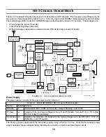
Summary of Contents for KD-34XBR2 - 34" Hdtv Fd Trinitron Wega

Page 1: ...S Training Manual Troubleshooting Information Course CTV 29 TVP 12 C29P12 Direct View Projection TVs HA 3 RA 5A Chassis Models KD 34XBR2 KDP 57XBR2 KDP 65XBR2 KDP 57XBR2 KD 34XBR2 ...

Page 2: ...rt Up 32 Protection 33 HV Adjustment 34 Testing 35 10 Communications HA 3 RA 5A Chassis 36 11 Video Process HA 3 RA 5A Chassis 40 Overall Sync Path 43 Board Replacement Repairs 44 Component Level Repair 53 DTV Tuner Processing for DTV Box Repair HA 3 RA 5A Chassis 58 12 Audio Block HA 3 Chassis 60 Signal Flow 60 Normal Signal Levels 62 13 Firmware Upgrade HA 3 RA 5A Chassis 63 14 HA 3 TV Chassis B...

Page 3: ...6 21 High Voltage Stage RA 5A Chassis 95 HV Power Supply Start Up Board level repairs 95 HV Block Description Component level repairs 95 Testing for Dark Screen 98 22 Video Process RA 5A Chassis 100 23 Board Replacement RA 5A Chassis 102 Appendix Connector Layout HA 3 Chassis i Communication HA 3 Chassis ii D Board Tests RA 5A Chassis iii Physical Video Sync Path RA 5A Chassis iv ...

Page 4: ...ts Video Off the Air Cable Video 1 4 480i NTSC format Air NTSC channels 2 69 Video 5 6 480i NTSC format or 480p 720p 1080i ATSC format Air ATSC channels 2 69 Cable NTSC channels 1 125 Technical Highlights There are three microprocessors in the Q box and the TV operations micro is on the B board They are listed in Chart 1 3 below Chart 1 3 Microprocessors in the TV Q box DTV decoder B Board AD Boar...

Page 5: ...t voltage comes from the HOT There are only a few mechanical adjustments in these TV sets and they are listed in Chart 1 4 below Chart 1 4 Mechanical Adjustments Direct View TV HA 3 chassis Projection TV RA 5A chassis G2 screen C board G2 screen controls chassis H Static control C board Static electrical focus chassis Static focus on the Flyback D board Mechanical focus lenses HV reg and shutoff p...

Page 6: ...ker Figure 2 2 Interlaced Pix Field 1 Field 2 6i Interlaced Picture consisting of alternating lines from fields 1 2 Figure 2 3 Progressive Pix 6p Progressive Scan Picture Progressive picture is for still pictures When the TV screen contains pages of still text or a still image an interlaced picture appears to jitter This is because field 2 displays the same picture as field 1 but is positioned low...

Page 7: ... C D D 1 2 3 4 5 Interlaced frame Clear Frame 3 Distorted TV frame 3 Alternate Video Audio Refer to Figure 2 1 for a sample menu page If this feature in the DTV transmission is available the user can select a second video or audio stream for a different camera angle or second language Screen Modes Menu Refer to Figure 2 6 for a sample Screen Mode menu Wide Mode you can alter the 4 3 picture you ar...

Page 8: ...sible with this TV Communications with this TV is limited to operation with the Sony CableVision cable box currently used in NYC Therefore the following information shows how to connect i LINK devices and what this TV does with an i LINK connected device Connection for Speed The IEEE 1394 allows the data transmission speed to vary between devices but the proper connection will improve communicatio...

Page 9: ...nk device itself Whenever you select that device from the list the two will operate together In this example the output of Sony camcorders is a digital DV format The DTV set is expecting an MPEG digital video format and therefore cannot display the DV format video on the screen An analog cable between the two is needed to display the camcorder video as explained in the owner s manual The TV s vide...

Page 10: ...C8801 The eight LEDs and IC9201 driver are used in i Link software loading verification not for servicing The left LED with the rear of the QI board facing you is the reset LED for the board It lights up at reset Reset occurs shortly at power ON and just before the memory stick information gets processed Fire Wire is a trademark of Apple Computer Inc i Link is a trademark of Sony IC9213 5 OSC DIVI...

Page 11: ... being received by going to the service mode and examining the transmitted PSIP information received by the TV s decoder 1 Enter the service mode Using the remote control press buttons Display 5 Volume Power On 2 Select an active DTV station using the channel up down buttons 3 Use the 2 up or 5 down buttons to locate category DTV The WSL indicates signal strength like AGC 0 strong and 255 snow 4 U...

Page 12: ...ssing time in the service mode From the service mode select category DTV Use the remote s number 3 button to change the data from 1 to 3 The following audio and video data packet processing example shown in Figure 3 2 shows the packet number going into the TV s decoder PTS and what packet has been successfully processed PCR At the right is the decoder processing time is given in ms The greater the...

Page 13: ...GES 200V ON OFF RY6501 Q BD LOWER VOLTAGES H V SYNC RGB VIDEO A VIDEO B VIDEO IN U HB BD s YOKE Q BOX TUNER A TUNER B HV HI SCAN VIDEO HD VD RGB VD HD A BD F BD D BD C BD 43TVP12 1359 B BD SEC P S FIGURE 4 1 HA 3 CHASSIS OVERALL BLOCK STANDBY P S SPLITTER ISOLATOR Power Supply The power supply consists of three parts as shown in Chart 4 1 Chart 4 1 Model KD34XBR2 HA 3 Chassis Power Supplies Name B...

Page 14: ...the component video input into RGB for the CRT cathodes and uses the sync input to lock the 60 Hz vertical oscillator and 33 75kHz horizontal oscillator High Resolution Input Video inputs 5 and 6 are for Y Pr and Pb component video signal types only They can be standard 480i or high resolution 480p 720p or 1080i formats The standard resolution signal must be switched into the DRC circuit using the...

Page 15: ... for the destination of output voltages IC6002 REG Q2006 PROT LATCH Q6530 Q6532 IC003 RESET IC001 MAIN MICRO M306V2MF STBY P S T6703 D6702 7 8 69 44 45 50 46 32 1 3 1 1 2 5 7 FRONT PANEL PWR HA BD OVP OCP STBY 5V STBY 15V SOURCE STBY 5V AC RELAY D2007 D2008 STBY 7V SOURCE P ON HA BD TO STBY LED C2039 PRIM P S A BD SEC P S D BD F6701 6 3A RY6501 AC RELAY Q6527 SET ON S01 B OVP B OCP D6730 CN7003 CN...

Page 16: ... second half of front panel switch S01 not shown grounds the power ON input to Main Micro IC001 IC001 powers ON the TV by turning on relay driver Q6527 Q6527 grounds one end of RY6501 relay coil and momen tarily turns on Q2006 via C2039 Q2006 supplies a higher 15V to AC relay RY6501 because a relay requires more voltage to close the contacts than to hold them closed especially if the AC input volt...

Page 17: ...BD AC RELAY Q6527 R6526 O 1 CN6504 CN3170 MAIN SW B OVP CN3171 CN6506 CN6003 CN6501 PRI PRE 15V Q9V SUB 9V SUB 5V SUB 3 3V Q5V Q6 5V MAIN RELAY D BD A BD B BD D BD 50 0 1 8 30 01 13TVP12 1331 SUB 12V 46 POWER ON HA BD FIGURE 5 2 DIAGRAM 13 POWER ON 2 2 Secondary Power Supply Starting The Secondary Power Supply needs three items to operate They are listed in Chart 5 3 below Chart 5 3 Three voltages...

Page 18: ... Supply starts Q box is powered Surge relay is energized 4 Main Micro B board resets Q box The Q box has flash memories for self initialization 5 Q box acknowledges after initializing TXD and RXD communications See appendix 6 Main Micro B board starts the Secondary Power Supply Deflection and TV filaments start The Secondary power supply is started 100msec after power ON and independent of the Q b...

Page 19: ...1093C 3 1 AC RECT FROM IC6501 1 D BD R6002 0 47 OHMS R6010 R6001 R6003 R6004 R6006 C6007 VC1 VC2 VB F B OCP R6009 T6002 Q6002 Q6001 TIMER R6018 R6019 R6041 R6045 D6016 C6014 D6011 D6012 D6018 D6014 PRI PRE 15V D BD UNREG 7V SOURCE UNREG 11V SOURCE V SENSE 340VDC 3V 1 86V D6004 18V A BD R6040 Q 6 5V SOURCE 8 30 01 23TVP12 1341 32V 4 5V 10V 28V OV 32V VD VG H VS VG L FIGURE 6 1 PRIMARY POWER SUPPLY ...

Page 20: ...pin 14 The result is a VB voltage that is approximately 5V average above the reference voltage at IC6001 pin 15 This voltage supplies the top internal driver that amplifies the oscillator signal that leaves IC6001 pin 16 Secondary Power Supply Starting The Pri Pre 15V output of the primary power supply D6012 is used to enable the secondary power supply At start up the primary oscillator frequency ...

Page 21: ...Time base 2usec div Testing Chart 6 2 shows what is necessary to start and run the primary power supply and Chart 6 3 lists the voltages of the power supply s IC6001 Chart 6 2 Checks for Primary power supply operation Check Point Normal Description 1 R6006 Fusible 340Vdc P S Input voltage 2 CN6005 pin 5 15 6Vdc Pri Pre 15V Checks P S Output 3 IC6001 pin 2 Feedback voltage 1 9Vdc Feedback Voltage T...

Page 22: ...r four entry s the osc stops but can be reset by removing Vcc pin 8 voltage 15 VS Reference for high side driver 7 SS External cap determines initial start freq 200kHz in this TV 18 VD Start up voltage for VC1 low high drivers internal to the IC Max 600V 12ma Protection See Chart 6 5 below IC6001 stops operating and enters a protective stage when Chart 6 5 IC6001 enters a protective state Protecti...

Page 23: ...OSFET Start UP Although IC6501 is identical to IC6001 found in the Primary power supply IC6501 pin 18 in this supply is not connected to 340Vdc This means the VC1 voltage at pin 8 must be input externally to this stage to start IC6501 s oscillator during or after V sense at pin 1 senses voltage Refer to Figure 7 1 as you follow the following Secondary Power Supply start up sequence 1 340Vdc B is a...

Page 24: ...ondary PS if the Surge Relay does not close afterpowerON Figure 7 2 Checkpoint Locations FBT HA 3 Chassis D Board PH6503 4 CN6504 1 3 CN6501 6 Hot GND CN6501 6 PH6003 3 4 AC in IC6001 R6041 RA 5A Chassis G Board Regulation The 135V line to the Horizontal Output stage is fed back to IC6501 for regulation of the secondary power supply Error Control IC6503 and Optical Isolator PH6502 control regulati...

Page 25: ...2V 2 5V 0V 0V 4 0V 18 3V 0V 10 11 12 13 14 15 16 17 18 10V 0V 4 7V 0 V 15V 19V 19V 0V 1 5V Use the Hot ground shown in figure 1 at CN6501 pin 6 black wire Chart 7 4 Checking the Primary PS Output HA 3 Chassis RA 5A Chassis Voltage Checkpoint Voltage Checkpoint 15V 15V Bridge Rectifier D6514 15V CN6106 pins 7 9 24V CN6503 pin 7 or 8 22V CN6106 pins 4 6 135V CN5509 pin 9 135V CN6106 pin 1 200V Fusib...

Page 26: ...in Chart 8 1 Chart 1 also lists the signal that triggered the protec tion If no signal triggered the protection suspect Micro IC001 on the B board and the latch transistors Q6522 Q6530 on the D board of causing the TV shutdown Figure 8 2 shows the location of Chart 8 1 s protection signal checkpoints V LOSS POWER OFF LATCH 135V OCP IC3101 Y C CRT DRIVE Q6 5V OCP OVP IC001 MAIN MICRO A25 C25 C24 C2...

Page 27: ...le area five circuits are suspect 200V OCP HV Over current protection ABL voltage too LOW Video Output Failure Excessive HV Surge Relay did not energize Shutdown Latch Circuit failure 1 200V OCP R8043 and Q8009 monitor the current on the 200 volt line This 200 volt line supplies the High Voltage Converter stage which feeds the flyback transformer The flyback generates HV focus voltage and ABL volt...

Page 28: ...529 would turn ON This grounds the V sense voltage input to IC6501 pin 1 shutting down the secondary power supply 5 Shutdown Latch Finally an unstable standby voltage or a defect in the basic latch circuit Q6530 and Q6532 will also cause the TV to shut down without the standby light blinking This last problem is rare Testing If the TV relays turn ON but quickly turn back off with no standby light ...

Page 29: ...Bd Problem is in the HV converter stage D Bd Go to Flow Chart B No No Yes Yes D Board Q8009 FBT R8051 Front of TV CN6503 CN6505 CN6504 CN6506 CN6503 CN6505 CN6501 1 8 10 1 Pin 1 of each connector begins at this end PH6503 pin 3 The problem is in the Primary PS A Bd Surge Relay circuit D Bd or Latch circuit D Bd FIGURE 8 4 FLOW CHART A TV SHUTS OFF WITHIN 6 SECONDS OF POWER ON NO STANDBY LED DIAGNO...

Page 30: ...usually stop the 2X blinking indicating the load is at fault The 135Vdc load goes to the H Output PWM stage on the same D board and the velocity modulation coils on the V board To locate the problem monitor CN6506 pin 8 as you power ON The normal voltage here is 0Vdc If the voltage reaches 1 2V disconnect the V board and try again If the CN6506 pin 8 voltage still rises to 1 2V test the H Driver t...

Page 31: ...k Suspect the Control IC6503 and perhaps static lightning damage to PH6502 If the voltage peaks at a normal 135Vdc the problem is in the IC6505 Q6522 sensing circuit Standby light blinks four times TV Shutdown Refer to Figure 8 7 for this circuit and testing Circuit A vertical failure because of the output IC or secondary power supply both on the D board will cause the Y C Jungle CRT Drive IC3101 ...

Page 32: ...board If that does not return cathode current to within operating range so the picture appears examine each filament to see if it is lit The next step uses your scope to determine if there is drive signal to each CRT cathode Begin by looking for a positive pulse at CN9001 pins 1 3 and 5 as it enters the C board Next check for these signals at each CRT cathode R G and B If they are present examine ...

Page 33: ... will not display A V without the Q box dark screen Standby light blinks seven times TV Shutdown There are two 135V OCP monitoring circuits The first circuit will cause the Standby light to blink two times and the second will cause the light to blink seven times Both sensing and output circuits are on the D board but the indicating circuit is on the B board Circuit Refer to Figure 8 10 The second ...

Page 34: ...voltage at CN5505 pin 8 D Bd as you power ON If this voltage rises above 1 volt this 135V OCP circuit or Q3111 is responsible The 135V OCP circuit consists of R5013 Q5004 IC5007 delay cap C5006 and Q5018 on the D board not all parts shown in Figure 8 10 Q5004 IC5007 Q5018 OCP IC5002 PWM CIRCUITRY Q5003 Q5011 Q5016 200V REG IC3101 Y C CRT DRIVE CXA2150AQ IC001 MAIN MICRO M306V2MF 31 26 25 26 34 8 H...

Page 35: ...TCH ONLY D BD FIGURE 9 1 HA 3 HV BLOCK 55TVP12 1369 8 30 01 Start UP Three items listed in Chart 9 1 are necessary to start this HV power supply Chart 9 1 HV Converter Inputs Starting Name From Destination 1 200V D6515 D6517 cathode D Bd IC8002 18 199V 2 15V D6514 cathode D Bd IC8002 8 14 7V 3 AFC PLS H Out Q5030 C D Bd CN5501 pin 3 9Vp p IC8002 1 1 6V The Start sequence is as follows The Primary ...

Page 36: ...e HV oscillator IC8002 Below Normal HV After the TV is turned ON if the HV drops lower than normal the HV oscillator will stop Below normal HV is monitored by IC8001 A In normal operation a sample of the HV from D8014 causes 33V zener D8025 to conduct The HIGH that is output D8014 is turned into a LOW by inverter Q8010 Q8010 s LOW output is passed 9 4 01 Q8009 OCP Q8022 3 Q8018 DYNAMIC FOCUS AMP I...

Page 37: ...l An easy way to prove this HV protection circuit caused shutdown is to look for a momentary increase in voltage at D8027 cathode during turn ON Epoxy sealed RV8001 at IC8001 pin 9 sets the shutdown threshold When the HV is correctly set at 31 5kV the resultant voltage a test point CN5506 pin 2 is between 4 36 4 66Vdc Excessive Current Protection Excessive current drawn along the 200V line into th...

Page 38: ...5 6V at IC8002 pin 8 Look for HV Conv start voltage at IC8002 pin 1 normally 1 6Vdc but must be more than 1 3Vdc to start See Charts 9 2 and 9 3 below Chart 9 2 Converter IC8002 Voltages Pin 1 2 3 4 5 6 7 8 9 Volts 1 63 1 75 2 25 2 47 0 0 4 56 14 7 0 Pin 10 11 12 13 14 15 16 17 18 Volts 10 3 0 4 14 0 108 98 6 103 0 200 Chart 9 3 Additional Important Voltages related to IC8002 pin 1 Voltage Electri...

Page 39: ...o chassis the only communication differences between them are the final destinations of the two buses on the A and D boards 10 IC004 NVM IC001 MAIN MICRO IC8902 MID MICRO IC7205 DIG PROCESS CN002 11 11 B1 A1 2 2 11 B1 A1 13 1 RST T STBY 5V CN007 N C S DATA CLK R A10 DATA A11 CLOCK CN8801 CN8601 Q BOX B CLK DATA B BD 14 1 15 CN005 CN004 A20 2 B19 1 1 2 1 A1 B1 A11 B11 CN4402 AUDIO TUNERS CN3171 7 8...

Page 40: ...erating B levels While the TV is operating there is only periodic communications when required Waveform 10 1 shows typical Q box to Main Micro IC001 B Bd bi directional communications This waveform was taken when changing into a DTV station channel up command In the waveform sequence below notice that the Main Micro starts the communications ch 2 and the Q box micro replies afterwards ch 1 When ch...

Page 41: ...ut the Q box power S data and clock bus This data bus is bi directional with the video processor on the A board and AD board in the RA 5A projection TV chassis but unidirectional with the remainder of the ICs in the TV The clock signal comes from Main Micro IC001 Both data and clock signals are 4Vp p and are always present as long as the TV is ON This output drops to 2Vp p if the Q box power was r...

Page 42: ...mmunications bus used solely within the Q box to its OSD IC which is also within the Q box The green service mode OSD channel numbers and user functions e g volume picture come from the Main Micro IC001 on the B board IC001 communicates with the Q box for this purpose using RXD and TXD as explained above The OSD RGB output is applied to the video processor IC on the A board The white crosshatch pa...

Page 43: ...site video in standard 480i format 525 line Video 5 6 Y Pb Pr component video in 480i 480p 720p or 1080i format A general description of the video flow by board is explained for each of the four input groups 9 4 01 7TVP12 1324 ANALOG TUNERS IC3101 Y C CRT DRIVE IC002 SW Q9 Q11 Q13 MIXER IC7806 IC7807 DRC PROCESS IC8801 OSD IC001 MAIN MICRO IC7205 IC7603 DTV TUNER AND PROCESS IC9001 3 RGB OUTPUTS I...

Page 44: ...station Input A board Both the main and sub analog tuners are mounted on the A board Their composite video outputs are sent to the A V switch on the B board B board A V switch IC401 chooses the signal path for the main and sub tuners The main tuner signal may either enter the main path or be switched into the sub path The main path leaves IC205 on the B board for the QM board Q Box The sub path le...

Page 45: ...board and enter the Y C CRT Drive IC on the A board From the A board the RGB signal is applied to the CRT cathodes Q Box CN001 CN001 Sub Path Main Path A V B Bd Main Sub Sw CN005 CN004 Video Inputs CN8801 CN8601 Figure 11 3 HA 3 RA 5A Video Path Video 1 4 Input Composite video from video inputs 1 4 enter the U or front panel HB board and pass through the A V switch IC401 on the B board From there ...

Page 46: ...c is first stripped from the video on the left B board Both the main and sub sync signals input the QM board as NTSC standard but leaving is 33 75kHz to match that of the TV s horizontal oscillator frequency Normally switch IC006 on the right part of the B board just passes the 33 75kHz from the QM board s MID circuit IC6 only selects the sub path sync when the HD High Pass mode is selected from t...

Page 47: ...ure is chosen from the analog tuner or video inputs the path shown in Figure 11 6 applies Only the main signal path is used to direct the analog composite video from the rear panel U board or main tuner A board Component video Y Pb Pr with H V sync lines is sent to the QM board for conversion into a high resolution high frequency video signal to match that of the TV The OSD IC buffers the componen...

Page 48: ...aving the QM board The component video and sync pass through the B board and enter the Y C CRT Drive IC on the A board The Y C CRT Drive IC output is RGB that goes into the C board and CRT cathodes Main and Twin Mode Video Troubleshooting Because of the switching in the Twin mode we can use the Twin Mode user operation to isolate the problem to a board Use Figure 11 8 for identifying a video probl...

Page 49: ...SUB AREA B BD IC200 IC202 CHANGED PIX PROBLEM IS IN A D IC8601 MID IC8703 LARGER SAME PIX SMALLER NO YES YES YES NO PROBLEM IN A D IC7806 DRC IC7804 NO FIGURE 11 8 FLOW CHART 2 VIDEO TROUBLESHOOTING NTSC PIX DEFECT 39TVP12 1355 8 30 01 PRESS TWIN MODE MAKE LEFT PIX LARGER DO BOTH PIX HAVE THE PROBLEM SEE ADJ OVERVIEW SECTION MAKE THE RIGHT PIX LARGER WHERE IS THE DEFECT Signal Tracing to prove the...

Page 50: ... CN2003 2 CH AUDIO HA 3 A C A B 9 4 01 B BOARD PLUGS INTO CN2002 3 9 4 01 7TVP12 1324 ANALOG TUNERS IC3101 Y C CRT DRIVE IC002 SW Q9 Q11 Q13 MIXER IC7806 IC7807 DRC PROCESS IC8801 OSD IC001 MAIN MICRO IC7205 IC7603 DTV TUNER AND PROCESS IC9001 3 RGB OUTPUTS IC205 MAIN SW IC8601 IC8703 IC8902 MID PROCESS IC201 IC202 IC204 IC207 ANALOG VIDEO PROCESSING IC401 A V SW IC200 COMPONENT INTERFACE I F IC20...

Page 51: ...n A3 Output B 1Vp p NTSC Sub Component video output the B board Hi Scan Y Signal CN001 pin C15 Input B 0 7Vp p Hi Scan Pb CN001 pin C16 Input B 0 6Vp p Hi Scan Pr CN001 pin C17 Input B 0 5Vp p High Resolution Component video output Q box Menu CN001 pin C12 green Output B 0 5Vp p OSD white menu signal Waveform 11 1 shows component video leaving the B board into the Q box The main and sub signals lo...

Page 52: ... Hi Scan Pr CN001 pin C17 0 5Vp p Channel 3 Hi Scan Pb CN001 pin C16 0 6Vp p Channel 4 Hi Scan Y Signal CN001 pin C15 0 7Vp p Time base 10usec div Waveform 11 3 shows the menu signal output the Q box This menu signal is present for 1 5 minutes after the menu button is pressed The signal appears on all RGB outputs lines because the new menu is white in color Cancel the menu by pressing the menu but...

Page 53: ...art 11 5 High Definition Video Signal Path Video 5 or 6 Input DTV Air Signal Stage Board Purpose Stage Board Purpose Input U Input DTV Tuner QM DTV Reception Component Interface IC200 B Video buffer H V Sync extraction DTV Process QM Decodes one of 18 ATSC formats Input Antenna Outputs component video MID Processor QM Signal determination based upon sync freq aspect ratio change H freq change to 3...

Page 54: ...de of the screen The signal path is easy to see in Figure 11 12 and the signal path is listed in Chart 11 6 FIGURE 11 11 HD NTSC TWIN VIEW VIDEO PATH DTV TUNER PROCESSOR OSD DRC PROCESS ANALOG VIDEO PROCESS IC002 SW TUNER JUNGLE A V SW MAIN SW MID PROCESS RGB OUT TO C BD VIDEO 5 6 VIDEO 2 COMBINED PIX QM BD U BD HD BD B BD A BD COMPONENT I F VIDEO 1 3 4 NTSC NTSC HD HD HD 8 30 01 11TVP12 1327 HD P...

Page 55: ...ns locked to the main signal input MID Processor QM Selects Video 5 6 or DTV input H freq change to 33 75kHz DRC Process QM Increases the pixel number MID Processor QM Creates two pictures on the screen MID Processor QM Creates two pictures on the screen OSD QM Video buffer User Menu OSD SW IC002 B Pass through only Switch is disabled from the service mode Y C CRT Drive A Input Component Video Out...

Page 56: ... B A C Component Video Sync Menu OSD RGB to CRT cathodes 11 16 DTV Tuner QM UHF antenna Memory Stick EMI video bus DTV line audio output NEED TO TROUBLESHOOT THE ANALOG AREA OF THE SET CAN THE DEFECT STILL BE SEEN ACTIVATE THE INTERNAL VIDEO GENERATOR IS THE DEFECT SIMILAR FOR ALL INPUTS V5 V6 HIGH DEFINITION SINGLE PICTURE HAS A DEFECT DEFECTIVE CIRCUIT IS LOCATED ON B OR U BOARDS SEE CONVERGENCE...

Page 57: ...N002 IC207 MAIN YCT CXA2151Q IC202 SUB YCT CXA2103Q IC204 SUB COMB CXD2073Q IC201 SUB SW M52055FP IC205 MAIN SW M52055FP IC001 MAIN MICRO M306V2MF A7 A6 A5 A3 A2 A1 MAIN SIG TO IC7806 A D QM BD SUB SIG TO IC8601 A D QM BD Y PB PR Y PB PR MAIN SUB U BD TUNERS VIDEO 2 VIDEO 1 VIDEO 3 VIDEO 4 VIDEO 5 VIDEO 6 Y C V Y C V Y C V Y C V Y C V V A BD HB BD B BD Y C VIDEO 5 TO IC200 IC202 IC207 VIDEO 6 TO I...

Page 58: ... Swaps Twin View pictures back to original position All NTSC modes Sub Path IC204 Sub Comb Filter B Separates the luminance from the chroma Twin View IC202 Sub Y Ct B Selects input component video 5 6 or composite video from IC501 Adds Closed Caption graphics Twin View IC201 Sub Sw B Swaps Twin View pictures back to original position Twin View IC200 Component Interface B Selects NTSC sub video or ...

Page 59: ...C7807 DRC MF CXD 2095AQ IC7601 DRAM IC7602 DRAM IC7604 CONV IC7603 MPEG ST17000AQA IC8703 MID XA CXD 9509AQ A3 A2 A1 IC8601 CXA3506R A D SW A7 A6 A5 IC8803 IC8805 D A B2 A2 A3 A4 A5 B6 A6 A9 A8 A7 Y PB PR SUB FROM IC200 COMP I F Y PB PR IC7807 DRC SDA SCL IC8601 A D IC8703 MID XA MID BUSY BOX RST ANALOG Y CB CR Y PB PR OSD R OSD G OSD B HS VS MAIN FROM IC205 MAIN SW VIDEO OUTPUT CN005 CN8601 EMI B...

Page 60: ...ix with the green OSD graphics channel numbers volume etc from the main micro using Q9 Q11 and Q13 The combined OSD signal and buffered component video are applied to Y C CRT Drive IC3101 on the A board IC3101 mixes the video signal and OSD then converts the result into an RGB signal for the CRT on the C board FIGURE 11 15 VIDEO PROCESS 3 IC004 NVM IC001 MAIN MICRO M306V2MF IC9002 IC3101 Y C CRT D...

Page 61: ...nk operation Memory Stick port access Service mode green user OSD DTV video audio processing TV Protection Diagnostics DTV Tuner control Power Supply Control NTSC tuner control Q box reset Master communications 1 2 3 4 5 6 7 8 1 2 3 4 5 6 7 1 3 4 5 7 1 2 3 5 6 7 6 5V GND 5V 9V GND 33V 1 A B GRAY DIG TUNER A B 8 9 1 A B WHITE 1 11 11 11 11 BLK FBT CN7001 ALL VOLT FROM A BD CN6005 CN7402 CN8801 CN86...

Page 62: ...TO IC9202 QI BD QM BD 8 30 01 2TVP12 1319 MAIN MICRO IC001 B BD PCS IC7203 IC7204 RAM IC7201 IC7202 FLASH MEM IC7401 AUDIO DECODER STJ4600BEV The EMI bus carries the DTV digital tuner data to the MID circuit for switching into the video path See Figure 11 14 for the completion of the EMI bus IC8804 SRAM IC8902 MIDuCOM MB9489A88F IC8801OSD YGV619 IC7806 A D TLC5733AIPM IC7807 DRC MF CXD 2095AQ IC76...

Page 63: ...nd both Sel_L and Sel_R audio channels pass through the A board for processing within the S board AUDIO 1 3 4 ANALOG TUNER Q4401 2 MUTE Q4403 10 Q4405 7 IC4406 AMP W IC4404 LPF DIGITAL TUNER PROCESS IC4405 OUTPUT AMP H IC4403 AUDIO PROCESS IC401 A V SW IC4402 V F BUGGER IC4401 TRUSURROUND IC402 LEFT CH SW IC403 RIGHT CH SW AUDIO OUT AUDIO 5 AUDIO 6 MONITOR OUT AUDIO2 OUT 3 CN008 CN1200 SUB 9V L R ...

Page 64: ...nd field when the TruSurround mode is activated from the menu When acti vated Main Micro IC001 outputs a HIGH at the S Mode line that can be checked at the S board CN4401 pin 6 Chart 12 2 shows IC4401 s control voltage Chart 12 2 TruSurround IC4401 Control Voltage Audio Effect Location Voltage Off CN4401 pin 6 0Vdc OFF Simulated CN4401 pin 6 0Vdc OFF TruSurround CN4401 pin 6 5Vdc ON IC4403 Audio P...

Page 65: ...ins A board 1 4Vp p 1kHz B Board Output CN4401 pin 8 S board CN4401 pin 9 S board 1 4Vp p w 5Vdc Mid Tweeter out to Amp CN4401 pin 1 S board CN4401 pin 2 S board 0 1Vp p at half volume 0 6Vp p Max volume Low freq Output to Amp CN4401 pin 3 S board CN4401 pin 4 S board 0 018Vp p half volume 0 03Vp p Max volume Variable Fixed Output CN4401 pin 11 S board CN4401 pin 12 S board 0 22Vp p half volume 2 ...

Page 66: ... or unsuccessful upgrade completion It flashes quickly for success or stays ON for one second When unsuccessful it stays OFF for two seconds while flickering The memory stick must be removed to resume TV operation or left inserted for another attempt Technical Upgrade Operation Refer to Figure 13 1 for the technical operation IC7209 RESET IC7201 2 FLASH MEMORY IC7205 DIGITAL PROCESSOR ST20TP4CX605...

Page 67: ...isplays Memory Upgrade Mode on the screen 5 Main Micro IC001 then blanks the screen and outputs a Grant and reset XRST line to begin the upgrade After resetting the Q box microprocessors IC7205 and IC9209 the upgrade sequence starts Chart 13 2 IC001 Outputs to Q board to begin Memory Upgrade IC001 Output Location Voltage Grant CN8801 pin A1 QM Bd HIGH XRST CN7201 pin A2 QM Bd Momentary LOW 6 IC720...

Page 68: ...C7205 informs IC001 the boot up is complete 14 IC001 unblanks the CRT resuming normal TV operation Upgrade error IC7205 pulses the rear panel LED D7204 to show an error code if IC7205 discovers there is no first folder on the memory stick After loading the first folder IC7205 discovers there is no second folder for IC9209 to upgrade Memory stick is not making good contact ...

Page 69: ...Q6 5V OVP No Adjustments B Video processing and audio switching Closed caption V Chip Main Micro IC001 OSD Menu None None Transplant memory IC004 containing system and user data including analog tuner active stations see note below C RGB CRT signal amplifiers None D9010 G1 Volt limiter Adj Screen control according to the service manual Reduce vertical size to see IK line at the top Blank pix in th...

Page 70: ...2 for 31 5kV Adjust HV shutdown RV8001 according to safety related adj in the service manual F AV loss detection circuit Degaussing relay F6701 Main AC 6A None No adjustments Q Box Qi QM Bds DRC for line doubling MID for twin pictures DTV Tuner and video processing None D7803 3 9V Reg for IC7805 Write PLL QM Bd No adjustments Enter the service mode and verify the TV ID group 19 see note below D440...

Page 71: ...Contents TV s Non Volatile Memory NVM Contents B board IC004 D board IC5501 QM board IC7206 and IC8901 Active Analog Digital TV stations last channel video Deflection parameters raster parameters not video Picture parameters such as size position etc video parameters not raster User Picture Audio settings CRT Drive settings Single and Twin pix parameters User Operation settings DRC Freeze pix sett...

Page 72: ...ess the following four buttons in sequence Display 5 Volume and Power On Service Mode Categories Groups There are so many service mode adjustments possible that they are grouped into categories Within the category are items that you can adjust Finally changing the data for the item will make the adjustment See Figure 15 1 below WSL 0 Service Category Data Service Service Item Video 5 480i F A Flag...

Page 73: ...nts are found in the 2150D 1 3 D CONV and CXA2026 catagories of the service mode They should be performed in the sequence given by following the stepped procedure in the service manual In other words place the TV in the FULL picture mode form the menu and perform the adjustments starting with H Centering and finishing with Outer vertical bow Next switch to the NORMAL picture mode using the menu an...

Page 74: ... modes The different modes are accomplished by changing the video signal Procedure 1 Perform convergence or geometry adjustments in the FULL Picture Mode 2 When you finish making adjustments to that category use buttons 1 and 4 on the remote to go to the CPY item in that category CPY 1 CPY 2 or CPY 3 is the last item in the category 3 While on the CPY item Change its data from 0 to 1 button 3 4 Pr...

Page 75: ...pose IC7205 ST20TP4CX604 QM Dig Process Stores the pieces of the video pattern IC7203 4 GM71VS65163 QM D RAM Lays out the pieces map IC7603 STI7000AQA QM MPEG Decoder Inserts the map into the video chain IC8801 YGV619 QM OSD Pass through out of the bd Alternate Video 5 6 input Path used for troubleshooting only Q box video bypass is NOT fully tested Purpose All video must pass through the Q box in...

Page 76: ...isplay 5 Volume Power On 2 Select category OP buttons 2 and 5 3 Select item HDPT buttons 1 and 4 HDPT means High Definition Pass Through item 5 4 Change its data from 0 to 1 Only a 1080i video input signal will display a picture because it solely has a 33 75kHz signal frequency that matches the TV s horizontal frequency of this Hi Scan TV All the other signal inputs must be converted by the MID ci...

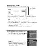
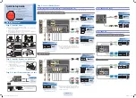
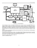
Page 77: ...74 RA 5A Chassis Board Layout ...

Page 78: ...B CR CG CB R G B R G B HV H DY V DY Hi SCAN VIDEO PROTECT Q BOX PRIM P S Power Supply The entire low voltage power supply is located on the G board The standby power supply delivers 5V to the Main Micro on the B board so it can respond to the power ON command form the remote or front panel When the TV is turned ON the Primary power supply delivers low voltages to the Q DTV decoder box the A AD and...

Page 79: ... sync lines also go to IC3006 on the A board A board Both sync and component video are sent to the A board The V H sync signals are applied to IC3006 for oscillator lock and to supply the convergence circuitry in the AD board The component video is input IC3006 and converted to RGB The RGB signal feeds the three CRT s cathodes Convergence Convergence and Flash focus are independent operations shar...

Page 80: ... IC6001 T6001 SECONDARY P S IC6002 T6004 PRIMARY P S AC INPUT OVP Q6010 D6016 IC6106 T6003 STBY P S RY6002 SURGE RELAY R6010 STANDBY 5V D6183 D6115 D6051 D6049 PS6101 2 PS6103 6 D6104 D6116 D6114 D6105 AC IN OVP ISOLATION Q6001 Q6003 PH6003 Q6104 4 5 7 6 1 9 C26 A25 C25 A26 C28 D6015 LATCH Q6105 Q6119 TH6001 R6057 STANDBY 5V SOURCE F6001 10A POWER ON RY6001 Q6120 D6001 R6099 R6041 D6105 C6036 B OC...

Page 81: ...This is a simple 60Hz step down transformer power supply with a 5V regulator IC6106 at the secondary The only unique part in this supply is the TH6001 thermistor in series with the primary winding Since T6003 is working 24 hours a day TH6003 prevents T6003 damage if the line voltage goes high for a prolonged time as commonly occurs during summer If the abnormally high AC input voltage causes T6003...

Page 82: ...he V sense 2 line into the secondary power supply is enabled The secondary power supply may now power up because its V Sense input is allowed to go HIGH All secondary PS outputs are fused except the 19V and 135V lines This power supply is connected to the D deflection and K audio boards The D board supplies 15V and 135V to the A board The destinations for the secondary power supply are listed in C...

Page 83: ...the secondary PS G board D6049 Cathode 15 6V minimum 6 Secondary PS is enabled 2 Main Micro IC001 turns on Secondary PS G board CN6101 pin 9 5Vdc 7 Secondary PS powered Secondary PS starts and runs powering TV G board CN6106 pin 9 135Vdc 8 VTIM vertical timing pulses input Main Micro IC001 Video Processor Jungle IC3006 on A board gets 9Vdc operating voltage from Primary PS and outputs VTIM pulses ...

Page 84: ...ply board will come ON and produce all voltages labeled at the connectors The schematic and measured voltages are listed in Chart 19 1 Most voltages will remain at the terminals even when the TV is shut down because these lines are completely unloaded unplugged Cold ground is either at the connectors labeled or at the heat sink of D6105 near CN6106 Chart 19 1 Unloaded Output Voltages from the G bo...

Page 85: ...terminals and ground Connect the resistor at each terminal for 10 seconds CN6104 pin 1 11V CN6104 pin 2 7V CN6106 pin 1 15V The remaining voltages will dissipate within 10 seconds C Powering up the G board power supplies after parts replacements To avoid damaging the new parts installed to the primary or secondary power supplies it is important to gradually apply power to the parts so you can dete...

Page 86: ...lator should remain at 220kHz as the input voltage increases because the regulator circuit has been disabled step 2 11 Finally test the regulating circuit by measuring the voltage across PH6005 pins 1 2 with the board powered up 0V normal 1 2V or higher means the regulating IC6107 is defective Running both the Primary and Secondary Power Supply 12 Unplug the AC and disconnect the DC voltage to the...

Page 87: ...second ary voltages in chart 2 will appear as you increase the AC input voltage The secondary PS oscillator fre quency should remain stable at approx 183kHz Note that at about 87Vac the Primary power supply will suddenly turn ON full and its 11V line will energize the Surge relay click sound This is normal so do not be startled The primary power supply will deliver these voltages from CN6104 unloa...

Page 88: ...in one of these protective states IC001 also indicates the cause by blinking the Standby LED a number of times pauses and then repeats the same count FIGURE 20 1 PROTECTION BLOCK RA 5A CHASSIS POWER OFF LATCH 15V OVP IC3006 VIDEO PROCESSOR 22V OCP AC IN OVP 135v OVP SUB 6 5V OVP OCP IC001 MAIN MICRO C24 A25 C25 C26 B19 A20 6 5 7 4 8 6X 135v OCP 9 2 7 6 CR BD 2 0X 0X 0X 3X 2X R IK G IK B IK STANDBY...

Page 89: ...D BD CN8003 CN8022 FBT CN8013 H OUT V OUT CN8016 CN3005 CN3006 CN3002 CN3008 CONV IC RA 5A G BD PH6004 SEC P S HOT GND T P CN6106 CN6101 CN6102 CN6104 AC IN PRIM P S STANDBY P S D6015 1 2 3 4 Protection Circuits After the TV enters a protective state the standby light blinks to identify one of seven problem sections The problem section not only consists of the protected circuit load but also the s...

Page 90: ...e and the TV shuts down from the excessive voltage The cause for excessive 15V is poor or no regulation in the secondary power supply or a loss of load The major load for the 15 line is the circuitry on the D board Sec P S G Bd D Board y Vertical Output IC8003 y 12V Regulator IC8004 15V CN8022 CN8013 T6003 STANDBY P S 2 3 4 1 R6119 Q6119 Q6105 4 5 C26 D6015 AC IN CN6001 R6112 100 AC RELAY RY6001 D...

Page 91: ...GND Normal 0V GBd Does the 22 Vdc line at CN6106 pin 6 rise above 18Vdc at Power On No No No No G Bd Latch is not being triggered Replace Latch Q6105 Q6119 Does TV shut down Yes Yes Yes Normal Replace PH6004 Check 135OVP GBd 135OCP DBd HP DET Q3061 ABd No load on 15V line D bd Check Vert Out IC5004 No Shutdown with no indication The problem 120VAC measures excessive 15V line above 20 Vdc 22V line ...

Page 92: ...ent on the 135V line from the Secondary Power Supply to the D C A and V boards Of all the 135 volt line loads listed the D board is the most demanding Horiz Output Q5030 and PWM Q5003 stage D board The HOT on the D board in turn supplies 200V to the RGB Video Output ICs C board 33V tuning voltage to analog tuners A board Velocity modulation coils V board VEL MOD COILS TUNER 33V IC001 MAIN MICRO IC...

Page 93: ...use the TV to enter shutdown Reinstall L6106 onto the G board If the LED still blinks 2X with the load disconnected L6106 removed the problem is on the G board sensing circuits Suspect IC6102 IC6103 and R6118 Standby light blinks three times TV Shutdown Refer to Figure 20 7 for the following 135V OVP circuit explanation and testing Circuit The 135 voltage limit is 150Vdc This limit is checked by R...

Page 94: ...9 2 2 D8001 5 6V R8015 V DY CN8009 CN8008 CN8007 8 31 01 30TVP12 1346 B19 A20 31 Standby light blinks five times Blanking Refer to Figure 20 9 for this circuit description and testing Circuit Three IK pluses are measured by Video Processor IC3006 as they return into pin 58 Each pulse corresponds to the efficiency of each CRT cathode and therefore is used to adjust the RGB gain within IC3006 to mai...

Page 95: ...n Refer to Figure 20 10 for this circuit description and testing Circuit IC001 pin 43 monitors the Sub 6 5Vdc from the Primary power supply G Bd to the Q box QM and QI boards A short or excessive voltage on the Q6 5Vdc line will cause IC001 to shut off the AC relay IC001 pin 69 goes LOW shutting down the TV and blinking the LED six times 1k BUFF IC3801 VIDEO OUT IC3701 VIDEO OUT TDA612OQ IC3006 VI...

Page 96: ...tage divider C8096 8 reduces the 1KV 31 5kHz spikes The horizontal spikes are clamped limited and shaped into rectangular pulses by zener D8026 Buffers Q8031 Q8101 apply the reshaped pulse to the horizon tal activity circuit D3011 is the first part of this circuit outputting a DC voltage to LPF C3090 R3140 The DC voltage keeps Q3037 turned ON When Q3037 is ON IC3006 pin 34 remains LOW for normal o...

Page 97: ...5011 transistors on the D board and video output ICs C board Present The D board is OK and the problem is in the sensing circuit on the A board Suspect components D3011 C3090 R3140 and Q3037 FIGURE 20 11 PROTECTION 7X INDICATION RA 5 CHASSIS IC8005 Q8027 T8003 HOT Q8030 BUFF Q8023 DRIV T8002 DRIV IC3021 REG IC3006 VIDEO PROCESSOR CXA2150 IC3005 REG 55 61 19 21 26 25 34 40 IC001 MAIN MICRO M306V2ME...

Page 98: ...uitry is defective See Testing for the procedure and location of the checkpoint connectors The HV stage can be tested for operation and level by measuring the sample of the HV at CN8016 pin 3 7 46Vdc See Figure 21 2 for the schematic and Testing for connector locations HV Block Description Component level repairs The HV Stage only has a few major blocks as shown in Figure 21 1 Q8035 HV REG HV DIST...

Page 99: ... Monitors the FBT output and stops the HV by grounding out the H Drive input Refer to Figure 21 2 for the operational description of the HV stage FIGURE 21 2 HIGH VOLTAGE STAGE RA 5 CHASSIS T8005 FBT IC8007 PROT 1 Q8028 9 ABL DRIVER Q8004 Q8016 Q8019 Q8020 H DRIVE Q8023 H OUT REG Q8027 DRIVER Q8036 Q8037 IC8008 PWM GEN 1 10 3 3 C8118 LOT T8004 1 14 12 12 1 6 2 2 4 1 HV BLK 7 VIDEO OUT B C B BD 14 ...

Page 100: ...like an enhancement N channel MOSFET Normally all leads measure infinity resistance to each other If you charge the base gate lead then connect the ohmmeter to the collector drain a resistance will appear for over an hour if the gate lead is not touched The test procedure for Q8038 is 1 Check all leads of the device with respect to each other Normal is no resistance infinity 2 Connect the negative...

Page 101: ...igh if a screen voltage is low Video blanking A B RGB cathode voltages stay abnormally high at 200Vdc No HV D A or G No HV or too low 1 Look at each CRT If there is an IK line at any CRT there is HV and deflection If there is a line missing CRT drive is missing from the A board 2 The screen control is above the speakers Turn one at a time until retrace lines appear then back off 3 Check for a samp...

Page 102: ...V or D8036 cathode Is there voltage 1 HV is OK 2 V H Deflection is OK 3 IK blanking Adj screen control one at a time to retrace then back off Did the picture come back Is there an IK line in any CRT Troubleshoot that color C board Adj screen control first Adj controls according to service manual Blanking is caused by no video output the A board Replace There is No HV Look for HV start signals Char...

Page 103: ...ideo Process or here The single CN3011 RGB output connector branches out to three CRTs simultaneously The RGB signal wires from CN3011 go directly to their corresponding CRT board In previous projection TV sets the RGB signals passed through the C boards in series The projection TV s A board has a plug in registration convergence AD board This board produces either video patterns for Flash Focus o...

Page 104: ...ath with the RGB pattern from the AD board when HIGH This also implies that a defect on the AD board can stop the normal picture and leave a blank screen The PJ TV set will still run normallywithout the AD board plugged in SUB TUNER MAIN TUNER VIDEO PROCESS P B A2 P R A3 Y A1 H S B3 V S B4 Y A5 P B A6 P R A7 H S A8 V S B8 Y A3 P B A4 P R A5 H S A6 V S B6 B9 B6 Y C15 P B C16 P R C17 H S C18 V S C19...

Page 105: ... do touch up convergence B Video processing and audio switching Closed caption V Chip Main Micro IC001 OSD Menu None None Transplant memory IC004 containing system and user data see note below chart CR CG CB RGB CRT signal amplifiers None None No adjustments D HV Regulator circuit HV Flyback H Output Reg circuit H Drive H Output V Output Two Convergence Amp packages fused Dynamic Focus Output R820...

Page 106: ...302 D2304 D2306 Surround spk protection D2602 5 Center Spk protection D2619 20 Main spk protection D2614 17 Var Fixed output protection D2624 31 No adjustments Q Box Qi QM Bds DRC for line doubling MID for twin pictures DTV Tuner and A V process None D7803 3 9V Reg for write PLL IC7805 QM Bd Enter the service mode and check the model ID category items to see if they agree with the service manual s...

Page 107: ... video Deflection parameters raster not video Convergence data Picture parameters such as size position etc video not raster User Picture Audio settings CRT Drive settings Flash Focus data Single and Twin pix parameters User Operation settings DRC Freeze pix settings Closed caption Service mode model ID Q Box CN001 CN001 Sub Path Main Path A V B Bd Main Sub Sw CN005 CN004 Video Inputs CN8801 CN860...

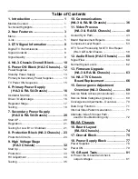
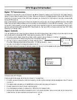
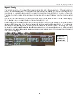
Page 108: ...APPENDIX ...
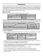
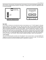
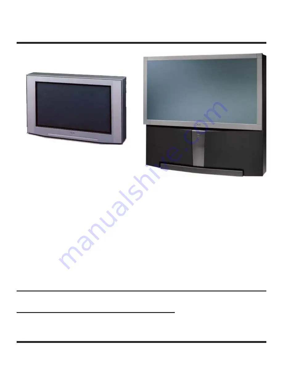
Page 109: ...CK OF THE TV 25 32 1 1 FRONT OF TV BACK OF TV QM BD A BD D BD QI BD CN2001 CN4403 CN4404 CN001 CN002 CN3173 CN5501 CN3103 CN5505 CN6003 CN6503 CN6502 OSD CN004 VIDEO TO B BD AUDIO RA 5 TO B BD CN009 VIDEO INPUT FROM B BD CN005 CN3174 CN5503 CN3171 CN6506 CN3170 CN6504 CN6001 CN6505 CN6501 SUB MAIN CN6005 HA 3 CHASSIS CONNECTOR LAYOUT 38TVP12 1354 CN2002 CN2003 2 CH AUDIO HA 3 A C A B 9 5 01 B BOAR...

Page 110: ...2 B19 1 1 2 1 A1 B1 A11 B11 CN4402 AUDIO TUNERS CN3171 7 8 2 1 CN6506 CN3173 CN5501 CONV D FOCUS D BD A BD CN2003 HA 3 CHASSIS COMMUNICATION 52TVP12 1364 9 5 01 CLOCK DATA 4Vp p PRESENT WHEN TV IS ON A25 B25 7 8 IC5001 NVM S COMMUNICATIONS DATA CLJ CN005 A10 A11 CN007 1 13 CN4402 15 14 CN6506 2 1 CN5501 8 7 CN2003 A2 B1 B COMMUNICATIONS DATA CLJ CN2003 A10 B1 B2 A11 B11 CONN DESC PATH A2 MID BUSY ...

Page 111: ... voltage matches that of the load The DVM used was a Fluke 8050A set to 200k ohm range Your ohmmeter will show different readings but they will be proportional The DVM leads were reversed so the voltage from the DVM was applied to the 22 and 15 volt pins of CN8013 pins 1 and 4 By maintaining the correct polarity premature parts failures can be avoided See Chart 24 1 Chart 24 1 D Board Excessive Cu...

Page 112: ...19 SUB TUNER VIDEO MAIN TUNER VIDEO V1 A1 Y1 A2 C1 A3 Y A15 PB A16 PR A17 VIDEO 1 VIDEO 6 INPUTS R 2 G 3 B 5 CN3011 PINS CN001 CN002 CN3020 CN3022 CN003 CN7001 CN7402 CN8801 CN8601 RGB C BOARDS U BD B BD Q BOX A BD B9 B6 CN005 CN004 SUB MAIN PHYSICAL VIDEO SYNC PATH RA 5A CHASSIS 50TVP12 1363 9 7 01 A1 B1 B11 A11 A1 C1 A25 C31 A32 C32 B1 A1 B11 A11 B1 A11 B11 A1 B1 A11 B11 A1 A1 C1 A1 B1 B25 32 1 ...

Page 113: ...of Sony Electronics Inc 1 Sony Drive Park Ridge New Jersey 07656 C29P12901 Printed in U S A Sony Service Company A Division of Sony Electronics Inc 2001 All Rights Reserved Printed in U S A S is a trademark of Sony Electronics 09 07 01 ...

Reviews: