background image

A-1

KDL-32EX600/40EX600/46EX600

KDL-32EX600/40EX600/46EX600

Sony Corporation

Sony Technology Center

Technical Services

Service Publication Department

9-883-848-51

English

2010DJ74WEB-1

Printed in USA

© 2010.4

is a trademark of Sony Electronics

Reproduction in whole or part without written permission is prohibited. All rights reserved

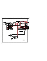
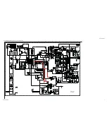
APPENDIX A:  ENCRYPTION KEY COMPONENTS


Encryption key components developed by Sony Corporation contain con

fi

 dential 

information, and shall be handled under the non-disclosure obligations provided in the 
applicable agreement with Sony Corporation (and/or its subsidiary). 


As part of this agreement speci

fi

 c instructions must be adhered to whenever a Circuit 

Board containing encryption key components is repaired and/or replaced pursuant to the 
following:

1)  In the service manual the Circuit Board(s) containing encryption key components 

shall be identi

fi

 ed with a red outline and a  .

2)  Only repair boards or components listed in the service manual shall be utilized for 

replacement and/or repair.

3)  Disassembly, decryption, or reverse-engineering component(s) is strictly prohibited.

4)  Any board in which the Servicer replaces an encryption key component must be 

placed back into the set it orignally came from and the replaced defective component 
MUST BE DESTROYED. Boards cannot be swapped.

5)  If a Circuit Board identi

fi

 ed with a red outline and a   in the service manual is deemed 

to be defective:

a)  and if a core charge is imposed and is covered under the product warranty, the 

defective un-repaired or modi

fi

 ed board MUST BE RETURNED to Sony.

b)  and if the core charge is NOT covered under the product warranty, the defective 

un-repaired or modi

fi

 ed board MUST BE DESTROYED.

5)  If a unit is destroyed (such as 

fi

 eld scrap), the Circuit Board identi

fi

 ed with a 

red outline and a   in the service manual MUST BE DESTROYED. 

Summary of Contents for KDL-32EX600 - 32" Class Bravia Ex600 Hdtv

Page 1: ...00 RM YD034 MX LATIN AMERICA KDL 40EX600 RM YD034 US CND KDL 40EX600 RM YD034 MX LATIN AMERICA KDL 46EX600 RM YD034 US CND KDL 46EX600 RM YD034 MX LATIN AMERICA LEVEL 3 CONFIDENTIAL HISTORY INFORMATION FOR THE FOLLOWING MANUAL ORIGINAL MANUAL ISSUE DATE 4 2010 REVISION DATE SUBJECT 4 2010 No revisions or updates are applicable at this time ...

Page 2: ...matic Diagram 8 of 20 16 A Board Schematic Diagram 9 of 20 17 A Board Schematic Diagram 10 of 20 18 A Board Schematic Diagram 11 of 20 19 A Board Schematic Diagram 12 of 20 20 A Board Schematic Diagram 13 of 20 21 A Board Schematic Diagram 14 of 20 22 A Board Schematic Diagram 15 of 20 23 A Board Schematic Diagram 16 of 20 24 A Board Schematic Diagram 17 of 20 25 A Board Schematic Diagram 18 of 20...

Page 3: ...D panel must be secured using the 4 mounting holes on the rear cover To avoid damaging the LCD panel do not press on the panel or frame edge to avoid the risk of electric shock do not scratch or press on the panel with any sharp objects do not leave the module in high temperatures or in areas of high humidity for an extended period of time do not expose the LCD panel to direct sunlight avoid conta...

Page 4: ...lowing part numbers Due to the higher melting point of Lead Free Solder the soldering iron tip temperature needs to be set to 370 degrees centigrade This requires soldering equipment capable of accurate temperature control coupled with a good heat recovery characteristics For more information on the use of Lead Free Solder please refer to http www sony training com r e b m u n t r a P r e t e m a ...

Page 5: ...A 500 microamperes Leakage current can be measured by any one of three methods 1 A commercial leakage tester such as the Simpson 229 or RCA WT 540A Follow the manufacturers instructions to use these instructions 2 A battery operated AC milliampmeter The Data Precision 245 digital multimeter is suitable for this job 3 Measuring the voltage drop across a resistor by means of a VOM or battery operate...

Page 6: ...fidential information Specific instructions must be adhered to whenever these components are repaired and or replaced See Appendix A Encryption Key Components in the back of this manual All capacitors are in μF unless otherwise noted pF μμF 50WV or less are not indicated except for electrolytics and tantalums All electrolytics are in 50V unless otherwise specified All resistors are in ohms k 1000 ...

Page 7: ...mmon Cathode Cathode Common Cathode Cathode Common Common Common Common Cathode Anode Base Emitter Collector Base Emitter Collector Drain Gate Gate Drain Device Printed symbol Terminal name Circuit Terminal name of semiconductors in silk screen printed circuit Anode Anode Anode Cathode Anode Anode Cathode Transistor FET Transistor FET Emitter Collector Base Transistor Source Gate Drain Cathode Ano...

Page 8: ...8 KDL 32EX600 40EX600 46EX600 KDL 32EX600 40EX600 46EX600 1 3 BLOCK DIAGRAMS ...

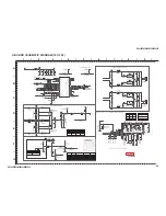
Page 9: ...L 32EX600 40EX600 46EX600 KDL 32EX600 40EX600 46EX600 1 2 3 4 5 6 7 8 9 A B C D E F G 1 4 SCHEMATICS AND SUPPORTING INFORMATION A 1 20 DC CONVERTER I 1 857 593 11 AZ1K A P1 A BOARD SCHEMATIC DIAGRAM 1 OF 20 ...

Page 10: ...10 KDL 32EX600 40EX600 46EX600 KDL 32EX600 40EX600 46EX600 1 2 3 4 5 6 7 8 9 A B C D E F G A BOARD SCHEMATIC DIAGRAM 2 OF 20 A 2 20 DC CONVERTER II 1 857 593 11 AZ1K A P2 ...

Page 11: ...11 KDL 32EX600 40EX600 46EX600 KDL 32EX600 40EX600 46EX600 1 2 3 4 5 6 7 8 9 A B C D E F G A BOARD SCHEMATIC DIAGRAM 3 OF 20 A 3 20 DC CONVERTER III 1 857 593 11 AZ1K A P3 ...

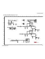
Page 12: ...12 KDL 32EX600 40EX600 46EX600 KDL 32EX600 40EX600 46EX600 1 2 3 4 5 6 7 8 9 A B C D E F G A BOARD SCHEMATIC DIAGRAM 4 OF 20 A 4 20 INPUT ANALOG VIDEO 1 857 593 11 AZ1K A P4 ...

Page 13: ...13 KDL 32EX600 40EX600 46EX600 KDL 32EX600 40EX600 46EX600 1 2 3 4 5 6 7 8 9 A B C D E F G A BOARD SCHEMATIC DIAGRAM 5 OF 20 A 5 20 INPUT D SUB 1 857 593 11 AZ1K A P5 ...

Page 14: ...14 KDL 32EX600 40EX600 46EX600 KDL 32EX600 40EX600 46EX600 1 2 3 4 5 6 7 8 9 A B C D E F G A BOARD SCHEMATIC DIAGRAM 6 OF 20 A 6 20 INPUT HDMI I 1 857 593 11 AZ1K A P6 ...

Page 15: ...15 KDL 32EX600 40EX600 46EX600 KDL 32EX600 40EX600 46EX600 1 2 3 4 5 6 7 8 9 A B C D E F G A BOARD SCHEMATIC DIAGRAM 7 OF 20 A 7 20 INPUT HDMI II 1 857 593 11 AZ1K A P7 ...

Page 16: ...16 KDL 32EX600 40EX600 46EX600 KDL 32EX600 40EX600 46EX600 1 2 3 4 5 6 7 8 9 A B C D E F G A BOARD SCHEMATIC DIAGRAM 8 OF 20 A 8 20 INPUT HDMI SW 1 857 593 11 AZ1K A P8 ...

Page 17: ...17 KDL 32EX600 40EX600 46EX600 KDL 32EX600 40EX600 46EX600 1 2 3 4 5 6 7 8 9 A B C D E F G A BOARD SCHEMATIC DIAGRAM 9 OF 20 A 9 20 TUNER 1 857 593 11 AZ1K A P9 ...

Page 18: ...18 KDL 32EX600 40EX600 46EX600 KDL 32EX600 40EX600 46EX600 1 2 3 4 5 6 7 8 9 A B C D E F G A BOARD SCHEMATIC DIAGRAM 10 OF 20 A 10 20 AUDIO IN 1 857 593 11 AZ1K A P10 ...

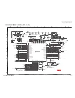
Page 19: ...19 KDL 32EX600 40EX600 46EX600 KDL 32EX600 40EX600 46EX600 1 2 3 4 5 6 7 8 9 A B C D E F G A BOARD SCHEMATIC DIAGRAM 11 OF 20 A 11 20 MT5388 INPUT 1 857 593 11 AZ1K A P11 ...

Page 20: ...20 KDL 32EX600 40EX600 46EX600 KDL 32EX600 40EX600 46EX600 1 2 3 4 5 6 7 8 9 A B C D E F G A BOARD SCHEMATIC DIAGRAM 12 OF 20 A 12 20 MT5388 DDR II 1 857 593 11 AZ1K A P12 ...

Page 21: ...21 KDL 32EX600 40EX600 46EX600 KDL 32EX600 40EX600 46EX600 1 2 3 4 5 6 7 8 9 A B C D E F G A BOARD SCHEMATIC DIAGRAM 13 OF 20 A 13 20 MT5388 LVDS 1 857 593 11 AZ1K A P13 ...

Page 22: ...22 KDL 32EX600 40EX600 46EX600 KDL 32EX600 40EX600 46EX600 1 2 3 4 5 6 7 8 9 A B C D E F G A BOARD SCHEMATIC DIAGRAM 14 OF 20 A 14 20 MT5388 PERIPHERAL FLASH 1 857 593 11 AZ1K A P14 ...

Page 23: ...23 KDL 32EX600 40EX600 46EX600 KDL 32EX600 40EX600 46EX600 1 2 3 4 5 6 7 8 9 A B C D E F G A BOARD SCHEMATIC DIAGRAM 15 OF 20 A 15 20 MT5388 INPUT 1 857 593 11 AZ1K A P15 ...

Page 24: ...24 KDL 32EX600 40EX600 46EX600 KDL 32EX600 40EX600 46EX600 1 2 3 4 5 6 7 8 9 A B C D E F G A BOARD SCHEMATIC DIAGRAM 16 OF 20 A 16 20 AUDIO AMP 1 857 593 11 AZ1K A P16 ...

Page 25: ...25 KDL 32EX600 40EX600 46EX600 KDL 32EX600 40EX600 46EX600 1 2 3 4 5 6 7 8 9 A B C D E F G A BOARD SCHEMATIC DIAGRAM 17 OF 20 A 17 20 AUDIO SPDIF LINEOUT 1 857 593 11 AZ1K A P17 ...

Page 26: ...26 KDL 32EX600 40EX600 46EX600 KDL 32EX600 40EX600 46EX600 1 2 3 4 5 6 7 8 9 A B C D E F G A BOARD SCHEMATIC DIAGRAM 18 OF 20 A 18 20 IR USB KEYPAD 1 857 593 11 AZ1K A P18 ...

Page 27: ...27 KDL 32EX600 40EX600 46EX600 KDL 32EX600 40EX600 46EX600 1 2 3 4 5 6 7 8 9 A B C D E F G A BOARD SCHEMATIC DIAGRAM 19 OF 20 A 19 20 MCU I 1 857 593 11 AZ1K A P19 ...

Page 28: ...28 KDL 32EX600 40EX600 46EX600 KDL 32EX600 40EX600 46EX600 1 2 3 4 5 6 7 8 9 A B C D E F G A BOARD SCHEMATIC DIAGRAM 20 OF 20 A 20 20 MCU II 1 857 593 11 AZ1K A P20 ...

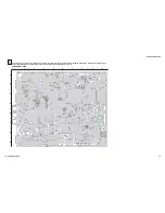
Page 29: ...2 C337 CN950 C298 C4157 C4155 C4156 CN4152 R4166 R4161 R4201 SW706 SW701 SW702 R285 R267 C271 C270 C203 Q314 R204 R201 R206 IC311 IC309 C330 C340 C336 R3356 L292 L413 L412 L411 L410 L422 L419 L418 L417 L416 L415 L414 L423 L405 L404 L403 L402 L401 L400 L421 L420 L409 L408 L407 L406 L234 Q8306 R4178 R4177 R4195 R4203 R4183 C702 IC266 C333 R3341 R 3345 D904 D903 R953 R951 C950 C951 R281 C264 R280 C83...

Page 30: ...1 C8206 C8196 C8194 C220 Q206 C522 C541 C531 C523 C536 R275 R274 C501 C4508 C4465 C4458 C4453 C287 C4451 C509 C4457 C4454 C4452 C4466 C4463 C4456 TP4024 C4472 C4471 C8219 D4309 D4308 C4486 C4503 C4504 C4488 C4485 L210 D4310 R8156 C504 TP4301 C543 C546 C544 C521 C507 C4464 C4460 R501 C4512 C4482 C4513 C4467 C4461 C4455 C4481 C4474 L290 L288 C4500 C4496 C4497 C4511 C4502 C4501 L209 L276 C4521 C4489 ...

Page 31: ...0LS0 Q6817 V 0 5 A 5 0 0 0 8 6 F S INK0001AC Q6820 1 10W RN CP R6866 470 PWM_DIMMER 001 13H 002 15D 2SC5950G0LS0 Q6816 1 10W RN CP R6858 5 10k 1 10W RN CP R6867 2 2k 1 10W RN CP R6876 1k 25V C6824 X7R 1608 0 22 1 10W RN CP 5 R6859 47 S INK0001AC Q6818 1 10W RN CP R6869 1k R6850 0 47 2W RS 1 10W RN CP R6877 100 JL6804 JL6801 JL6803 JL6802 JL6806 JL6805 JL6807 GND JL6808 1 10W RN CP 220k R6844 0 5 U...

Page 32: ...PRI_VCC1 001 10H AC_DET 001 12H MAIN_UNREG_1 001 11B 12V 001 17A 001 17E MAZ8150G0LS0 D6404 MA2J1110GLS0 D6405 RN CP R6412 1k 1 10W MA2J1110GLS0 D6403 1 10W RN CP 10k R6406 1 10W RN CP 1k R6401 1k R6402 RT1N14BC TP 1 Q6401 Mount Mecha 329654901 A6151 D6151 D6152 MAIN_UNREG_2 001 11B 1608 50V 0 1 X7R C6170 2012 50V 1 X6S C6175 35V 470 C6153 RB050LA 40TR D6154 CHIP 0 R6177 1 16W RN CP 0 5 150k R6174...

Page 33: ...0 3 R 6 1 1 8 D 6 5 0 5 R 6 1 1 9 R 6 5 0 2 R 6 5 0 3 R 6 3 1 0 R 6 3 1 1 R 6 5 0 5 R 6 3 1 2 R 6 5 0 6 R 6 3 1 5 R 6 5 1 0 R 6 5 1 1 R 6 5 1 2 R 6 5 1 4 R 6 5 1 5 R 6 5 1 6 R 6 5 1 7 R 6 5 1 8 C 6 1 5 9 R 6 5 1 9 R 6 5 2 0 R 6 5 2 1 R 6 5 2 2 C 6 1 6 3 R 6 5 2 5 R 6 5 2 6 C 6 1 6 7 R 6 5 3 2 R 6 5 3 4 R 6 5 4 3 C 6 0 0 2 C 6 2 0 7 C 6 2 0 8 C 6 2 0 9 C 6 0 1 6 C 6 4 0 1 C 6 2 1 1 Q 6 4 0 1 C 6 2 ...

Page 34: ... 002 15D DSC500100L Q6824 1 10W RN CP 5 100k R6885 1 10W RN CP 5 22k R6886 DRC5144E0L Q6825 BL_ON 001 13H 001 14B 002 15D GND_4 12V 001 13H 001 17A 001 17E 002 13E R6812 470 50V CH C6837 1000p 50V CH C6838 1000p 16V B C6839 0 1 1 10W RN CP 4 7k R6888 1 10W RN CP 470 R6887 1 10W RN CP 0 5 10k R6898 1 10W RN CP R6895 1k 220k R6890 1 10W RN CP RN CP 220k R6891 1 10W 220k R6892 220k R6893 1 10W RN CP ...

Page 35: ...72 1608 50V X7R C6176 2200p 4 7 R6178 4 7 R6179 35V 470 C6154 3216 50V 4 7 X7R C6155 9 0 1 1 1 2 1 3 1 4 1 8 7 6 5 4 3 2 1 IC6150 LV5768M DA2J10100L D6156 16V 470 C6177 16V 470 C6178 16V 470 C6179 1W RS R6165 470 S ATP201 V TL H Q6154 S ATP212 S TL H Q6155 3216 25V 4 7 X7R C6181 1 10W RN CP R6161 180k RN CP 180k R6162 1 10W RN CP 470 R6169 1 10W 0 5 RN CP 39k R6168 1 10W 0 5 2012 50V B C6171 0 1 1...

Page 36: ... 1 J L 6 8 0 2 J L 6 8 0 3 J L 6 8 0 4 J L 6 8 0 5 C 6 0 0 2 J L 6 8 0 6 C 6 0 0 3 J L 6 8 0 7 J L 6 8 0 8 C 6 0 0 5 J L 6 8 0 9 C 6 0 0 7 C 6 0 0 8 C 6 0 0 9 J L 6 8 1 0 J L 6 8 1 1 J L 6 8 1 2 J L 6 8 1 3 J L 6 8 1 4 C 6 2 0 4 P H 6 1 0 0 J L 6 8 1 5 C 6 2 0 5 C 6 0 1 1 J L 6 8 1 6 C 6 2 0 6 C 6 0 1 2 J L 6 8 1 7 C 6 2 0 7 J L 6 8 1 8 C 6 0 1 4 C 6 2 0 8 J L 6 8 1 9 C 6 2 0 9 C A 6 0 0 1 C 6 0 1...

Page 37: ... 1 9 R 2 9 R 1 C 33 9 2 1 3 R91 7 2 6 2 1 9 R TP2 9 C 1 0 2 9 C 1 2 1 9 C 1 1 6 1 9 C 9 1 L9 2 0 1 1 9 C 3 1 4 1 1 9 C 1 9 C 05 8 0 1 9 C 1 9 C 07 7 0 1 9 R R9106 3 P T L9101 1 9 C 5 1 R9105 C9106 D9112 D 9113 2 1 1 9 R 9 R 1 1 1 C9110 D9107 TP4 C9103 C9109 D9108 0 1 9 L 3 1 1 1 9 D 9 0 1 9 D TP5 TP6 TP7 9 C 1 7 1 CN9101 1 0 1 9 C 2 0 1 9 C C9111 R9110 C9112 R9109 6 0 1 9 D 0 1 1 9 D H2 IR LED 1 8...

Page 38: ...cuit Board s containing encryption key components shall be identified with a red outline and a 2 Only repair boards or components listed in the service manual shall be utilized for replacement and or repair 3 Disassembly decryption or reverse engineering component s is strictly prohibited 4 Any board in which the Servicer replaces an encryption key component must be placed back into the set it ori...

Reviews: