35
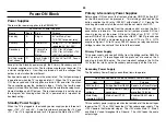
Secondary Power Supply
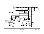
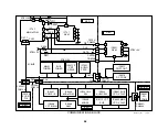
The Primary and Secondary power supplies are similar because they use
the same IC and driver/output stage. They differ in start up and output
voltages.
Start UP
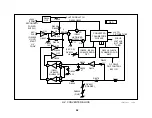
Although IC6501 is identical to IC6001 in the Primary power supply, IC6501/
pin 18 in this supply is not connected to 340Vdc. This makes VC1 at pin
8 the primary source of power to start this IC after pin 1 senses voltage.
The start up sequence is listed as follows:
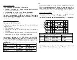
1. 340Vdc (B+) is applied to this stage from bridge rectifier D6530.
2. Pri Pre 15V voltage from the Primary power supply is applied to IC6501/
pin 8. It must be at least 15.6Vdc to enable IC6501’s internal oscilla-
tor.
3. Main Relay signal from Main uCom IC701/pin 72 (HIGH at CN6501/
pin 5) turns ON Q6531, PH6503 and Q6528. Q6528 turns OFF Q6503,
enabling voltage to appear at IC6501/pin 1.
4. R6646 and R6513 deliver at least 1.3Vdc to IC6501/pin 1.
5. IC6501 turns ON using voltage from pin 8 to run the oscillator.
6. An internal diode connected between pin 8 and 10 supplies voltage to
VC2.
7. Oscillator pulses from VC2 pass blocking diode D6502 to make a
(“pump up”) voltage for the internal predriver amplifier stage.
8. Oscillator signal outputs IC6501/pins 12 and 16.
In summary, these items are necessary to run the Secondary Supply:
Three Items needed to run the Secondary Power Supply
Item
From
Purpose
340Vdc (B+)
(CN6501/pin 1)
Bridge Rectifier D6530
Powers the Driver/Output
Pri Pre 15V
voltage
(CN6501/pin 5)
Primary Power Supply
secondary
Starts the oscillator when
more than 15.6Vdc.
Main Relay
(normally HIGH
at CN6504/pin 2)
Main uCom IC701
Enables IC6501 when
HIGH
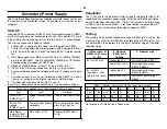
Regulation
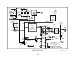
The +135V line to the Horizontal Output stage is fed back to IC6501 for
regulation of the secondary power supply. Error Control IC6503 and Optical
Isolator PH6502 control regulation. If the +135V output rises, the voltage
at IC6501/pin 2 lowers to correct. A reduced voltage increases the oscil-
lator frequency and decreases the output voltages of T6501.
Testing
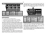
The typical error correction feedback voltage at IC6501/pin 2 is 2Vdc. By
measuring the +135V B+ at R6598 and the feedback at IC6501/pin 2, you
can determine if the problem is in the basic oscillator stage or the error
regulator stage.
1. Measure B+ at
R6598 (0.27 ohms
at 1W)
2. Measure
IC6501/pin 2
Voltage
3. Problem area
Higher than 2V
Oscillator stage IC6501
B+ is LOW or 0V
Lower than 2Vdc
Error regulating stage
IC6503/PH6502
Higher than 2V
Error regulating stage
IC6503/PH6502
B+ is HIGH
(shutdown
Stby
light blinks 3 times)
Lower than 2Vdc
Oscillator/Driver Stage
IC6501
IC
V l
(P
ON Vid
i
D k
)
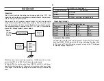
IC6501 Voltages (Power ON, Video 1 input, Dark screen)
1. 2. 3. 4. 5. 6. 7. 8. 9.
2.5V
1.8V
2.2V
2.5V
0V
0V
4.0V
18.3V
0V
10. 11. 12. 13. 14. 15. 16. 17. 18.
10V
0V
4.7V
0 V
-15V
-19V
-19V
0V
1.5V
Hot ground is at CN6501/pin 6 (black wire).
Summary of Contents for KV-32XBR400
Page 1: ......
Page 5: ...1 NOTES ...
Page 12: ...8 NOTES ...
Page 14: ...10 NOTES ...
Page 83: ...APPENDIX ...


