background image

4

Analog 

Mfg.

Model

Ch 1-99 Digital TV

Ch 1-125 Cable DTV *

Ch 2-69 Analog TV

Small dish Satellite

RF(Ch 3/4)

Comp Video

S Video

Y, Pr, Pb

RGB,H,V **

Format (# Horiz lines)

L & R

Optical

Coax

IEEE 1394

RCA

DTC-100

X

X

X

X

X

X

X

VGA 1080i/540p

X

X

Panasonic TU-HDST50

X

X

?

X

X

X

720p

X

X

TU-HDS20

X

X

X

X

?

X

X

X

BNC

?

X

X

Pioneer

SH-DO7

X

?

X

1080i ***

X

X

X

SH-D505

X

X

?

X

X

X

BNC

1080i/

X

X

X

720p/480p

Mitsubishi SR-HD400

X

X

X

X

X

X

X

X

?

X

X

SR-HD500

X

X

X

X

X

X

X

X

?

X

X

Sony

DTR-HD1

X

X

X

phono

1080i

X

X

SAT-HD100

X

X

X

X

X

X

VGA 1080i/480p

X

X

Sharp

TUDTV1000

X

X

X

X

X

VGA/ 1080i/480p

X

X

X

BNC

Proscan

PSHD105

X

?

?

X

X

X

X

VGA 1080i/540p

X

X

Samsung SIRT100

X

?

?

X

X

X

X

?

1080i/480p

X

X

*  DTV must be 8VSB modulation (like terrestrial ATSC DTV transmissions)

X = Yes

** VGA = computer monitor jack (15 pin D type) 

? = insufficient information

    BNC = BNC connectors, one for each of the signals

blank = No

*** Connection to Pioneer model PRO-700HD TV only.

Digital 

Audio Output

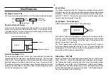
DTV Set Top Converter Boxes (as of July, 2000)

Standard Resolution

High Resolution

Video Output

RF Inputs

Summary of Contents for KV-32XBR400

Page 1: ......

Page 2: ...S Training Manual Circuit Description and Troubleshooting Course DTV 02 Direct View Television DX 1A Chassis Models KV 32XBR400 KV 36XBR400 ...

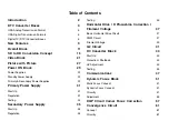
Page 3: ...ly 31 Start Up 31 Regulation 31 Testing 33 Secondary Power Supply 35 Start Up 35 Regulation 35 Table of Contents Testing 35 Horizontal Drive H Pincushion Correction Filament Voltage 37 Basic Horizontal Drive Circuit 37 PMW Circuit 37 Filament Voltage 39 G2 Circuit 41 HV Converter Block 43 Start Up 43 Protection Shutdown 43 HV Adjustment 43 Testing 45 Communications 47 Dynamic Focus Block 51 Static...

Page 4: ... Vertical Process 67 Audio Block Diagram 71 Features 71 Signal Path 71 Self Diagnostic Block 73 Self Diagnostic Circuit 75 Appendix Service Mode Display i Digital Satellite System Converter Box ii DTV Set Top Box iii IEEE 1394 iv DX 1A Chassis Assembly vii Board Replacement viii HV Adj check Bulletin 492 ixi ...

Page 5: ...1 NOTES ...

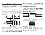
Page 6: ...rder Video 5 6 Stereo Jacks Component video Standard Resolution 480i 480p or High Resolution 1080i format DTV Satellite or Cable Converter box Control S Sony Audio Equipment Circuitry Information The power consumption and self diagnostics remain the same as other Sony TVs This set s change to high resolution video results in circuitry changes to the video processing horizontal frequency fixed at 3...

Page 7: ...tional Television Standards Committee TV trans mission standard 525 horizontal lines are transmitted but only about 480 lines are visible This is because the vertical blanking area above the picture is not seen and the picture is normally over scanned larger than the TV screen Therefore the TV resolution is said to be 480 horizon tal lines instead of the transmitted 525 lines USA Analog Transmissi...

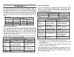
Page 8: ...X X X SR HD500 X X X X X X X X X X Sony DTR HD1 X X X phono 1080i X X SAT HD100 X X X X X X VGA 1080i 480p X X Sharp TUDTV1000 X X X X X VGA 1080i 480p X X X BNC Proscan PSHD105 X X X X X VGA 1080i 540p X X Samsung SIRT100 X X X X X 1080i 480p X X DTV must be 8VSB modulation like terrestrial ATSC DTV transmissions X Yes VGA computer monitor jack 15 pin D type insufficient information BNC BNC conne...

Page 9: ...gital transmission formats approved by the ATSC Ad vanced Television Standards Committee in the USA The first six offer HD high definition resolution signals in a 16x9 aspect ratio The remain ing 12 formats are SD standard definition signals in progressive p or interlaced i scan Note that the 480p signal can be a 4 3 or 16 9 aspect ratio transmission 18 Digital Transmission Formats Resolution Aspe...

Page 10: ...er boxes can receive digital satellite signals This combina tion of DTV and satellite decoding in one box is feasible because the decoding circuitry is similar It is uncertain if these converter boxes can decode the new satellite high definition DTV signals Video Outputs The converter boxes output standard resolution and high resolution sig nals All the boxes can down convert a 1080 720 or 480 lin...

Page 11: ...venience or high speed Customarily both video and audio is sent on this 4 wire cable More about the IEEE 1394 format is found in the appendix of this book Dolby is a registered trademark of Dolby laboratories Fire Wire is a trademark of Apple Computer Inc i LINK is a trademark of Sony ...

Page 12: ...8 NOTES ...

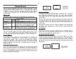
Page 13: ...ntering the owner s four number password enables viewing of the blocked programs The owner s password can be cleared with the master pass word 4357 HELP The owner s password can also be reset from the service mode by pressing 8 then enter Set Up Menu 16 9 Enhanced A 480p input signal can be in 4 3 or 16 9 video format The wide 16 9 video format produces a picture on a 4 3 picture tube that is too ...

Page 14: ...10 NOTES ...

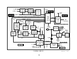
Page 15: ...ertical Pincushion Correction As the TV screen becomes larger the yoke can not perfectly control the beam at the screen perimeter An additional coil on the top and bottom of the CRT neck assembly is fed V Pin correction signal from IC201 and IC5514 The additional coil eliminates any minor inward outward bow at the top and bottom of the picture Horizontal Deflection The higher 33 75kHz horizontal f...

Page 16: ...GB OUT IC8002 HV CONV PRIMARY P S IC701 MAIN uCOM STANDBY 135V VTIM E W CY IN DY VPIN VID SYNC 480i AFC CRT FILAMENT 200V C BD COIL ON CRT NECK V DY FOCUS VTIM IC5513 CRT CATHODES PRE 15V SYNC B BD 200V H DY POWER ON 200V HOT MAIN 9V 480p 1080i 5V 7V C BD D BD A BD A BD IK MAIN VOLTAGES 12V 9V 5V 24V 15V SET VOLTAGES 9V 5V 3 3V G2 48DTV02 1273 STBY 15V 100V HV SECONDARY P S IC707 NVM IC5501 NVM D ...

Page 17: ...ard NTSC signal The DRC also doubles the hori zontal sync frequency before passing the signal onto the MID circuit on the same board The Multi Image Driver MID Circuit IC3408 stores the lines and out puts the signal based on a new horizontal frequency that matches the TV At the higher frequency the picture finishes before the scan Blank lines are added as filler by this MID stage before leaving th...

Page 18: ...GB OUT IC8002 HV CONV PRIMARY P S IC701 MAIN uCOM STANDBY 135V VTIM E W CY IN DY VPIN VID SYNC 480i AFC CRT FILAMENT 200V C BD COIL ON CRT NECK V DY FOCUS VTIM IC5513 CRT CATHODES PRE 15V SYNC B BD 200V H DY POWER ON 200V HOT MAIN 9V 480p 1080i 5V 7V C BD D BD A BD A BD IK MAIN VOLTAGES 12V 9V 5V 24V 15V SET VOLTAGES 9V 5V 3 3V G2 48DTV02 1273 STBY 15V 100V HV SECONDARY P S IC707 NVM IC5501 NVM D ...

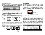
Page 19: ...ble lines is reduced to 480 because of the time required for V H retrace creating a blanking area above and below the picture Therefore the standard resolution NTSC signal displays a 480i picture 480 is the number of lines in the total picture The i suffix identifies an interlaced picture Since the picture is interlaced there is only half the number of lines presented in a single scan In this case...

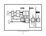
Page 20: ...IC3414 YUV SWITCH IC3603 ID 1 DECODE IC201 Y C CRT DRIVE TUNER VIDEO 1 4 STANDARD NTSC RESOLUTION VIDEO 5 VIDEO 6 480i 480p 1080i H V SYNC 480i 480i H V CRT CATHODES VERT OUTPUT IC5004 D BD OSD CONT Y Pb Pr Y Pb Pr DATA CLK IIC BUS IIC BUS DATA CLK B BD A BD C BD 12DTV02 1080i 480p 10 2 00 VIDEO Yo 7 Cr 7 Cb 7 ...

Page 21: ...oving images Each interlaced field displays a slightly different transitioning picture making movement seem smoother In the interlaced scan mode the DRC circuit still must double the number of lines to meet the TV s 480 line scan requirement The resolution is changed from 480i actually 240 lines to 960i actually 480 lines by the DRC circuit MID Circuit Fortunately the model KV32XBR400 TV s horizon...

Page 22: ...IC3414 YUV SWITCH IC3603 ID 1 DECODE IC201 Y C CRT DRIVE TUNER VIDEO 1 4 STANDARD NTSC RESOLUTION VIDEO 5 VIDEO 6 480i 480p 1080i H V SYNC 480i 480i H V CRT CATHODES VERT OUTPUT IC5004 D BD OSD CONT Y Pb Pr Y Pb Pr DATA CLK IIC BUS IIC BUS DATA CLK B BD A BD C BD 12DTV02 1080i 480p 10 2 00 VIDEO Yo 7 Cr 7 Cb 7 ...

Page 23: ... video format is a high resolution picture with a 16 9 aspect ratio at a 33 75kHz horizontal frequency The 1080i picture actually has 540 lines scan half 1080 Although 540 lines would fill this picture tube vertically the picture tube is the wrong aspect ratio The 16 9 picture is the correct width on the TV but is too tall because it is displayed on a 4 3 picture tube To compensate the vertical si...

Page 24: ...IC3414 YUV SWITCH IC3603 ID 1 DECODE IC201 Y C CRT DRIVE TUNER VIDEO 1 4 STANDARD NTSC RESOLUTION VIDEO 5 VIDEO 6 480i 480p 1080i H V SYNC 480i 480i H V CRT CATHODES VERT OUTPUT IC5004 D BD OSD CONT Y Pb Pr Y Pb Pr DATA CLK IIC BUS IIC BUS DATA CLK B BD A BD C BD 12DTV02 1080i 480p 10 2 00 VIDEO Yo 7 Cr 7 Cb 7 ...

Page 25: ...Input CN3201 pin 1 2Vp p 2 Y Output CN3201 pin 3 2Vp p 3 C Output CN3201 pin 5 1 7Vp p Time base 20usec div Component Video Conversion B Board The separate Y C main signal is matrixed into component Y Pb and Pr signals inside IC3048 This IC3048 can therefore act as a switch to choose between the component video input from Video 5 Video 6 or the main signal from the 3D Comb filter An additional RGB...

Page 26: ... DRC CD SEL SYNC SEL MID uCOM IC3090 MAIN TUNER SUB TUNER VIDEO 1 4 480i FORMAT MONITOR OUT VIDEO 5 6 480i 480p 1080i A BD B BD U BD SUB OUT Y C TO YCT SUB IC3110 CN003 CN3203 HD S VD S IC3110 SUB VIN VIN RGB HTIM VTIM HTIM VTIM SYNC TO IC3413 MAIN Y C Y C DATA CLK I2 C BUS TO MID uCOM IC3090 VID 5 6 COMPONENT VIDEO TO IC3414 SUB Y Pb Pr IC3110 HD VD C Y CN3500 CN3201 CN3201 CN3500 TO DRC MF IC330...

Page 27: ... interconnected MID uCom IC3090 can control the signal and sync routing as well as send information to the Y C CRT Drive IC201 for verti cal reduction MID uCom IC3090 Outputs Name Destination Purpose DO CO data clock MID XA IC3408 Add 60 blank lines IIC data bus Y C CRT Drive Vertical Reduction Sync Sel Sync Sw IC3413 Sync for IC201 To summarize the MID functions 60 lines are added to the picture ...

Page 28: ...ATA CLK Y Pb Cr VIDEO SYNC SEL SYNC G2 MUTE II C BUS POWER OFF MUTE FROM MAIN uCOM IC701 67 Q708 Q730 MAIN Y Pb Pr FROM IC3002 YCT SEL HD VD SYNC FROM IC3004 DRC SYN SEL IC3410 D A OSD RGB FROM MAIN uCOM IC701 H DRIVE V DRIVE P MUTE R G B IK YO 7 CRO 7 CBO 7 H V Y CB CR MID H MID V CN202 CN9001 CN3203 CN003 YO 7 CRO7 CBO 7 C BD A BD Y Pb Pr COMPONENT VIDEO FROM IC3001 AV SW1 B BD 4BDTV02 1255 PROG...

Page 29: ...to display a picture To see the full operation in the next scope shot the red drive wire has been opened at CN9001 pin 1 The CN9001 pin 1 connector is shorted to ground to simulate a defect red cathode Notice the red IK drive pulse vertical blanking area of ch 1 is still at 3Vp p power On level The normal green signal ch 2 shows the IK signal is reduced to 1 8Vp p because the IK loop is complete T...

Page 30: ...ATA CLK Y Pb Cr VIDEO SYNC SEL SYNC G2 MUTE II C BUS POWER OFF MUTE FROM MAIN uCOM IC701 67 Q708 Q730 MAIN Y Pb Pr FROM IC3002 YCT SEL HD VD SYNC FROM IC3004 DRC SYN SEL IC3410 D A OSD RGB FROM MAIN uCOM IC701 H DRIVE V DRIVE P MUTE R G B IK YO 7 CRO 7 CBO 7 H V Y CB CR MID H MID V CN202 CN9001 CN3203 CN003 YO 7 CRO7 CBO 7 C BD A BD Y Pb Pr COMPONENT VIDEO FROM IC3001 AV SW1 B BD 4BDTV02 1255 PROG...

Page 31: ...ted the main picture moves to the right There is no swap button to exchange pictures Standard Resolution Input When only standard resolution signals are selected in the picture with picture mode the left picture will pass through the DRC MF circuit for detail improvements The right picture will enter the MID XA circuit di rectly to be reduced and merged with the main DRC picture on the same screen...

Page 32: ...ll come from the tuner or video 1 4 signals along the top 480i path through the DRC MF IC3303 The right side picture in Twin View cannot select video 5 or 6 inputs they are skipped during the selection PICTURE WITH PICTURE HIGH RESOLUTION INPUT IC9001 3 VIDEO OUT A V SWITCHES COMPOSITE TO COMPONENT MATRIX A10 IC3303 DRC MF IC3408 MID XA IC201 CRT DRIVE VIDEO 5 6 Y Pb Pr 1080i 480p 480i PIX IN DRC ...

Page 33: ... occur the front panel master ON OFF button S01 on the HA board must be pressed in This latching switch behind the button supplies the AC relay RY6501 with standby 7V Pressing the switch again would unlatch the switch and the set would shut OFF Power ON can be activated from the remote control or when the front panel button is latched in The second half of front panel switch S01 not shown grounds ...

Page 34: ...NDBY 15V DCC COIL AC RELAY 135V OVP OCP STANDBY 7V IC6501 SECONDARY POWER SUPPLY SET 9V SET 5V SET 3 3V 200V 135V SOURCE SOURCE A BD STANDBY 5V STANDBY 7V STANDBY 15V SOURCE AC OUT AC Q6527 D6530 D BD D721 D722 R6006 R6526 AC RECT F6001 6A CN6013 CN6503 CN7003 CN702 CN6504 CN6005 CN6501 CN6502 6DTV02 1261 2 5 DGC COIL MAIN RELAY MAIN RELAY PRI PRE 15V STANDBY 5V POWER ON HA BD S 01 24V AUDIO 15V 3...

Page 35: ...03 and C6009 external to IC6001 pins 10 and 14 Vb complete an internal voltage boost circuit This boost circuit starts with VC1 voltage input pin 8 that is connected internally to VC2 pin 10 less 0 6Vdc This VC2 voltage is filtered by C6009 and passes through blocking diode D6003 into pin 14 Internal pulses from IC6001 pin 14 add to D6003 s DC volt age producing the boost voltage at Vb pin 14 This...

Page 36: ... ERROR DET uPC1093C 3 1 AC RECT FROM D6530 D BD R6606 0 47 OHMS R6059 R6007 R6008 R6009 R6011 C6064 VC1 VC2 VB F B OCP R6043 T6003 Q6008 Q6007 TIMER R6049 R6050 R6022 R6029 D6011 C6014 UNREG 7V SOURCE D6005 D6009 D6012 D6013 PRI PRE 15V D BD UNREG 5V SOURCE UNREG 11V SOURCE V SENSE 7DTV02 1263 340VDC 160V 3V 1 86V D6003 18 4V A BD VD VGH VS VGL ...

Page 37: ...2 10 0V M TB1 0 0us 1 28dv ch1 1 2 T Hot ground is at CN6501 pin 6 black wire Oscillator Output Operation The details of how the oscillator develops output voltage in T6003 are explained here When the oscillator in IC6001 starts up V Sense 3V no feedback VC1 voltage yet the signal is amplified using unregulated voltage input pin 18 and a 200kHz signal is output IC6001 pins 12 and 16 This is shown ...

Page 38: ... ERROR DET uPC1093C 3 1 AC RECT FROM D6530 D BD R6606 0 47 OHMS R6059 R6007 R6008 R6009 R6011 C6064 VC1 VC2 VB F B OCP R6043 T6003 Q6008 Q6007 TIMER R6049 R6050 R6022 R6029 D6011 C6014 UNREG 7V SOURCE D6005 D6009 D6012 D6013 PRI PRE 15V D BD UNREG 5V SOURCE UNREG 11V SOURCE V SENSE 7DTV02 1263 340VDC 160V 3V 1 86V D6003 18 4V A BD VD VGH VS VGL ...

Page 39: ... to run the Secondary Power Supply Item From Purpose 340Vdc B CN6501 pin 1 Bridge Rectifier D6530 Powers the Driver Output Pri Pre 15V voltage CN6501 pin 5 Primary Power Supply secondary Starts the oscillator when more than 15 6Vdc Main Relay normally HIGH at CN6504 pin 2 Main uCom IC701 Enables IC6501 when HIGH Regulation The 135V line to the Horizontal Output stage is fed back to IC6501 for regu...

Page 40: ... D6530 DC PRI PRE 15V CN6005 6 A BD GND AU 24 TO AUDIO 200V SOURCE 135V SOURCE T6501 PIT R6526 0 1 OHM R6513 R6646 Q6507 Q6528 N STANDBY 5V START MAIN RELAY FROM MAIN uCOM IC701 72 A BD Q6531 N R6504 D6502 R6501 VC2 VC1 V B OCP Q6503 R6533 N R6535 Q6506 R6556 C6532 R6590 N CH N CH D6515 D6513 V SENSE R6557 D6517 R6552 D BD 8DTV06 1262 ON ON OFF TO HV SOURCE R6598 1 R6517 VD VGH VS VGL F B D6514 D6...

Page 41: ...ding provides 200V for the RGB video output ICs While the H DY yoke provides horizontal beam deflec tion sweep a voltage divider consisting of capacitors C5058 C5060 tap off a sample of the H spike from the H Output Q5030 Collector to start the HV converter stage This AFC PLS is also used in the convergence and dynamic focus stages The waveforms of the horizontal drive stage show typical signal sh...

Page 42: ...PUT C BD T5002 HDT CN203 CN5505 R5013 R5096 D5015 R5095 D5014 N CH Q5028 DRIVER Q5030 H OUT R5142 4 T5001 HOT D5018 50V H DY R5094 D5012 G2 TO C BD R5164 D5025 UNREG 7V A BD D5024 D5023 N C5058 C5059 C5060 CRT HEATER H PROT IC701 44 Y C A BC 135V D BD A BD HOT AFC PLS TO 14DTV02 1266 135V 102V 47 7 E W DRIVE CN201 CN5503 33 61 55 X201 MAIN 9V 7 37 AFC PLS Q5030 C HD IC8001 8 HV CONV IC5511 19 DQP ...

Page 43: ... this scope s time base Horizontal Pincushion Correction Channel Name Location Voltage 1 E W Drive Cn5505 pin 7 0 7Vp p 2 PWM Output T5001 pin 1 150Vp p 102Vdc Time base 5mesc div ch2 ch1 CH1 500mV CH2 50 0 V MTB5 00ms ch1 1 2 T Filament Voltage There are two sources of filament voltage When the set is turned ON unregulated 7V from the primary power supply A board is reduced by D5025 and D5024 to ...

Page 44: ...PUT C BD T5002 HDT CN203 CN5505 R5013 R5096 D5015 R5095 D5014 N CH Q5028 DRIVER Q5030 H OUT R5142 4 T5001 HOT D5018 50V H DY R5094 D5012 G2 TO C BD R5164 D5025 UNREG 7V A BD D5024 D5023 N C5058 C5059 C5060 CRT HEATER H PROT IC701 44 Y C A BC 135V D BD A BD HOT AFC PLS TO 14DTV02 1266 135V 102V 47 7 E W DRIVE CN201 CN5503 33 61 55 X201 MAIN 9V 7 37 AFC PLS Q5030 C HD IC8001 8 HV CONV IC5511 19 DQP ...

Page 45: ...V9002 varies the conduction of Q9012 and Q9014 and conse quently the shunt resistance A lower shunt resistance produces a lower G2 voltage The G2 voltage range of the screen control is listed in the chart G2 RV9002 Voltage Range RV9002 Position G2 Voltage CCW 292 4Vdc Normal 484Vdc 2 3 CW 590Vdc is maximum before shutdown Operating Voltages Normal Operating Voltages Transistor Collector Base Emitt...

Page 46: ...62 100k R9056 100k 484VDC CRT G2 GRID D9001 D9003 R9004 R9005 Q9002 MUTE C9038 4 7 R9010 10k R9009 10k FROM MAIN uCOM IC701 67 A BD R9078 C9036 10 10 4V 5 4V R9067 R9076 Q9012 G2 REF D9015 PROT Q9008 G2 REF Q9014 G2 REF R9063 100k 1 2W RV9002 100k G2 R9063 D9017 PROT D9016 PROT C9047 0 01 CHIP R9081 C9037 2 2 R9079 POWER OFF MUTE N N N N C BD 18DTV02 1267 ...

Page 47: ...e without affecting the sound The second circuit shuts down the entire TV set if the 200V current de mand is excessive Excessive HV Protection The HV oscillator in IC8002 is stopped if the HV sampled from the flyback is excessive The oscillator stops when via Q8003 or Q8004 grounds IC8002 pin 1 Sample high voltage from the flyback transformer normally takes two paths to keep Q8003 and Q8004 turned...

Page 48: ...PICTURE TUBE FOCUS VOLTAGE PICTURE TUBE DF DRIVE DQP CONTROL IC5511 11 200V FROM SECONDARY POWER SUPPLY AFC PLS Q5030 C H OUT Q8001 Q8002 C8004 100 ON OFF Q8004 OFF OFF Q8003 R8053 R8055 V SENSE RV8002 HV F B D8004 5 1V D8014 C8005 47 D8020 Q8010 D8025 33V R8078 9DTV02 1264 RV8001 COARSE RV8003 FINE R8042 START HV CONV D8003 SHUTDOWN LATCH Q6530 Q6532 D BD Q8009 OCP 18 VD 8 VC1 15V SEC P S R8056 ...

Page 49: ...r Check If no HV is output look for 200V input at IC8002 pin 18 and more than 15 6V at IC8002 pin 8 Look for HV Conv start voltage at IC8002 pin 1 normally 1 6Vdc but must be more than 1 3Vdc to start Converter IC8002 Voltages Pin 1 2 3 4 5 6 7 8 9 Volts 1 63 1 75 2 25 2 47 0 0 4 56 14 7 0 Pin 10 11 12 13 14 15 16 17 18 Volts 10 3 0 4 14 0 108 98 6 103 0 200 Additional Important Voltages related t...

Page 50: ...PICTURE TUBE FOCUS VOLTAGE PICTURE TUBE DF DRIVE DQP CONTROL IC5511 11 200V FROM SECONDARY POWER SUPPLY AFC PLS Q5030 C H OUT Q8001 Q8002 C8004 100 ON OFF Q8004 OFF OFF Q8003 R8053 R8055 V SENSE RV8002 HV F B D8004 5 1V D8014 C8005 47 D8020 Q8010 D8025 33V R8078 9DTV02 1264 RV8001 COARSE RV8003 FINE R8042 START HV CONV D8003 SHUTDOWN LATCH Q6530 Q6532 D BD Q8009 OCP 18 VD 8 VC1 15V SEC P S R8056 ...

Page 51: ... network 1 receive this data to set their operating parameters the TV can function The Y C CRT Drive IC201 on the A board and MID uCom IC3090 on the B board can provide return reply data to IC701 This data either up dates the on screen display menu OSD is in IC701 or initiates a safety shutdown of the TV The data at both network 0 and network 1 is always present as long as the TV is ON The first s...

Page 52: ...01 COMP I F IC3090 MID uCOM IC3201 A V SW IC3202 AUDIO SW IC3601 SUB CCD V CHIP IC3408 Y CT MAIN IC3089 NVM IC3408 MID XA IC3110 Y CT SUB IC3602 MAIN CCD V CHIP IC5513 DY CONV IC4103 AUDIO D A STBY 5V STBY 5V STBY 5V DAT 1 CLK 1 WP CLK 0 DAT 0 Q717 RESET CLK DATA R829 R827 R834 IIC BUS STBY 5V WP DATA BC BD CN706 CN5501 CN703 CN6506 CN702 CN6504 CN7001 CN4104 CLK CN3201 CN3500 S BD A BD D BD B BD ...

Page 53: ...25 0 0V M T B 5 0 0 m s 1 3 2 d vHxx 1 2 T Network 1 Communications TV Channel 7 displayed Scope Channel Name Location Voltage 1 Clock CN706 pin 7 5Vp p 2 Data CN706 pin 8 5Vp p Time base 5msec div Communications Network 2 Communications network 2 is only used between three ICs on the B board MID uCom IC3090 communicates with MID IC3408 to retrieve processed data such as the input horizontal frequ...

Page 54: ...01 COMP I F IC3090 MID uCOM IC3201 A V SW IC3202 AUDIO SW IC3601 SUB CCD V CHIP IC3408 Y CT MAIN IC3089 NVM IC3408 MID XA IC3110 Y CT SUB IC3602 MAIN CCD V CHIP IC5513 DY CONV IC4103 AUDIO D A STBY 5V STBY 5V STBY 5V DAT 1 CLK 1 WP CLK 0 DAT 0 Q717 RESET CLK DATA R829 R827 R834 IIC BUS STBY 5V WP DATA BC BD CN706 CN5501 CN703 CN6506 CN702 CN6504 CN7001 CN4104 CLK CN3201 CN3500 S BD A BD D BD B BD ...

Page 55: ...be glass screens were made into a similar arc to maintain focus at the left and right sides of the screen This means the focus point must be moved up at the left and right sides to meet the flat picture tube screen Dynamic Focus Concept The job of the dynamic focus circuit is to change the focus points to meet the flat picture tube screen This is done by either increasing the static focus voltage ...

Page 56: ...EEN DF FOCUS CORRECTION IC5502 NJM2901M VTIM CN5503 2 Y C CRT DRIVE IC201 54 T8001 FLYBACK HV CONV CRT HV CRT FOCUS VOLTAGE R8082 Q5501 C5509 R8102 C8051 10 T8002 DFT 135V P R8101 Q8016 SW C8060 4 7 160V Q8015 SW L8005 D8017 DATA CLK IIC BUS SWO DAC1 AFC PLS H OUT Q5030 C 22k C8058 Q8018 DF OUTPUT N D BD 15DTV 1268 6 4 3 91VDC 1 SM CATEGORY 2026AS DF ON 0 ON 1 OFF DF CHANGES FOCUS START ...

Page 57: ...her near the FBT The final DF Output transistor Q8018 applies the signal to T8002 pin 3 In the following waveforms you can see the low going drive signal from IC5511 pin 11 ch 2 become inverted and delayed ch 3 The final drive signal ch 4 goes low to reduce the focus voltage at the right side of the picture Modulated power supply The modulated power supply signal is also made in IC5511 from horizo...

Page 58: ...EEN DF FOCUS CORRECTION IC5502 NJM2901M VTIM CN5503 2 Y C CRT DRIVE IC201 54 T8001 FLYBACK HV CONV CRT HV CRT FOCUS VOLTAGE R8082 Q5501 C5509 R8102 C8051 10 T8002 DFT 135V P R8101 Q8016 SW C8060 4 7 160V Q8015 SW L8005 D8017 DATA CLK IIC BUS SWO DAC1 AFC PLS H OUT Q5030 C 22k C8058 Q8018 DF OUTPUT N D BD 15DTV 1268 6 4 3 91VDC 1 SM CATEGORY 2026AS DF ON 0 ON 1 OFF DF CHANGES FOCUS START ...

Page 59: ...n ning lines in the picture Dynamic focus can be turned ON OFF and phase adjusted start loca tion in the service mode Data group 7 with the heading 2026 con tains two items related to dynamic focus Service Mode Category 2026 Item Name Purpose DFON Data 0 dynamic focus ON Data 1 dynamic focus OFF DF Positions IC5511 pin 14 switching pulses to change the start of the dynamic focus points on the scre...

Page 60: ...EEN DF FOCUS CORRECTION IC5502 NJM2901M VTIM CN5503 2 Y C CRT DRIVE IC201 54 T8001 FLYBACK HV CONV CRT HV CRT FOCUS VOLTAGE R8082 Q5501 C5509 R8102 C8051 10 T8002 DFT 135V P R8101 Q8016 SW C8060 4 7 160V Q8015 SW L8005 D8017 DATA CLK IIC BUS SWO DAC1 AFC PLS H OUT Q5030 C 22k C8058 Q8018 DF OUTPUT N D BD 15DTV 1268 6 4 3 91VDC 1 SM CATEGORY 2026AS DF ON 0 ON 1 OFF DF CHANGES FOCUS START ...

Page 61: ...ed to the four QP coils At power ON Q5008 and Q5505 use C5027 to momentary disable the DQP amplification in IC5504 This is so the beam will be unaffected by incorrect voltages at start up Q5502 Q5507 and IC5502 monitor the horizontal width AFC PLS from Q5030 and corrects for focus if the width changes momentarily This is accomplished by changing the DC input voltage of IC5504 pin 2 propor tional t...

Page 62: ...RA 2 AFC PLS Q5030 C VTIM CN5503 2 IC201 54 R5696 C5614 IIC BUS FROM IC701 28 31 C5531 0 1 D5514 D5515 R5564 C5533 R5563 R5554 18k L5504 C5548 0 47 R5588 L5505 CN5509 QP QP MAIN 12V R5056 C5027 R5577 180k PARA 1 HORIZ AFC PLS Q5030 C 67DTV02 1282 6 4 ADJUSTMENT SERVICE MODE CATEGORY 2026AS DQP FOCUS CORRECTION ITEM 1 DQP PWM LEVEL ITEM 3 DQPD DC LEVEL ITEM 4 QPDV VERT MOD ITEM 5 DVS TILT ITEM 7 DQ...

Page 63: ...300Vp p Time base 10usec div PM3394 FLUKE PHILIPS ch2 ch1 CH1 50 0 V CH2 100 V MTB10 0us 1 18dv L xx 1 2 T Adjustment The waveforms from IC5511 can be changed from the service mode to affect the starting point of focus correction on the screen the amount of focus and convergence These items are found in the service mode category 2026AS ...

Page 64: ...RA 2 AFC PLS Q5030 C VTIM CN5503 2 IC201 54 R5696 C5614 IIC BUS FROM IC701 28 31 C5531 0 1 D5514 D5515 R5564 C5533 R5563 R5554 18k L5504 C5548 0 47 R5588 L5505 CN5509 QP QP MAIN 12V R5056 C5027 R5577 180k PARA 1 HORIZ AFC PLS Q5030 C 67DTV02 1282 6 4 ADJUSTMENT SERVICE MODE CATEGORY 2026AS DQP FOCUS CORRECTION ITEM 1 DQP PWM LEVEL ITEM 3 DQPD DC LEVEL ITEM 4 QPDV VERT MOD ITEM 5 DVS TILT ITEM 7 DQ...

Page 65: ...utput at IC5513 pin 8 corrects for left and right mis conver gence The V Stat output at IC5513 pin 9 corrects for top and bottom mis convergence The two signals are combined externally and amplified by IC5515 into a 10Vp p waveform at the convergence yoke CN5510 pin 3 IC5513 s input and output signals are listed in the chart IC5513 s Input Output Signals Name IC5513 pin Voltage Purpose VTIM 3 1 8V...

Page 66: ...9 1 2 3 8 4 3 1 10 R5699 V STAT R5693 H STAT 5V REF CY PART OF MAIN YOKE CN5510 15V 15V MAIN 12V SOURCE VTIM IC201 54 AFC PLS Q5030 C R5648 R5712 R5711 IC5515 STK390 910 DATA CLOCK IIC BUS 15V D BD 16DTV02 1272 IC5003 12V REG SERVICE MODE CATEGORY D CONV 9 ADJUSTMENT ITEMS ...

Page 67: ...izontal trapezoid correction sawtooth signal are created by IC201 The signal and DC voltage leave IC201 pin 51 and are amplified by IC5510 before being sent to the N S coil The voltages in normal operation and when the user has set the tilt to both extremes 7 are shown in the chart Tilt correction Voltages Location Name 0 rotation 7 rotation 7 rotation CN201 pin 5 Output of IC201 4Vdc 5Vdc 3Vdc CN...

Page 68: ...IC BUS DATA CLK1 CLK O V SAW 1 DATA O LA6500 R5678 R5679 C5601 12V R5669 R5670 MAIN 12V R5613 270 R5705 1 0 25V 4V CN201 CN5503 CN5509 CN9102 D BD N S COIL A BD 0V 66DTV02 1281 11 12 R5688 N S COIL YOKE PICTURE TUBE REAR 38 2 OHMS ADJUSTMENTS USER SERVICE MODE SET UP MENU TILT CORRECTION CATEGORY 2150D 1 ITEM 6 NSCO 0 15 ITEM 7 HTPZ HORIZ TRAPEZOID ...

Page 69: ... vertical components This signal is amplified by IC5514 and applied to the pincushion coil The correction signals before and after amplifier IC5514 is shown in this scope shot Vertical Pincushion Correction Signal Channel Name Location Voltage 1 VSAWO CN201 pin 6 0 3Vp p 2 Pincushion Output CN5509 pin 2 0 5Vp p main waveform 3 5Vp p including spike Time base 5msec div The Vertical Pincushion coil ...

Page 70: ...2 4 5 3 W BD IIC BUS DATA CLK1 CLK O V SAW O DATA O IC5514 V PIN OUT LA6500 R5700 R5615 C5616 12V R5697 R5698 MAIN 9V R5710 270 R5704 1 0 25V 4V CN201 CN5503 CN5509 CN9102 CRT V PIN V PIN A BD D BD 0V 20DTV02 1271 SLIGHT BOW INWARDS NO CORRECTION 1 2 SM CATEGORY 2150D 1 5 ITEMS ADJ IN ALL 3 MODES 1 FULL NORMAL 2 V COMP1 480P 16 9 3 V COMP2 1080I VERT ENHANCED ...

Page 71: ...oke To make sure the vertical stage is operational a sample of the vertical signal is returned to IC201 pin 35 If IC201 detects a loss of vertical pulses it blanks the picture If the loss remains for two seconds IC201 sends data to Main uCom IC701 to shut down the set and store the vertical failure code Vertical pulses from IC5004 pin 3 are sent to the MID uCom IC3090 pin 35 to identify the end of...

Page 72: ...N R5018 CN5002 D5001 5 1V V SYNC FOR OSD MAIN uCOM IC701 97 VFB TO MID uCOM IC3090 35 B BD FOR PROG INTER TIMING CN201 CN5503 CN3205 CN003 CN706 CN5501 V SYNC PROGRESSIVE V SYNC FROM IC3408 VTIM INTERLACE FROM IC3048 15 YCT MAIN SEL V OUT SUB PIX FROM IC3001 23 COMP J F SYNC SEL IC3090 10 MID uCOM TH CONT X SW IC701 52 A BD Y C CRT DRIVE V DRV PROT A BD B BD 13DTV02 1269 55 CN203 CN5505 61 MAIN 9V...

Page 73: ...The vertical ramp s amplitude is also reduced This can be seen when comparing the normal and compressed vertical waveform Notice there is an irregularity at the beginning of the vertical ramp in the compressed vertical mode PM3394 FLUKE PHILIPS ch2 ch1 ch2 pkpk 1 78 V ch2 freq 122Hz CH1 2 00V CH2 500mV MTB2 00ms 0 90dv ch1 1 2 T Normal vertical ramp Vertical Drive Signal Normal Channel Name Locati...

Page 74: ...N R5018 CN5002 D5001 5 1V V SYNC FOR OSD MAIN uCOM IC701 97 VFB TO MID uCOM IC3090 35 B BD FOR PROG INTER TIMING CN201 CN5503 CN3205 CN003 CN706 CN5501 V SYNC PROGRESSIVE V SYNC FROM IC3408 VTIM INTERLACE FROM IC3048 15 YCT MAIN SEL V OUT SUB PIX FROM IC3001 23 COMP J F SYNC SEL IC3090 10 MID uCOM TH CONT X SW IC701 52 A BD Y C CRT DRIVE V DRV PROT A BD B BD 13DTV02 1269 55 CN203 CN5505 61 MAIN 9V...

Page 75: ...ain signal Sub signal Video 5 Video 6 Selection of Main Vs Sub sound is used in the Twin mode The outputs go to the rear monitor output jack and the S board for TruSurround Sound processing S Board The L R channel audio is applied to both TruSurround IC4101 and Switch IC4102 The TruSurround IC4101 outputs the L R audio if the TruSurround mode is not selected When TruSurround is selected the second...

Page 76: ...OCESSOR BH3868 IC7002 POWER AMP TA8216 IC7006 LOW PASS NJM4558 IC7005 POWER AMP TA8216 IC7007 BUFFER NJM4558 1 7 3 5 HIGH PASS AUDIO 5 AUDIO 6 AUDIO 3 AUDIO 2 AUDIO 1 SUB MAIN INPUTS THICKER LINES DENOTE L R SIGNAL PAIR MONITOR OUT LINE OUT DATA CLK IIC BUS IIC BUS CN7008 CN7001 CN4101 CN3205 CN003 MAIN SUB MON L R H L H R W L W R SPEAKERS B BD A BD S BD 17DTV02 1270 5 7 IC3201 ANALOG SW A V CXA20...

Page 77: ...06 pin 8 0V 3 X Shutdown A Unreg 7V OVP D6017 C 0V 3 X Shutdown D 135V OVP CN6506 pin 7 0 1V 4 X Shutdown D V Out Loss CN5505 pin 7 0 78V 5 X Blanking C A G2 adj IK balance CN202 pin 8 3 pulses in vertical interval 6X Shutdown A Set 5V OCP IC6007 Output 5 0Vdc 7X Shutdown D H Out OCP CN5505 pin 8 0V TV latched OFF Press power button twice to turn TV back on OSD Diagnostics In addition to the blink...

Page 78: ...GB LOW B OCP UNREG 7V DATA CLK SET 5V RGB TO CRT IK SIGNAL WHITE BAL FAILURE V OUT LOSS H OUT OCP CN203 CN5505 CN202 CN9001 CN6506 CN703 AC RELAY ON OFF CN6504 CN702 STANDBY LED 7 8 IC201 Y C CRT DRIVE 8 7 8 C BD D BD D BD D6018 D6017 10DTV02 1260 1 NUMBER OF TIMES THE STANDBY LIGHT BLINKS AFTER SHUTDOWN X 3 X 0 X 2 X 0 X 3 X 6 X 5 X 4 X 7 X ...

Page 79: ...e sensing circuit on this A board Verify this problem by monitoring CN6506 pin 8 as you power ON If the voltage does not rise above 0v at power ON the problem is not on the 135V line If the voltage reaches 1 2V disconnect the V board and try again If the CN6506 pin 8 voltage still rises to 1 2V test the H Output and PWM transistors or replace the entire D board Shutdown Standby light blinks three ...

Page 80: ...15 1k IC701 MAIN uCOM OCP OVP D BD A BD R6593 R6598 R6591 STBY 5V R6612 Q6524 P P 135V SEC P S 135V SOURCE 15V Q6527 AC FROM F BD 200V TO HV CONV 200V SEC P S R8043 1 OHM D8003 D6537 OVP OCP Q6522 D6501 AC TO 200V 135V POWER SUPPLY AC RELAY CN6506 CN703 CN6504 CN702 D6018 UNREG 7V SET 5V SOURCE STANDBY LED TO FROM YC CRT DRIVE IC201 26 27 DAT O CLK O UNREG 7V PRI P S 11aDTV02 1258 48 ...

Page 81: ...blink two times and the second will cause the light to blink seven times Both sensing and output circuits are on the D board but the indicating circuit is on the A board Circuit The second OCP circuit monitors the current through the PWM Output Q5001 3 that supplies B voltage to the H Output transistor Q5030 When there is excessive current drawn by the Horizontal Output stage Q5018 turns OFF permi...

Page 82: ... YOKE HDT T5001 1 H OUT Q5030 135V N C219 0 068 25V R9006 12V CN202 CN9001 R9065 Q9001 P R9012 R9008 D9002 12V IK FROM IC9001 5 IC9002 5 IC9003 5 R9068 R5013 C5006 10 IC5007 COMPARATOR MAIN 9V R5108 R5108 Q214 PROT MUTE MAIN uCOM IC701 54 N Q5018 H PROT R250 R249 V PROT MAIN 9V R5599 10k R5125 R5104 MAIN 12V R5046 1 8 OHMS R5052 1 5 OHMS OUT CN5002 5 CN203 CN5505 A BD C BD D BD IK 11bDTV02 1259 ...

Page 83: ...APPENDIX ...
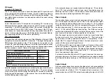
Page 84: ...d by the MID circuit when measuring the hori zontal frequency of the signal input The default format is 480i when there is no video signal input Input signal Horizontal Frequency Standard NTSC 480i 15 734 Hz High Resolution 480p 31 5kHz High Resolution 1080i 33 75kHz Bottom Flag numbers These numbers are added in manufacturing to identify where the boards come from and when they were made The info...

Page 85: ...0 1450Hz Transport Demultiplexer Video Decoder MPEG 2 Audio Decoder Dolby AC 3 NTSC Encoder S Video Composite Video Ch 3 4 RF Output IEEE 1394 i LINK Analog Audio Optical Out Digital RJ11 phone jack Low speed data 9 pin D sub Interface Modulator audio video video audio access card 41DTV02 DSS Dish ...

Page 86: ...ignal feed Antenna VSB Demodulator Transport Packet Demultiplexer Micro VIDEO Decompression MPEG 2 AUDIO Decompression Dolby AC 3 Analog L R Digital Optical Port Composite Video Componet Video Y Pb Pr S Video or Format Decoder Down Conversion ...

Page 87: ...terminators Peer to peer communications are possible Any device should com municate with any other device without the need for a hub or a PC to be connected The system uses scalable architecture that will allow older slower devices to communicate with newer faster devices at the slower rate Different combinations of faster and slower devices can be used on the same bus Hardware There is hardware c...

Page 88: ...a predetermined rate and not checked for accuracy Dynamic Node Addressing Each device called a node is assigned a specific address This occurs when a bus reset occurs or a new device is added to the system Three steps occur when these events occur IDs Cleared All previous ID information is erased Tree ID The device which is the bus master assigns each node a specific address This is called the Tre...

Page 89: ...ef list of products that use IEEE 1394 are DV Camcorders D8mm Camcorders High Resolution Digital Cameras HDTV HDTV Set Top Converter Boxes DSS Digital Satellite System Boxes Hard Disks DVD ROM Drives Printers Scanners Future Developments IEEE1394 seems poised to take its place as the home networking stan dard of the future Its high speed and ease of use are part of the keys that may one day make i...

Page 90: ...BUSCONN CN3204 B B B B U U U U CN203 CN201 CN6005 CN607 CN605 DGC S S S S W W W W C C C C CN603 AC CORD TO SPEAKERS TO SPEAKERS CN9001 CN9002 ANT ANT ANT ANT SW SW SW SW CN202 CN204 FOCUS LEAD HV LEAD CN707 12mm Purse Lock 38mm height CN7004 MAIN MAIN MAIN MAIN SUB SUB SUB SUB TO DY CN9102 CN9103 N S CN9101 DX 1A CHASSIS ASSEMBLY CL701 HV REG BLOCK Optional BC BC BC BC 9 Put one loop in HV Lead an...

Page 91: ...HV shutdown RV8001 coarse and RV8003 fine according to safety related adj in the service manual A Remove 4 screws from the rear panel and fold it down Pry the locks from connectors CN3202 3 while wiggling the B board away form the A board Remove 6 screws securing the A board Lift the right side of the A board out Standby Power Supply Degaussing circuit Secondary Power Supply 9V 5V 3 3V H V Oscilla...

Page 92: ...control according to the service manual Reduce vertical size to see IK line at the top Blank pix in the service mode by changing CXA2150P 2 ALBLK data from 0 to 1 Adjust screen control so the IK line is just invisible in a dark room W Remove the C board Mark the pix tube neck to reinstall the new W board assembly Loosen the clamp and remove the assembly Velocity Modulation circuit to improve detai...

Page 93: ...x Front of TV D Board A Board HA board HB board U board B board BC board Pry out CN3202 CN3203 Pry out BC board U board ...

Page 94: ... sure it is 135 3 1 Vdc 2 Confirm Vd at pin 2 CN6506 or at TP Vd for 4 9 V Vd 5 1 Vdc 3 Apply 5 5 0 5 VDC at pin 2 of CN6544 then confirm set holds down Correct Confirm B Vd and check hold down on D board with black video with the following steps 1 Confirm B across C6544 to make sure it is 135 3 1 Vdc 2 Confirm Vd at pin 2 CN5506 or at TP Vd for 4 30 V Vd 4 65 V 3 Apply 5 5 0 3 VDC at pin 2 of CN5...

Page 95: ...onics Inc 1 Sony Drive Park Ridge New Jersey 07656 DTV021000 Printed in U S A S and i LINK aretrademarksofSonyElectronics Dolby Digital is a trademark of Dolby Fire Wire is a trademark of Apple Computer Inc TiVo is a registered trademark of TiVo Inc ...

Reviews: