background image

– 14 –

KV-HA21M80/HA21N70/HA21N80

RM-969

RM-968

The following adjustments should be made when a complete

realignment is required or a new picture tube is installed.

These adjustments should be performed with rated power

supply voltage unless otherwise noted.

Controls and switches should be set as follows unless otherwise

noted:

PICTURE control ...........................................................  normal

BRIGHTNESS control ...................................................  normal

Perform the adjustments in the following order :

1. Beam Landing

2. Convergence

3. Focus

4. White Balance

Note :

  Test Equipment Required.

1. Pattern Generator

2. Degausser

3. Oscilloscope

SECTION 3

SET-UP ADJUSTMENTS

................................................................................................................................................................................................................................

normal

Preparation :

In order to reduce the influence of geomagnetism on the
set's picture tube, face it east or west.
Switch on the set's power and degauss with the degausser.

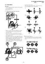
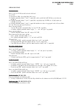
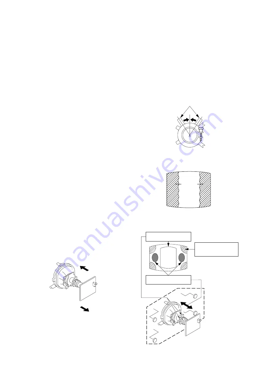
3-1. BEAM LANDING

1. Input a white signal with the pattern generator.

Contrast
Brightness

2. Set the pattern generator raster signal to a green raster.
3. Move the deflection yoke to the rear and adjust with the

purity control so that the green is at the center and the blue
and the red take up equally sized areas on each side.
(See Figures 3-1 through 3-4.)

4. Move the deflection yoke forward and adjust so that the

entire screen is green. (See Figure 3-1.)

5. Switch the raster signal to blue, then to red and verify the

condition.

6. When the position of the deflection yoke has been decided,

fasten the deflection yoke with the screws and DY spacers.

7. If the beam does not land correctly in all the corners, use a

magnet to adjust it.
(See Figure 3-4.)

}

Fig. 3-1

Fig. 3-4

Fig. 3-3

Fig. 3-2

Purity control

Red

Blue

Green

Deflection yoke positioning

corrects these areas.

Purity control corrects

this area.

Disk magnets or rotatable
disk magnets correct
these areas (a-d).

b  

c

a

d

b

a

c

d

Summary of Contents for KV-HA21N70

Page 1: ......

Page 2: ...REVISION HISTORY BG2T MODEL KV HA21M80 KV HA21N70 KV HA21N80 PART NO 9 872 280 02 CHASSIS NO SUFFIX DATE SUPP CORR DESCRIPTION 1 2 01 02 1st Issue Rear Cover Assy Suffix Change P 61 2002 1 2002 6 Supp 1 ...

Page 3: ...80 RM 969 India SCC U74C A KV HA21N70 RM 968 Philippines SCC U76D A KV HA21N80 RM 968 Philippines SCC U76C A TV 1 2 3 4 6 7 8 9 0 5 JUMP SOUND MODE SPACE SOUND PROGR 2 TV 1 2 3 4 6 7 8 9 0 5 ENT WAKE UP SLEEP JUMP CABLE DISPLAY MUTING POWER MTS VOL CH VIDEO SOUND MODE SPACE SOUND AUTO PROGRAM ADD ERASE TV RM 968 RM 969 ...

Page 4: ...NTSC4 43 AN IN only KV HA21N70 HA21N80 Channel coverage B G VHF E2 to E12 UHF E21 to E69 CATV S01 to S03 S1 to S41 KV HA21M80 I UHF B21 to B68 CATV S01 to S03 S1 to S41 KV HA21M80 D K VHF C1 to C12 R1 to R12 UHF C13 to C57 R21 to R60 CATV S01 to S03 S1 to S41 Z1 to Z39 KV HA21M80 M VHF A2 to A13 UHF A14 to A79 CATV A 8 to A 2 A to W 4 W 6 to W 84 KV HA21M80 M VHF 2 to 13 UHF 14 to 69 CATV 1 to 125...

Page 5: ...3 4 G2 SCREEN and White Balance Adjustments 17 4 CIRCUIT ADJUSTMENTS 4 1 Adjustment With Commander 18 4 2 Adjustment Method 18 4 3 Picture Quality Adjustment 28 4 4 Deflection Adjustment 28 4 5 A Board Adjustment After IC003 MEMORY Replacement 28 4 6 Picture Distortion Adjustment 29 Section Title Page Section Title Page 5 DIAGRAMS 5 1 Block Diagram 30 5 2 Circuit Boards Location 32 5 3 Schematic D...

Page 6: ...oes not turn on B overcurrent OCP Horizontal deflection overdrive White balance failure no PICTURE Vertical deflection stopped Micro reset Detected Symptoms Power does not come on No power is supplied to the TV AC power supply is faulty Power does not come on Load on power line is shorted Has entered standby state after horizontal raster Power line is shorted or power supply is stopped Vertical de...

Page 7: ...ccurances of failure for confirmation on the screen To Bring Up Screen Test In standby mode press buttons on the remote commander sequentially in rapid succession as shown below Screen display channel 5 Sound volume Power ON Note that this differs from entering the service mode mode volume Self Diagnosis screen display STANDBY SLEEP lamp Lamp ON 0 3 sec Lamp OFF 3 sec Lamp OFF 0 3 sec 2 times 4 ti...

Page 8: ...entire self diagnostic screen turn off the power switch on the remote commander or the main unit 6 SELF DIAGNOSTIC CIRCUIT B overcurrent ªOCPº Occurs when an overcurrent on the B 135 line is detected by Q500 If Q500 go to ON and the voltage to pin 50 of IC301 more than 3 5V when V SYNC is more than seven verticals in a period the unit will automatically turn off Vertical deflection stopped Occurs ...

Page 9: ...vent fire or shock hazard do not expose the TV to rain or moisture Do not operate the TV if any liquid or solid object falls into it Have it checked immediately by qualified personnel only Do not open the cabinet and the rear cover of the TV as high voltages and other hazards are present inside the TV Refer servicing and disposal of the TV to qualified personnel Your TV is recommended for home use...

Page 10: ...ers or other electrical equipment away from the TV Press main power to turn off the TV for about 15 minutes then turn it on again to demagnetize the TV Count the number of times the 1 standby indicator flashes Press main power to turn off your TV Contact your nearest Sony service center Changes in room temperature sometimes make the TV cabinet expand or contract making a noise This does not indica...

Page 11: ...r 90 minutes POWER WAKE UP SLEEP KV HA21N80 HA21N70 I Setting the timers You can turn on and off your TV by using the and buttons respectively Setting the Wake Up timer 1 Press until the desired period of time appears on the screen The Wake Up timer starts immediately after you have set it 2 Select the program number or video input you want to wake up to 3 Press 1 or set the Sleep timer if you wan...

Page 12: ... screen 2 Press or to select the appropriate color system until the color is optimal AUTO PAL SECAM NTSC3 58 NTSC4 43 To skip program numbers 1 Press PROGR or the number buttons until the unused or unwanted program number appears on the screen 2 Press SELECT until MANUAL PROGRAM appears on the screen 3 Press or once to enter the MANUAL PROGRAM mode 4 Press PIC MODE to skip the unused or unwanted p...

Page 13: ...high contrast pictures STANDARD view normal contrast pictures SOFT view mild pictures Selecting the sound mode Press SOUND MODE to select the desired sound mode Select To 9 DYNAMIC listen to dynamic and clear sound that emphasizes the low and high sound 9 DRAMA listen to sound that emphasizes vocals and background music 9 SOFT listen to soft sound Adjusting the picture and sound settings 1 Press S...

Page 14: ...L 2 2 SPEAKER REMOVAL 2 3 CHASSIS ASSY REMOVAL 2 4 SERVICE POSITION Caution Do not take out CRT support block while TV set in standing position Note Undress necessary wires that creates tension while placing the chassis into Service Position 1 Eight screws BVTP 4 16 1 Two screw BVTP 4 16 2 Rear cover 1 Two screws washer head 3 Speaker 2 Bracket Speaker P 4 16 A board Terminal board bracket One scr...

Page 15: ...caps with sharp shaped objects 2 Do not press the rubber too hard so as not to damage the inside of anode cap A metal fitting called the shatter hook terminal is built into the rubber 3 Do not turn the foot of rubber over too hard The shatter hook terminal will stick out or damage the rubber a a b b c Anode Button 2 7 PICTURE TUBE REMOVAL Note Please make sure the TV set is not in standing positio...

Page 16: ... BEAM LANDING 1 Input a white signal with the pattern generator Contrast Brightness 2 Set the pattern generator raster signal to a green raster 3 Move the deflection yoke to the rear and adjust with the purity control so that the green is at the center and the blue and the red take up equally sized areas on each side See Figures 3 1 through 3 4 4 Move the deflection yoke forward and adjust so that...

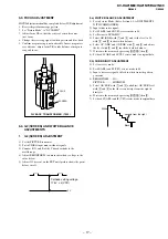
Page 17: ...lue dots together at the center of the screen adjust the horizontal convergence with the H STAT variable resistor and the V STAT magnet in the manner given below In this case the H STAT variable resistor and the V STAT magnet influence each other so be sure to perform adjust ments while tracking 1 3 R G B G R B Center dot C3 board RV 702 V STAT Magnet H STAT VR BMC Hexapole V STAT Purity V STAT BM...

Page 18: ...or Right YCH Rotate YCH VOL on DY TLV Rotate TLV VOL ON DY XCV Rotate XCV Adj core on DY ON DY 2 Dynamic Convergence Adjustment Preparation Before starting this adjustment adjust the horizontal static convergence and the vertical static convergence RB TLV YCH B R YCH TLV a d c b a to d Permalloy assembly Fix a Permalloy assy corresponding to the misconverged areas ...

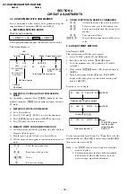
Page 19: ...ing voltage 175 V 2 VDC 2 a WHITE BALANCE ADJUSTMENT 1 Set to Service Mode Refer Section 4 1 ADJUSTMENTS WITH COMMANDER 2 Input white raster signal 3 Set 49 ABL and IF VP2 service mode to 00 4 Set Picture to DYNAMIC 5 Select OB RDR with 1 and 4 and set the level to 25 with 3 and 6 for best white balance 6 Select OC GDR and OD BDR with 1 and 4 and adjust the level with 3 and 6 for the best white ba...

Page 20: ...tandard is 1F for PAL reception 4 Write with the MUTING button The display changes to WRITE 5 Execute the writing with the button The WRITE display will be changed to red color while excuting and back to SERVICE Example on screen display 1 4 Select the adjustment item 3 6 Raise lower the data value MUTING Writes Executes the writing e OTHER FUNCTION VIA REMOTE COMMANDER 7 All the data becomes the ...

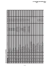
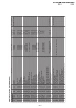
Page 21: ... O F 0 0 3 0 t n a t s n o C e m i T 1 0 t x e t e l e T o e d i V V T 2 3 0 0 6 1 T G A 0 0 F 3 r e v O e k a T C G A t x e t e l e T o e d i V V T 0 5 3 1 7 1 W S V 0 0 1 0 h c t i w S e t u M o e d i V t x e t e l e T o e d i V V T 6 3 1 8 1 R O F 3 0 3 0 y c n e u q e r F d l e i F d e c r o F 6 7 1 0 9 1 L D 0 0 1 0 e c a l r e t n i e D 5 1 0 A 1 C O P 0 0 1 0 e d o M o r h c n y S 1 0 d e x...

Page 22: ... n y s V C 3 L P H 1 0 1 0 n o i t a r u g i f n o C y t i r a l o P c n y s H e v i t a g e N 1 0 e v i t i s o P 0 0 D 3 L P V 1 0 1 0 n o i t a r u g i f n o C y t i r a l o P c n y s V e v i t a g e N 1 0 e v i t i s o P 0 0 E 3 L P F 1 0 1 0 n o i t a r u g i f n o C y t i r a l o P d l e i F e n i l f l a h t s r i f c n y s V 1 0 e n i l f l a h d n o c e s c n y s V 0 0 F 3 D M F 0 0 3 0 e...

Page 23: ...0 t x e t e l e T o e d i V V T 2 3 0 0 6 1 T G A 0 3 F 3 r e v O e k a T C G A t x e t e l e T o e d i V V T 0 5 3 1 7 1 W S V 0 0 1 0 h c t i w S e t u M o e d i V t x e t e l e T o e d i V V T 6 3 1 8 1 R O F 0 0 3 0 y c n e u q e r F d l e i F d e c r o F 6 7 1 0 9 1 L D 0 0 1 0 e c a l r e t n i e D 5 1 0 A 1 C O P 0 0 1 0 e d o M o r h c n y S 1 0 d e x i F 3 1 0 B 1 R O C 0 0 1 0 g n i r o ...

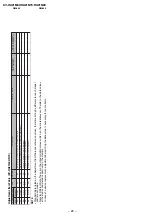
Page 24: ...nt by rewriting the data value is necessary for some items Adjustment Item Table KV HA21N80 N70 y t i l a n o i t c n u F t i n I e g n a R n o i t c n u F e t o N e l b a T o N r e t s i g e R e g n a R t i B e m a N e c i v e D s s e r d d A e v a l S o N e m a N 0 3 A C S 1 0 1 0 f f o n o e l b a C f o n o i t i d n o C g n i p p i h S 1 3 H C S 1 0 F 7 r e b m u N l e n n a h C f o n o i t i ...

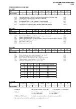
Page 25: ...BB Blue back when no video signal is identified 1 on 0 off 18 0 AKB Black current stabilisation 1 not active 0 active 02 6 BPS Bypass of chroma base band delay line 1 bypassed 0 active 19 6 CB Chroma bandpass centre frequency 1 1 1x Fsc 0 Fsc 18 5 ACL Automatic colour limiting 1 active 0 not active 19 5 CL2 CL1 CL0 Cathode Drive amplitude 0 0 0 57V 0 0 1 63V 0 1 0 70V 0 1 1 77V 1 0 0 84V 1 0 1 91V...

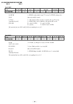
Page 26: ...onal function will be enabled if the corresponding bit is set to 1 No Bal 1 no balance in analog select items 0 balance included for AV stereo model SPC SOUND 1 Space Sound available 0 not available Korean ST Reserved for NTSC model H K Bil 1 NICAM bilingual available No NICAM stereo 0 not available for monaural model Other optional function will be enable if the corresponding bit is set to 1 No 4...

Page 27: ... 0 off 18 0 AKB Black current stabilisation 1 not active 0 active 02 6 BPS Bypass of chroma base band delay line 1 bypassed 0 active 19 6 CB Chroma bandpass centre frequency 1 1 1x Fsc 0 Fsc 18 5 ACL Automatic colour limiting 1 active 0 not active 19 5 CL2 CL1 CL0 Cathode Drive amplitude 0 0 0 57V 0 0 1 63V 0 1 0 70V 0 1 1 77V 1 0 0 84V 1 0 1 91V 1 1 0 99V 1 1 1 107V No 20 VP3 Item KV HA21N70 KV H...

Page 28: ...f the corresponding bit is set to 1 No Bal 1 no balance in analog select items 0 balance included for AV stereo model SPC SOUND 1 Space Sound available 0 not available Korean ST Reserved for NTSC model H K Bil 1 NICAM bilingual available No NICAM stereo 0 not available Multi Model Only Thai Bil Multi Model Only Other optional function will be enable if the corresponding bit is set to 1 No 33 OP2 I...

Page 29: ... and 0 sequentially Read data from NVM push the commander button 7 and 0 sequentially Copy 50Hz data into 60Hz area push the commander button display and 0 sequentially SELF DIAGNOSIS MODE How to enter Self Diagnosis Mode At stand by push the commander button display 5 vol and power sequentially How to exit Self Diagnosis Mode Push the commander button other ON or power AC OFF Other operations Cle...

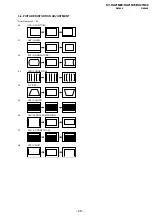
Page 30: ...4 VB1 VB2 VB3 VB4 4 4 DEFLECTION ADJUSTMENT NORMAL MODE 50Hz 1 Set to Service mode 2 Input PAL color bar 3 Using the 1 and 4 button select category GEO Service Mode 4 Raise lower the data using the 3 and 6 buttons Select and adjust the following items to obtain optimum image Service Item GEO 00 HPS H POSITION 01 HSZ H SIZE 02 PAP PIN AMPLITUDE 03 CPN CORNER PIN 04 TLT TILT 05 VSL V SLOPE 06 VAP VE...

Page 31: ...N80 RM 969 RM 968 4 6 PICTURE DISTORTION ADJUSTMENT Item Number 00 08 01 HSZ H SIZE 04 TLT TILT 06 VAP VERTICAL AMPLITUDE 00 HPS H POSITION 02 PAP PIN AMPLITUDE 03 CPN CORNER PIN 05 VSL V SLOPE 08 VPS V SHIFT 07 SCO S CORRECTION ...

Page 32: ... CVBS OUT B Y R Y ABL EHTX RAY IC301 Y C JUNGLE X443 4 43MHz X358 3 58MHz IF OUT CVBS IN INT 6 13 H PROT Q004 Q800 H DRIVE 3 1 PIN CONT IC850 IC851 Q802 PIN OUT IC551 V OUT 5 1 7 Q801 H OUT L802 DUMPER D804 D851 S801 H SENT FV HV 135V 13V 15V T503 FBT Q561 X RAY 135V D561 D591 D1505 H H H H V V DY1 1 5 200V 1000V H1 CN500 CN300 CN703 3 2 1 5 Q712 Q711 Q710 Q706 Q705 Q704 R DRIVE G DRIVE B DRIVE R ...

Page 33: ... 32 KV HA21M80 HA21N70 HA21N80 RM 969 RM 968 5 2 CIRCUIT BOARDS LOCATION A BOARD CV BOARD ...

Page 34: ...N PAL NTSC 3 58 Readings are taken with a 10 MΩ digital multimeter Voltage are dc with respect to ground unless otherwise noted Voltage variations may be noted due to normal produc tion tolerances All voltage are in Volt Cannot be measured Circled numbers are waveform references B bus B bus signal path Reference information RESISTOR RN METAL FILM RC SOLID FPRD NONFLAMMABLE CARBON FUSE NONFLAMMABLE...

Page 35: ... 2k FPRD 100 2W RS 10 FPRD 1 FPRD VOL SEL CH TV VIDEO VOL CH 1 571 433 31 PUB 1 572 707 21 CAS 4HG 3 58MHz 4 43MHz FBI 15MM 220 220 25V JW 5MM SPB 25MVWF 0 0047 500V E 0 47 1 2W FPRD 0 471 2W FPRD 0 47 1 2W FPRD DA204K 8 2M 1W D3SB60F3 AC RECT 0 022 200V PT JW 5MM DA204K PROTECT 220p B CHIP 220p B CHIP RD5 6SB 0 001 B CHIP 0 001 B CHIP 0 001 B CHIP 0 001 B CHIP 0 001 B CHIP 0 001 B CHIP 0 001 B CH...

Page 36: ...1 22UH EL0607 D717 NNCD9 1A T1 C1764 R1774 R711 R713 R715 0 001 B 4 7 250V 0 022 400V PP C706 47 16V 470p B 470p B 470p B 560P B 560P B 100 16V 100 16V 680p B SOCKET 680 RN R707 470 RN 2 2k 2 2k 2 2k 180 180 180 100 100 100 1 2k 1 2k 1 2k JW 5MM JW 5MM JW 5MM 110M 1P TAB 1P TAB C736 0 0047 2kV E 0 68 3W RS R720 JW 5MM JW 5MM JW 5MM 8 2k 3W RS 8 2k 3W RS 8 2k 3W RS 100 1 2W 100k 1 2W 470P B 150 150...

Page 37: ...C217 0 022P 16V CHIP 0 022 16V C218 0 1 16V B CHIP 0 1 16V C219 0 018 16V CHIP 0 018 16V C220 0 022 16V CHIP 0 022 16V C221 0 0047 0 0047 C222 0 018 16V CHIP 0 018 16V C223 0 0047 0 0047 C224 1P 1 C225 1P 1 C226 4 7 4 7 C227 47 16V 4 7 16V C228 1P 1 C229 0 47 0 47 C 230 2 2 6 3V 2 2 6 3V C231 2 2 6 3V 2 2 6 3V C232 2 2 6 3V 2 2 6 3V C238 2 2 C240 2 2 6 3V 2 2 6 3V C241 00082 B CHIP 0 0047 B CHIP 0...

Page 38: ... CHIP 0 CHIP JR202 0 CHIP JR205 0 CHIP 0 CHIP JR213 0 CHIP JR400 0 CHIP 0 CHIP L101 1 2UH L102 0 33UH 0 22UH 0 33UH L103 0 33UH L200 68 47 68 L300 18UH L301 18UH 12UH 18UH L302 8 2UH L303 18UH 8 2UH 18UH L304 12UH L305 12UH L306 1 8UH L307 2 2UH L308 2 2UH L310 27UH Q102 2SC3779C D AA Q103 UN2216 Q104 UN2216 Q106 MSD609 RT1 Q300 MSB709 RT1 Q301 MSB709 RT1 Q303 MSD601 RT1 Q304 MSB709 RT1 Q305 MSB70...

Page 39: ... 2 2K CHIP R313 330 CHIP R314 330 CHIP R315 22K CHIP R317 470 CHIP R318 22K CHIP R319 470 CHIP R320 22K CHIP R323 470 CHIP R338 15K CHIP R352 15K CHIP R356 680 CHIP 3 3K CHIP 3 3K CHIP R393 1 0K CHIP 0 CHIP 0 CHIP R394 7 5K 7 5K R402 100 CHIP 100 R403 10K CHIP 10K CHIP R404 1 0K CHIP 1K R405 10K CHIP 10K CHIP R406 470K CHIP 470K R407 1 0K CHIP 1K R408 1 0K CHIP 1K R419 39K CHIP 39K CHIP R422 56K C...

Page 40: ...101 I 9 G 0 O 0 IC201 1 4 5 2 4 5 3 4 5 4 4 5 5 4 5 6 4 5 7 4 5 8 4 5 9 4 5 10 4 5 11 4 5 12 4 5 13 4 5 14 4 5 15 4 5 16 4 5 17 4 5 18 4 5 19 4 5 20 0 21 4 6 22 4 6 23 4 5 24 9 25 0 26 3 8 27 3 8 28 4 5 IC203 1 0 2 0 3 20 3 4 0 5 0 6 0 7 9 8 8 0 4 9 0 10 21 11 9 7 12 9 7 IC301 1 0 9 1 1 2 3 7 3 0 4 0 5 2 4 3 6 6 2 9 4 4 7 4 6 8 4 5 Ref Pin No Voltage v Ref Pin No Voltage v 9 6 6 10 0 11 3 3 12 8 2...

Page 41: ... C 0 E 0 Q301 B 3 2 4 1 C 0 E 2 4 4 8 Q302 B 0 4 1 C 0 E 3 8 3 6 Q303 B 2 4 4 8 C 7 8 4 8 E 3 0 5 5 Q304 B 3 0 5 8 C 2 4 4 8 E 0 9 Q305 B 2 9 5 8 C 2 3 4 8 E 2 3 9 Q306 B 9 C 9 E 2 9 4 3 Q307 B 9 C 9 E 2 9 4 4 Q308 B 0 C 9 E 0 Q309 B 2 3 9 C 9 E 2 9 0 1 Q310 B 0 C 9 0 E 0 Q311 B 9 3 5 C 9 E 2 9 4 4 Q312 B 0 C 0 9 0 E 3 8 0 Q313 B 0 C 8 9 0 E 0 3 3 Q314 B 0 C 0 E 4 Q315 B 2 7 C 9 E 0 Ref Pin No Vol...

Page 42: ... B 112 104 C 8 E 109 102 Q709 B 111 102 C 8 1 8 3 E 108 100 Q710 B 2 9 C 8 4 E 2 2 2 4 Q711 B 2 7 2 9 C 8 4 E 2 1 2 3 Ref Pin No Voltage v Ref Pin No Voltage v Q712 B 2 8 C 8 4 E 2 1 Q1763 B 133 9 C 68 9 E 134 5 Q1765 B 0 9 C 68 9 E 0 3 Q1767 B 5 5 C 9 E 4 8 Q1777 B 0 7 C 0 E 0 A BOARD VOLTAGE LIST Ref Pin No Voltage v Q924 B 5 5 0 C 9 E 6 1 8 5 Q956 B 0 C 0 E 0 6 Q961 B 1 9 1 4 C 9 2 4 E 2 5 2 1 ...

Page 43: ...p 3 76Vp p 1 2Vp p 3 2Vp p 2 64Vp p 152Vp p 2 92Vp p 4 96Vp p 3 2Vp p 80 8Vp p 1 2Vp p 1 4Vp p 1 12Vp p 416Vp p 3 84Vp p 1 64Vp p 3 16Vp p 420Vp p 4 08Vp p 6 08Vp p 1 2Vp p 2 56Vp p PAL NTSC3 58 1 1 PAL NTSC 3 58 2 PAL NTSC3 58 3 3 PAL NTSC 3 58 4 PAL NTSC3 58 5 PAL NTSC3 58 6 6 PAL NTSC 3 58 7 PAL NTSC3 58 8 PAL NTSC3 58 9 9 PAL NTSC3 58 10 10 PAL NTSC3 58 11 11 PAL NTSC3 58 12 12 PAL NTSC 3 58 1...

Page 44: ... 44 KV HA21M80 HA21N70 HA21N80 RM 969 RM 968 PRINTED WIRING BOARDS 5 6 PRINTED WIRING BOARDS AND PARTS LOCATION CV Board RGB AMPLIFER CV ...

Page 45: ... C411 C341 C340 C304 C339 C337 C330 C328 C327 C313 Q315 C312 C314 D305 D307 C320 C319 C318 C317 C316 Q314 Q407 Q406 C801 IC400 IC401 C112 C104 C105 C334 C336 Q317 Q201 C001 C002 C611 C609 C558 C561 C367 C554 C556 IC850 C856 C858 C860 C859 C625 C122 C121 Q105 C127 Q106 C119 C113 D302 D303 D317 Q001 Q002 D003 D403 D404 D406 D407 D304 C962 C922 C923 C951 C977 C974 C924 D964 D961 D963 D966 D965 Q956 Q...

Page 46: ... T1 RU4AM T3 1SS119 25 D3SB60F3 BY228 UPC574J ANODE CATHODE CATHODE ANODE CATHODE ANODE GRN ANODE GRN TRANSISTOR 2SC2785 HFE E C B LETTER SIDE 2SA1091 0 E C B 2SC2611 E LETTER SIDE C B RN4Z DTC144EKA MSD601 RT1 MSB709 RT1 UN2211 UN2213 UN2216 E B C 2SC3209LK E C B 2SD2624 CA 1 2 3 IC IRF614 005 2SC3779C S D G E B C M24C08 BN6 A 8 PIN CXP85224A 080S 64 PIN CXP85220A 083S 64 PIN TDA7438D013TR 28 PIN...

Page 47: ...21N80 RM 969 RM 968 MM1319AFBE 7 PIN NJM2903M 8 PIN Small Outline L Leaded Pin 8 98 1 TOP VIEW SOP AN5522 TDA8844 TDA8843 STR F6707A Zig zag In line Package Pin 6 99 MARKING SIDE VIEW 1 1 2 4 6 3 5 7 TA7805S SBX3081 21 SE 135N ...

Page 48: ... KV HA21N70 HA21N80 8 4 046 600 11 SPACER DY 9 4 057 714 01 PIECE TLH CONVERGENCE 10 8 451 505 11 DEFLECTION YOKE Y21RSA S 11 A 1332 270 A CV BOARD MOUNTED KV HA21M80 A 1332 200 A CV BOARD MOUNTED KV HA21N70 HA21N80 12 4 057 862 01 SCREW TAPPING 5 CROWN WASHER 13 4 369 318 61 SPRING TENSION KV HA21M80 4 078 765 01 SPRING EXTENSION KV HA21N70 HA21N80 14 1 416 946 11 COIL DEGAUSSING KV HA21M80 1 416...

Page 49: ... 1 162 927 11 CERAMIC CHIP 100PF 5 00 50V C038 1 162 927 11 CERAMIC CHIP 100PF 5 00 50V C039 1 163 038 91 CERAMIC CHIP 0 1UF 25V C041 1 162 924 11 CERAMIC CHIP 56PF 5 00 50V C042 1 162 927 11 CERAMIC CHIP 100PF 5 00 50V C043 1 162 927 11 CERAMIC CHIP 100PF 5 00 50V C044 1 162 924 11 CERAMIC CHIP 56PF 5 00 50V C045 1 126 962 11 ELECT 3 3UF 20 00 63V KV HA21M80 C045 1 126 962 11 ELECT 3 3UF 20 00 50...

Page 50: ...222 1 104 509 11 CERAMIC CHIP 0 018UF 10 00 16V KV HA21M80 HA21N80 C223 1 162 968 11 CERAMIC CHIP 0 0047UF 10 00 50V KV HA21M80 HA21N80 C224 1 126 960 11 ELECT 1PF 20 50V KV HA21M80 HA21N80 C225 1 126 960 11 ELECT 1PF 20 50V KV HA21M80 HA21N80 C226 1 125 805 91 ELECT 4 7UF 20 00 50V KV HA21M80 HA21N80 C227 1 126 947 11 ELECT 47UF 20 00 16V KV HA21M80 HA21N80 C228 1 126 960 11 ELECT 1PF 20 50V KV H...

Page 51: ...1 ELECT 10UF 20 00 50V KV HA21N70 C421 1 126 964 11 ELECT 10UF 20 00 50V KV HA21N70 C422 1 126 964 11 ELECT 10UF 20 00 50V KV HA21N70 C425 1 162 925 11 CERAMIC CHIP 68PF 5 00 50V C426 1 162 925 11 CERAMIC CHIP 68PF 5 00 50V KV HA21M80 HA21N80 C430 1 126 964 11 ELECT 10UF 20 00 50V KV HA21N70 C435 1 126 934 11 ELECT 220UF 20 00 16V C500 1 126 933 11 ELECT 100UF 20 00 16V C501 1 104 666 11 ELECT 220...

Page 52: ... D004 8 719 911 19 1SS119 25 D005 1 162 318 11 CERAMIC 0 001UF 10 00 500V D006 8 719 109 89 RD5 6ESB2 D007 8 719 159 10 RD5 1SB T2 D009 8 719 159 10 RD5 1SB T2 D100 8 719 421 40 MA77 KV HA21M80 D103 8 759 157 40 UPC574J D104 8 719 914 42 DA204K D200 8 719 914 42 DA204K D202 8 719 988 61 1SS355TE 17 D203 8 719 988 61 1SS355TE 17 D301 8 719 988 61 1SS355TE 17 D304 8 719 063 66 HZS361 TE D305 8 719 9...

Page 53: ...4 1 216 295 91 SHORT 0 JR015 1 216 295 91 SHORT 0 JR016 1 216 295 91 SHORT 0 KV HA21M80 HA21N80 JR018 1 216 295 91 SHORT 0 JR020 1 216 295 91 SHORT 0 JR034 1 216 295 91 SHORT 0 KV HA21M80 JR035 1 216 295 91 SHORT 0 JR036 1 216 295 91 SHORT 0 JR100 1 216 295 91 SHORT 0 KV HA21N70 HA21N80 JR202 1 216 295 91 SHORT 0 KV HA21N70 JR205 1 216 295 91 SHORT 0 KV HA21M80 HA21N80 JR210 1 216 295 91 SHORT 0 J...

Page 54: ...R060 1 216 033 00 RES CHIP 220 5 1 10W R061 1 216 033 00 RES CHIP 220 5 1 10W R062 1 216 049 11 RES CHIP 1K 5 1 10W KV HA21M80 R063 1 216 049 11 RES CHIP 1K 5 1 10W KV HA21M80 R064 1 216 049 11 RES CHIP 1K 5 1 10W R065 1 216 049 11 RES CHIP 1K 5 1 10W R066 1 216 049 11 RES CHIP 1K 5 1 10W R072 1 216 065 91 RES CHIP 4 7K 5 1 10W R073 1 216 081 00 RES CHIP 22K 5 1 10W R074 1 216 049 11 RES CHIP 1K 5...

Page 55: ...N80 R202 1 216 089 91 RES CHIP 47K 5 1 10W KV HA21M80 R202 1 216 081 00 RES CHIP 22K 5 1 10W KV HA21N80 R203 1 216 041 00 RES CHIP 470 5 1 10W KV HA21M80 R203 1 216 061 91 RES CHIP 3 3K 5 1 10W KV HA21N80 R203 1 216 051 00 RES CHIP 1 2K 5 1 10W KV HA21N70 R204 1 216 061 91 RES CHIP 3 3K 5 1 10W KV HA21M80 HA21N80 R204 1 216 067 00 RES CHIP 5 6K 5 1 10W KV HA21N70 R205 1 216 081 00 RES CHIP 22K 5 1...

Page 56: ...53 1 216 119 00 RES CHIP 820K 5 1 10W R354 1 216 119 00 RES CHIP 820K 5 1 10W R355 1 216 061 91 RES CHIP 3 3K 5 1 10W R356 1 216 061 91 RES CHIP 3 3K 5 1 10W KV HA21M80 HA21N80 R356 1 216 045 00 RES CHIP 680 5 1 10W KV HA21N70 R357 1 216 101 00 RES CHIP 150K 5 1 10W R358 1 216 025 11 RES CHIP 100 5 1 10W R360 1 216 065 91 RES CHIP 4 7K 5 1 10W R361 1 216 033 00 RES CHIP 220 5 1 10W R362 1 216 083 ...

Page 57: ...AL OXIDE 470 5 3W R602 1 240 262 11 CEMENTED 0 68 5 10W R603 1 240 262 11 CEMENTED 0 68 5 10W R605 1 217 191 21 METAL 0 18 10 2W R606 1 216 045 00 RES CHIP 680 5 1 10W R608 1 260 127 11 CARBON 220K 5 1 2W R609 1 216 091 00 RES CHIP 56K 5 1 10W R610 1 215 926 00 METAL OXIDE 33K 5 3W R611 1 216 067 00 RES CHIP 5 6K 5 1 10W R612 1 249 420 11 CARBON 1 8K 5 1 4W R615 1 215 877 11 METAL OXIDE 22K 5 1W R...

Page 58: ...V C713 1 102 115 00 CERAMIC 560PF 10 00 50V C714 1 102 115 00 CERAMIC 560PF 10 00 50V C716 1 126 933 11 ELECT 100UF 20 00 16V C717 1 102 852 91 CERAMIC 47PF 5 00 50V C718 1 126 933 11 ELECT 100UF 20 00 16V C719 1 102 116 00 CERAMIC 680PF 10 00 50V CLP701 4 042 408 01 PIN COATING LEAD CLP702 4 042 408 01 PIN COATING LEAD CLP703 4 042 408 01 PIN COATING LEAD CLP704 4 042 408 01 PIN COATING LEAD CONN...

Page 59: ...55 1 249 382 11 CARBON 1 2K 5 1 4W R756 1 249 382 11 CARBON 1 2K 5 1 4W R757 1 249 382 11 CARBON 1 2K 5 1 4W VARIABLE RESISTOR RV702 1 241 656 11 RES ADJ METAL FILM 110M ACCESSORIES AND PACKING MATERIALS 1 501 372 81 ANTENNA TELESCOPIC 1 417 170 11 MATCHING TRANSFORMER ANTENNA KV HA21N70 HA21N80 3 701 910 00 SCREW SPECIAL DIA 3 8X20 4 053 003 01 BAG PROTECTION KV HA21M80 4 039 372 01 BAG PROTECTIO...

Page 60: ...872 280 02 English 2002 6 SUPPLEMENT 1 BG2T CHASSIS MODEL COMMANDER DEST CHASSIS NO 17 6 REF NO PART NO DESCRIPTION REMARK 6 X 4039 650 2 COVER ASSY REAR SUBJECT REAR COVER ASSY SUFFIX CHANGE MODEL COMMANDER DEST CHASSIS NO KV HA21M80 RM 969 India SCC U74C A KV HA21N70 RM 968 Philippines SCC U76D A KV HA21N80 RM 968 Philippines SCC U76C A ...

Reviews: