background image

60

27. Grand Wega Lamp Control

+

-

1

3

2

1

2

3

3

12 13

4

5

40

39

50

49

48

IC9502 LAMP

CONTROL

IC9004

MAIN

MICRO

4

4

*

G BD.

A BD.

M BD.

H3 BD.

T BD.

0V

25kV TO GAS

DISCHARGE

LAMP

R1613

N/C

R1654

R1655

F1601

6.3A

POWER
SUPPLY

POWER

S8001

N/C

HV

DET

CN

4502

S DATA

CLK

WIRE

COLOR

WHI GRY

CTL=

ON=5V

OFF=0V

CN1908

CN1901

POWER

BLOCK BD.

PRT

=0V

LAMP COVER
BOARD

270V

CN1602

CN1920/

CN9501

40

LAMP COMES ON

1   WHEN CN1908/PIN 1 = 5V

2   POWER BLOCK BD.
     OUTPUTS 27kV IGNITION
     VOLTAGE , THEN 25kV RUN
     VOLTAGE

TV

BLOCK

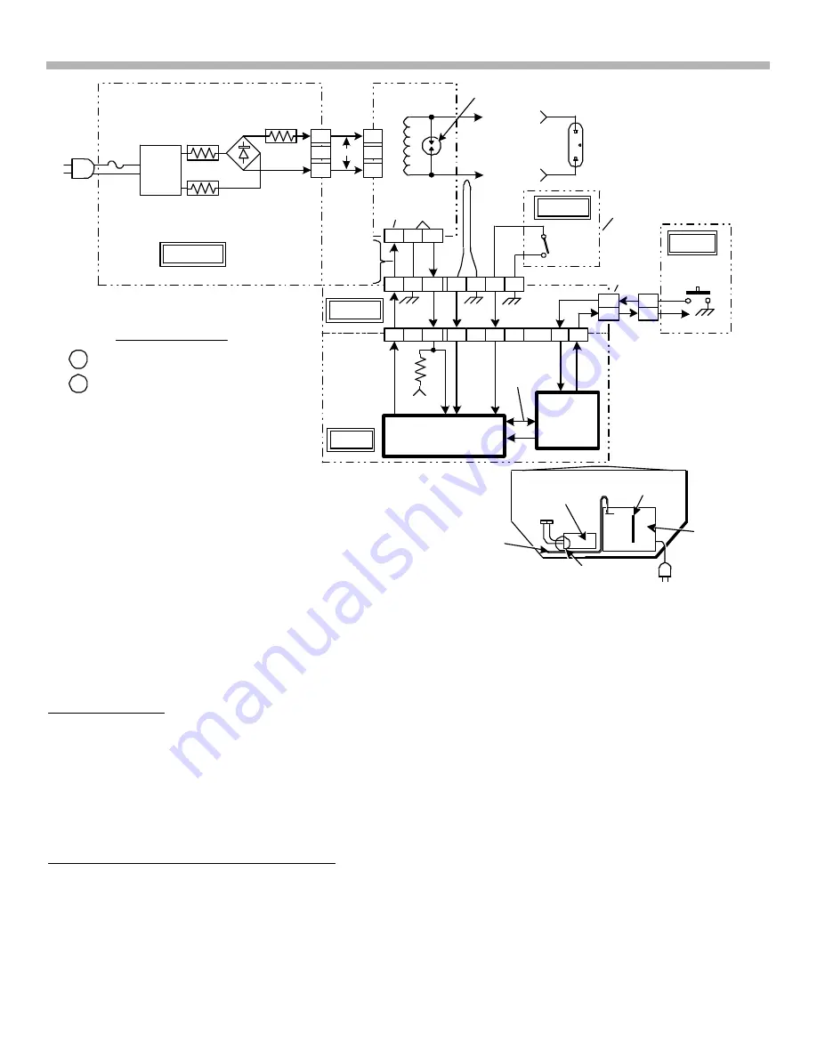
FIGURE 27-1 - LAMP CONTROL - KF-60DX100

M BD.

HV

POWER

BLOCK

HV DET

WIRE

TV FRONT

1

2

6TVP13 1439

4/16/02

45

7

7

STBY LED

LAMP DEFECTIVE -
STBY LED BLINKS CONTINUOUSLY

POWER BLOCK BD. DEFECTIVE -
STBY LED BLINKS 5 TIMES

LAMP COVER SW. OPEN -
STBY LED BLINKS 3 TIMES

MAIN

P.S.

0V

5V

*

255V-

350V

G1

SPARK GAP
G1

New HV Detector Circuit

The purpose of the HV Detector circuit (on the M board) is to identify the cause of no backlight.  The front panels
LEDs use this information.  The LAMP LED blinks continuously if the lamp is defective or the Standby LED will
blink five times if the HV or control circuitry is bad.  Refer to Figure 27-1 for the following HV detector circuit
description:

Normal Operation - At power ON, Main Micro IC9004 instructs Lamp Control IC9502 (both on M board) to output
a HIGH at Ctl (A board, CN1908/pin 1).  This HIGH is applied to the Power Block to start the 25kV necessary for
the lamp ignition.  If the lamp starts to draw current, the Power Block closes the relay to reduce lamp voltage and
grounds the PRT line (CN1908/pin 3 or the end gray wire on the Power Block).

The PRT (protect) line is a signal to tell the Main Micro the lamp is drawing current (working).  When LOW
(0Vdc), the Main Micro in turn unmutes the A/V lines and a picture with sound appears (all within 20 seconds after
turn ON).

Defect - The LAMP LED blinks continuously - The main Micro looks at the PRT signal (CN1908/pin 3) and the
antenna signal to determine if the lamp or Power Block is defective (Table 27-1).  When HV appears without a
load (bad bulb), arcing in the spark gap on the Power Block creates RF that is picked up by the nearby antenna
wire.  This RF signal is brought back to the A board at CN1908/pin 12.  The RF signal only passes through the A
board to get to the M board (CN9501/pin 50) where it is rectified.  On the M board, a DC voltage developed after
the RF signal is rectified indicates the presence of HV (normal Power Block operation).  If there is HV and no
current draw, the conclusion is that the lamp is bad so the Main Micro continuously blinks the front panel LAMP
LED.

Summary of Contents for KZ-32TS1U

Page 1: ...Training Manual Course TVP 13 Plasma TV Grand Wega Projection TV Models KZ 32TS1U KZ 41TS1U KF 60DX100 Diagnostic Guides KZ 32TS1U KF 60DX100 ...

Page 2: ...t 30 12 Video Signal Flow 32 13 What is Flat Screen PlasmaTechnology 35 Theory of Operation 35 KF 60DX100 Introduction 37 15 Normal Operation 38 16 Self Diagnostics 39 17 Board Selection by Defect 40 18 Board Locations 41 19 Adjustments 42 20 Service Mode 44 21 Determining if the Optical Unit is OK 45 22 Optical Unit Removal 46 23 Screen Mirror Replacement 50 24 Troubleshooting TV Shutdown 53 25 P...

Page 3: ...Diagnostics The front panel Standby light blinks to indicate major and minor problems 3 Board Selection by Defect Listing of possible defects and where they may be 4 Plasma Panel picture Defects Listing of possible plasma panel screen defects 5 Board Location Location of replaceable boards in model KZ 32TS1U 6 Service Mode Service Mode access and contents 7 Adjustments Adjustments after the B boar...

Page 4: ...is normal The Main CPU monitors the fan run voltage rotation and ambient temperature of the power supply This information is available to the user from the User Status menu as an OSD on screen display OK or NG indication Details such as the temperature are in the Service Mode see Section 6 Video Inversion to prevent border burn in After a undetermined period of use some plasma cells will not be as...

Page 5: ... screen Cause Suspect Board EEPROM ID check error B board EEPROM read write error B board Color Decoder IC error B board Panel will not initialize start Plasma panel Low B at start up Plasma panel power supply board Table 2 2 Cause of Standby LED Blinking in a Pattern TV Shutdown Times Standby LED blinks Cause Suspected board 2 times Plasma panel error Plasma panel 3 times Internal TV temperature ...

Page 6: ...t for Stby light ON No response to pwr button Plug in relay click heard 2 1 3 Fan not cooling front panel Standby indicator blinking See the TV menu and Fan block diagram in Section 7 Fan NG No voltage to fan Temp NG Fan not working 3 2 1 Noise Bars across the screen horizontal The rear metal shield must contact the conductive mesh on all four sides and be screwed to the center TV board assembly S...

Page 7: ... noise d e f g g A Dark Screen with sound can be caused by the plasma panel or the TV circuitry Measure the DC voltages and signal entering the plasma panel to determine which is defective Power Supply Board CN 23 1 CN 1 13 15 gray wires 1 Dark screen Check DC and signal video levels at CN23 CN 1 Normal Voltages with TV ON any input CN23 pin 1 55Vdc CN23 pin 3 5Vdc CN23 pin 8 10 78Vdc 32 or 82Vdc ...

Page 8: ...6 5 Board Location Chapter 5 Board Location PLASMA BOARD X PLASMA BOARD Y POWER SUPPLY BOARD B BOARD Q BOARD VHF IN TU BD FIGURE 5 1 BOARD LOCATION KZ 32TS1U 8TVP13 1444 4 10 02 ...

Page 9: ... the TV is OFF Standby sleep light TV Figure 6 1 2 Using a Sony remote control aimed at the TV in the standby mode quickly press Display 5 Volume Power ON and MENU If the TV turned ON when 5 was pressed you did not press the next Volume button fast enough and will have to try again 3 The following new service Mode menu shown in Figure 6 2 will appear above the user menu Use the remote control joys...

Page 10: ...settings to default except diagnostics and serial number Tuner Micom Same as Tuner Chroma Decoder See Figure 6 4 for a content list Preset contrast sharpness color and output levels as shown in Figure 6 4 The Hue for NTSC 8 Y Delay 8 and Cb Cr Offset 8 Sharp fo is the frequency the sharpness peaks 0 2 5M 1 3 2M 2 4M 3 off Set to 3 AD Converter Adjust the brightness and hue for each input video com...

Page 11: ...ns from the Main Micro B board to memory IC and to 15 others Operation Time Elapse TV ON time Software PLD version Software in Main micro and Panel Micro Table 6 2 Service Mode Service Status under Fan and Temp No Acknowledge Device Defect Code Suspected IC Defect Code Suspected IC 0001 Audio Processor A board 0002 Audio Switch Q board 0004 AV Switch IC U board 0008 V Chip Q board 0010 3D Comb fil...

Page 12: ...10 6 Service Mode Figure 6 4 Service Mode Chroma Decoder Figure 6 5 Service Mode General Figure 6 6 Service Mode Manual Control 1 2 ...

Page 13: ...11 6 Service Mode Figure 6 7 Service Mode Manual Control 2 2 Figure 6 8 Service Mode Preset Edit Figure 6 9 Service Mode Service Status ...

Page 14: ...igure 7 1 2 Using a Sony remote control aimed at the TV in the standby mode press Display 5 Volume Power ON and MENU quickly If the TV turned ON when 5 was pressed you did not press the next Volume button fast enough and will have to try again 3 The following new service Mode menu shown in figure 7 2 will appear above the normal user menu Use the remote control joystick to move and change the data...

Page 15: ...ideo Video Composite Video Item 32 Level 42 Level Item Level 42 Level Item Level 42 Level Sub Cont RGB 104 110 SubCont YUV 102 106 SubCont Video 68 65 Red Gain 100 114 Sub Bri YUV 146 145 SubBrt Video 150 142 Green Gain 128 128 Cb Offset YUV 30 31 Cb Offset Video 32 34 Blue Gain 129 131 Cr Offset YUV 31 31 Cr Offset Video 32 34 Red Bias 142 139 Green Bias 148 147 Blue Bias 150 150 ...

Page 16: ...m low to middle to high screen brightness The white areas of the picture should remain white even as the brightness is changed If the white balance is off return to the stop service mode and touch up the R G or B adjustment level KZ32TS1U Figure 7 4 shows the White Balance levels from a 32 Plasma TV White Balance Color Temp Mid R G B X X X White Balance Color Temp Low R G B X X X White Balance Col...

Page 17: ...there are flex cables located at the bottom and both sides of the panel that are susceptible to damage So the flex cables are not damaged only rest the plasma panel topside down as shown in figure 8 1 Bottom Flex Cables Panel Bottom Top Figure 8 1 Plasma Panel Standing Upside Down Flex Cables Procedure KZ32TS1U In the steps to follow you will remove the rear panel the shield the board assembly and...

Page 18: ...Remove Figure 8 2 Back Removed a Begin by removing the back panel to expose the shield shown in figure 8 2 b Unplug the fan and remove the shield Lower Board Assembly Board Layout TV Board Assembly Plasma Panel Power Supply Board Figure 8 3 Circuit Boards ...

Page 19: ...sembly held in by four black screws Two can be easily seen at the right in Figure 8 5 The left two are behind the plate In the next three steps you will lower the front Q board to remove all the screws and pull out the H1 board cable harness from the assembly d Remove two screws holding the front Q board in the TV board assembly see Figure 8 5 Fold it down e Remove the four black screws holding th...

Page 20: ...igure 8 6 Remove TV Board Assembly 2 In the next two steps the TV must be supported while face down and the base removed Ÿ Insert Books Phone Book s Phone Book s Figure 8 7 Base Removal 1 g Lay the TV face down on a clean soft cloth Bubble wrap was used in these pictures because it was clean and soft h Use books to lift the base off the floor ...

Page 21: ...2TS1U Bezel P S and Plasma Screen Ÿ Remove bracket Support Brackets Figure 8 9 Base Removal 2 i Remove the base j Lay the TV screen flat on the floor Top View Support Brackets Figure 8 8 Base Removal 1 k Remove the two support brackets ...

Page 22: ...ove the plasma screen use the four black handles to lift Only place the top of the plasma screen down The other three sides have vulnerable flex cables present Bottom Flex Cables Panel Bottom Top Figure 8 11 Plasma Panel Standing Upside Down Flex Cables m Remove the power supply board mounted on the larger metal heat sink ...

Page 23: ...ug in the connectors Make sure these test connectors on the B and Q boards are empty Figure 8 13 shows the location of empty CN1003 CN1002 CN1201 and CN3008 Figure 8 13 Unused Test Connectors B Board CN1003 CN1002 CN1201 Q Board CN3008 n The inside of the TV screen is coated so do not clean or leave oil on it by touching it The inside surface scratches easily Clean the inside of the TV screen if t...

Page 24: ...es without the fan connected There will be horizontal noise bars of interference from the power supply when the rear shield is not installed Install the TV shield and fan Make sure the shield makes contact to the conductive mesh on all four sides and the shield is screwed into the center TV board assembly or you will have interference on the TV stations Fan Shield Figure 8 2 Install the rear panel...

Page 25: ...s of the panel that are susceptible to damage Only rest the plasma panel topside down so the cables are not damaged The 32 Plasma panel is shown The 42 is similar Bottom Flex Cables Panel Bottom Top Figure 9 1 Plasma Panel Standing Upside Down Flex Cables Procedure In the following pictured steps you will remove the rear circuit board assembly and the rear shield Before you can pull off the plasma...

Page 26: ...ribbon cable Figure 9 3 by pulling it straight out Do not fold the ribbon cable FIGURE 9 3 REMOVE 7 CONNECTORS AND 7 SCREWS Unplug Connector 7 Machine Screws Squeeze Connector Pull Catch Connector Squeeze Connector Ribbon Cable behind the tape Circuit Board Assembly c Remove the seven machine screws around the circuit board assembly and pull off the assembly d Remove the rear shield with the top d...

Page 27: ...onductive Mesh Tape Conductive Mesh Tape Handles g Mark the position of the conductive mesh tape around the plasma panel before removing them They are necessary to prevent interference on the screen h With a partner lift the plasma screen off by the handles Figure 9 6 PLACE THE PANEL UPSIDE DOWN ON THE FLOOR SEE FIGURE 9 7 The power supply board must be removed from the panel if the panel is to be...

Page 28: ...V screen if there is film or fingerprints Use the Sony p n X 4034 197 1 soft cloth and diluted mild window cleaner if necessary A 50 mix of water and window cleaner is OK Do not use dishwashing detergent or soaps Place the screen in the bezel Mount the rails B board and stand Plug in four connectors from the B board into the plasma panel as shown in Figure 9 8 CN9004 next to connector 2 is not use...

Page 29: ... the TV channels from the power supply After testing remove the rear circuit board assembly to install the shield Install the rear shield with the decorative top control panel Put the top ferrite assembly inside the shield or you will not be able to fasten the rear cover later on Make sure the shield mates with the metal on all four sides to complete the shield Attach the rear circuit board assemb...

Page 30: ... passes through C16 into the standby power supply circuit Within the standby power supply is IC10 and T1 IC10 is an oscillator that starts and feeds small transformer T1 T1 outputs standby 5Vdc to the Micro CPU B board and standby 3 3Vdc to the plasma panel Another T1 output not shown supplies voltage to the end of C16 to keep the standby power supply ON after the kick start pulse had decayed Ther...

Page 31: ...ands are VSA_GO and VCE_GO from CN 7 pins 6 and 8 When both of these two commands go HIGH the power supply outputs the remainder of the voltages and the TV turns ON Within the power supply board three separate regulated supplies reside PS1 PS2 and PS3 As shown in Figure 10 2 these power supplies feed output transformers T4 T5 and T2 respectively T4 outputs the Vs sustain driver voltage and T5 outp...

Page 32: ...005 13V CN7 CPU_GO CN1 CN1203 FAN DET FAN FB CN3003 CN1001 CN2 RDP_GO FIGURE 11 1 FAN DRIVE 2TVP13 1432 4 16 02 Q BD 4 ROTATION 0V THERMO THERMO 5V CN1 0V 0 C 0 8V 21 C 4 7V 100 C 0V 8 6V TV SHUTS DOWN WHEN CN1 PIN4 RISES TO 4 3V 32 92 C 3 76V 42 80 C PLASMA PANEL B BD POWER SUPPLY BD 6 5 7 5V 18k 5V Fan Drive Voltage When the TV is turned ON the Main CPU B board outputs 5Vdc CN1001 pin 24 to the ...

Page 33: ... DVM 4 Is CN3005 pin 1 0Vdc Replace the power supply board 5 Is CN1001 pin 24 at 0Vdc or stays at 5Vdc at power ON 5Vdc at CN1001 pin 24 during power ON means the B board is OK so the Q board is bad 0Vdc at CN1001 pin 24 during power ON means the B board is bad Replace the B board Testing the fan The fan should be tested by applying voltage to it Voltage Test The fan starts running when 6Vdc is ap...

Page 34: ...NENT VIDEO Y R Y B Y Y Cr Cb S VIDEO COMPOSITE VIDEO SYNC H V C Y VIDEO R Y Y B Y Cr Y Cb H V CN1204 CN1 CN102 CN3004 CN3001 CN3002 CN401 HD15 VGA PLASMA DISPLAY PANEL OUT 0 OUT 1 OUT 2 CLK OUT OUT 3 H V FIGURE 12 1 VIDEO SIGNAL FLOW 3TVP13 1433 4 12 02 TU BOARD B BOARD Q BOARD 5 4 7 5 7 6 11 9 9 8 15 13 11 10 19 17 Signal Levels The tuner signal levels Table 12 1 were taken with an NTSC generator...

Page 35: ...pin 13 15 Gray 0 7Vp p Out 3 CN1204 pin 10 11 CN 1 pin 17 19 White 0 7Vp p The main digital signal level is shown but there are ten spikes of power supply noise in the body of the waveshape that are not shown bringing the signal level to 6Vp p The noise is also present on the TV screen when the rear shield is not installed FIGURE 12 2 DIGITAL VIDEO OUTPUT WAVESHAPES TO THE PLASMA PANEL Signal Name...

Page 36: ... digital video signal is accompanied by a clock signal for timing Missing Clock signals CLK Out produce a dark screen no picture with normal sound Missing LSB signals Out 0 or Out 1 produce a picture without detail as shown in figure 12 4 FIGURE 12 4 TV Picture missing Out 0 or Out 1 LSB Picture Detail TV Picture missing Out 0 or Out 1 LSB picture detail Splotches appear on faces or areas where th...

Page 37: ... During ionization an orange glow around the negative electrode is produced Both electrodes appear to glow if AC is applied Varying the current that is allowed to flow by changing the external series resistance through the bulb controls the brightness Cell Structure Refer to Figure 13 1 for the plasma cell structure In a plasma cell plasma replaces the neon gas in the tube Plasma is a collection o...

Page 38: ...as shown in Figure 13 2 1 2 3 4 5 6 7 8 16 9 FIGURE 13 2 SONY 16 X 9 PLASMA PANEL SEGMENTS Cell Intensity Screen Brightness The intensity of the cell is determined not by how bright it glows but by how often it fires within a field or frame The more times it fires the brighter the cell seems but actually they fire at full intensity each time The number of times it fires is based upon the phosphor ...

Page 39: ...fects and related boards by probability 18 Board Location Picture of the boards in the TV 19 Adjustments Video adjustments when changing the BB BC or M board No convergence adjustments 20 Service Mode Access and new contents 21 Determining if the Optical Unit is OK Symptoms are Shutdown white or black screen or missing color 22 Optical Unit Removal Pictured steps 23 Screen Mirror Replacement The e...

Page 40: ...s later a lamp relay on the lamp board will click to move to toward the second brightness level After the lamp relay clicks the lamp will take a minute to gradually reach almost full brightness Lamp Remains ON Although the audio and video is muted immediately at turn OFF the TV remains on for five seconds afterwards During these five seconds the lamp steps to a lower brightness while the fans cont...

Page 41: ... Block board or the Lamp 6 times Low or missing 5Vdc G board or a load on the 5V line any board If the problem is not on the G board unplug each board then power ON the TV to see if 5Vdc appears at CN1604 pin 1 Remove the BB board first 9 times L R Audio Output speaker line monitored for 0Vdc G board power supply or A board audio output Check 15Vdc fuses PS1601 1602 on G board This self diagnostic...

Page 42: ...uses PS1601 2 Dark Screen sound OK 3 2 1 4 See Determining if the optical unit is OK for quick tests Dead Set no relays heard 1 also ck for open BiMetal fuse under rear fan Dead Set relays click See Standby indicator blinks Stby LED blinks 3 times 1 Ck lamp cover Sw 2 M Bd Stby LED blinks 4 times 1 Fan 2 A Bd 3 Stby LED blinks 5 times 1 2 Stby LED blinks 6 times 3 2 5 4 1 6 Stby LED blinks 9 times...

Page 43: ... KZ 41TS1U TV Diagnostic Guide Chapter 18 Board Locations FIGURE 18 1 BOARD LOCATIONS Power Block Lamp Power Supply Optical Unit Bottom A Board BB Board BC Board M Board U Board G Board Power Supply FIGURE 18 2 BOARD LOCATION ...

Page 44: ...tortion inspect the mirror top area of the TV for damage Convergence Convergence is not adjusted in this set The LCD panels are positioned at the factory for convergence Figure 19 1 shows a crosshatch pattern If convergence is off the top mirror assembly and the optical unit where the LCD panels are located are both suspect If the misconvergence is on one side of the screen accompanied by geometri...

Page 45: ... First adj red dots with a Red field then Green and finally Blue You must be at the screen to see the even vs odd dots Section 3 5 page 43 Section 3 3 page 42 A board Picture Adjustments RF video and component inputs are adjusted for consistent white level and color Section 3 2 page 39 BB board Same as above Section 3 2 page 39 BC board Same as above except component video levels need not be adjus...

Page 46: ... Description Typical Data 0 Lamp Time Lamp operating time in hours Hours shown when data is changed to 1 Reset when data 0 is stored mute enter 0 1 Lamp Off Lamp time after TV turns OFF 0 0sec 1 5 seconds 1 2 Fan Off Fan time after TV turns OFF 0 0 mins 1 2 mins 0 3 Fan 1 RPM 1 LCD Fan speed TV ON 3 speeds 0 slow 2 4 Fan 1 RPM 2 LCD Fan speed after TV is OFF 3 speeds 2 5 Fan 2 RPM 1 Lamp Fan speed...

Page 47: ... problem with another IC a fan defect a lamp circuit defect or an audio output failure which may also cause TV shutdown but not a video failure If the screen is white there may be no input to the optical unit Check for loss of input voltage at CN5002 and RGB input signal at CN5005 If the input voltages and signals are present the optical unit is suspect Table 21 1 Optical Unit Input Voltages and S...

Page 48: ...the C board The optical unit is held in with just two screws but the TV board assembly and the power block board must be pulled out to access these screws The optical unit is replaced as an assembly Procedure a Remove the lower back panel and the three support brackets Figure 22 1 FIGURE 22 1 THREE SUPPORT BRACKETS b Lift the TV board assembly up and outward Figure 22 2 ...

Page 49: ...holding the lamp socket Figure 22 3 The power block HV wires are not long enough to permit the power block to swing out of the way Power Block Assembly HV Lamp Socket Power Block Lamp Driver Board FIGURE 22 3 REMOVE TWO HV LAMPSOCKET SCREWS d Lift the Lamp board assembly up and outward figure 22 4 ...

Page 50: ...R BLOCK UP AND OUT e Loosen the two screws under the optical unit Figure 22 5 The screws are part of the optical unit Optical Unit Assembly Screen TV Assembly Power Block Board FIGURE 22 5 OPTICAL UNIT SCREWS EXPOSED f Slide out the optical unit ...

Page 51: ...val Lamp Power Block Assembly Optical Unit Assembly Lens TV Board Assembly FIGURE 22 6 OPTICAL UNIT ASSEMBLY g Dust the optical unit lens with a soft cloth before installing Specks of dirt are magnified so clean it carefully ...

Page 52: ...enter Support Bracket 4 Top Assembly Screws FIGURE 23 1 REMOVE THE REAR CENTER SUPPORT BRACKET AND SCREWS c Also from the back remove the four screws securing the top assembly to the lower electronics Figure 23 1 d Refer to Figure 23 2 From the front of the TV pull the two side panels off to expose the control panel screws e Remove the top two screws of the control panel and loosen the remaining f...

Page 53: ...NTROL PANEL f From the front remove the remaining four screws Figure 23 3 4 Screws FIGURE 23 3 REMOVE THE TOP FOUR SCREWS g With the help of another person lift the top assembly off Do not leave the glass mirror in the top assembly exposed to dust and children Clean the lens with a soft cloth Figure 23 4 before installing the top assembly ...

Page 54: ...52 23 Screen Mirror Replacement Lens FIGURE 23 4 BOTTOM TV BASE ...

Page 55: ... G board defective CN1605 pin 5 0Vdc M or A board is bad Measure CN1921 pin 21 at power ON CN1921 is under the TV board assembly 0vdc M board bad 5Vdc A board bad Normal CN1605 pin 4 7Vdc CN1605 pin 5 5Vdc G board bad or Sw bad START POWER ON Standby LED indicator blinking Stby LED blinks 3 times Lamp cover sw 4 times Fan A G M board 5 times Lamp board 6 times G board 9 times G or A board Relays C...

Page 56: ...the bottom A board where it is regulated down to 5Vdc and passed onto the Main Micro on the M board via CN1921 pin 16 IC9004 MAIN MICRO IC1905 REG MAIN POWER SUPPLY STANDBY POWER SUPPLY 3 1 4 2 5 1 3 1 Q1603 ERROR REG 1 2 2 6 1 2 3 4 1 2 3 4 3 7 5 47 45 16 48 IR STBY 5V STBY LED 21 POWER SIRCS STBY LED STBY 5V PWR ON POWER PWR RELAY RY1601 0 2Ω 0 5Ω STBY 5V F1601 6 3A R1627 22 1W PS1601 PS1602 CN ...

Page 57: ...asses through the A board into the power supply G board at CN1605 pin 5 5Vdc 4 If the Bi metal fuse under the lamp fan 2 is closed CN1614 pin 1 3 connected then the power ON command into CN1605 pin 5 5Vdc can energize the power relay RY1601 on the A board 5 Within the G board power relay RY1601 contacts close passing AC to the Main power supply The Main power supply outputs various voltages to pow...

Page 58: ... temperature of the lamp assembly reaches a critical level the TV will also turn OFF A replaceable Bi Metal fuse located under fan 2 lamp cooling will open if the lamp assembly gets excessively hot Fan Drive Refer to Figure 26 1 The power supply board s 11Vdc CN1613 pin 1 4 source powers both fans In between the power supply and fan is the A board On the A board is regulator IC1908 that provides s...

Page 59: ... 2 3 4 5 4 4 5 1 CN1614 21 16 26 20 21 18 19 23 45 6 5 7 9 8 10 7 3 7 3 22 FIGURE 26 2 FAN CONTROL KF 60DX100 11V CN1604 CN1926 9V 7TVP13 1442 4 16 02 H3 BD A BD PWR SUPPLY BD RY 1601 5V FAN 1 FAN 2 BI METAL PS BD M BD CN1908 TV REAR A BD FAN BOARD LOCATION 7V Fan Rotation Detection When drive voltage to the fan is present the fan rotation detector output will ground out the 5Vdc input at CN1908 p...

Page 60: ...and 9 5Vdc and 9Vdc respectively at power ON If both voltages are present the fans should be rotating Replace the fan if there is voltage but no rotation 3 With the fan rotating there should be 0Vdc at CN1908 pin 8 and 10 If either is 5Vdc replace the corresponding fan see Figure 26 2 At this time fan 1 is part of the light box optical assembly and not available separately 4 There should be 0Vdc e...

Page 61: ...d voltage is reduced across its terminals Not only is the applied voltage reduced when current is drawn Power Block relay clicks but the voltage across the tube lamp drops because the tube s resistance has dropped at ignition like a fluorescent tube The Power Block voltage reduction relay clicks one second after the lamp ignites The phosphor that coats the tube takes about one minute to glow at a ...

Page 62: ...Operation At power ON Main Micro IC9004 instructs Lamp Control IC9502 both on M board to output a HIGH at Ctl A board CN1908 pin 1 This HIGH is applied to the Power Block to start the 25kV necessary for the lamp ignition If the lamp starts to draw current the Power Block closes the relay to reduce lamp voltage and grounds the PRT line CN1908 pin 3 or the end gray wire on the Power Block The PRT pr...

Page 63: ...at end gray wire CN1908 pin 3 the lamp or the Power Block is defective To determine which is defective the antenna signal explained in the last paragraph is used by the Main Micro only when the PRT line CN1908 pin 3 remains HIGH no lamp current During this defect PRT HIGH forces the Main Micro IC9004 to request information about the presence of HV via serial data from Lamp Control IC1952 If RF HV ...

Page 64: ...ove return to step 3 Lamp Time item but change the data to 0 and press MUTE then Enter The hours will reset to 000 3 Power Block Location Removal From the back of the TV set the Power Block is located at the bottom center Figure 27 3 shows the Power Block right and its HV wires terminated at the lamp socket left Power Block Assembly HV Lamp Socket Power Block FIGURE 27 3 HV LAMP CONNECTOR The Powe...

Page 65: ...mb to 25kV and arc across the spark gap device G1 on the Powre block proving the Power Block and controlling M board are working The HV arcing makes an audible frying sound and light is visible The HV arcing lasts two seconds stops for five seconds and repeats until the TV shuts down in three minutes Troubleshooting procedure If the Power Block arcs the bulb is either defective or not plugged in N...

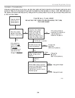
Page 66: ...sible Watch the G1 spark gap behind C101 Turn ON the TV Do you hear a HV frying noise or see light from the G1 body WARNING At TV turn ON LETHAL HV at high current unliked an FBT outputs the Power Block Observe spark gap cylinder G1 for HV from two feet away or more Close front panel lamp door so HV can start Does Ctl white wire change to 5Vdc at TV turn ON Is there 255 350 Vdc Across the Power Bl...

Page 67: ...outputs COMPOSITE VIDEO V TV OUT V COMPONENT VIDEO R Cr Cb A20 C20 A29 C29 A15 A16 A17 C12 A13 C14 C7 C6 C30 C31 C10 C9 C8 C13 C12 C11 C1 1 15 3 5 IC2004 A V SW 3D COMB FILTER IC3009 CCD C20 C22 C21 C29 C27 C28 TUNER IC3004 YCT CCD IC3006 YCT SEL IC3011 MILD SEL 20 24 22 40 36 38 IC304 DRC IC509 MID IC701 RGB DECODER LCD PANEL S VIDEO Y C MAIN CN1923 CN704 Y Cb Cr Cr Cb Y OSD FROM M BD VIDEO SYNC ...

Page 68: ...e groups White Screen Video path open on any video signal board Black Screen BB board or optical unit are suspect Video Screen Distortion Narrow down by checking the features In a conventional TV a loss of video signal results in a white screen with normal TV sound This is also true in this LCD projection TV However if the screen is dark with normal sound either the LCD optical unit or the previou...

Page 69: ...04 S Data white Video Screen Distortion Distortion defects or interference can enter the video chain at any of its five boards used in the video processing chain You can use some features to help determine where the video problem is The features most helpful in isolation are the On Screen Display OSD menu the MILD picture mode activity in Video 5 6 inputs and the Twin View Mode On Screen Display t...

Page 70: ...reation Circuitry feeding it directly into the MID IC Noisy NTSC input signals can fool the DRC circuit into introducing false picture improvements adding to the noise making the MILD mode useful with noisy signals Using Twin View Mode to Locate the Video Problem Twin View Signal Path Concept This TV has the ability to display two pictures side by side on the same screen In the Twin View picture m...

Page 71: ...B board When the picture on the LEFT becomes the larger Figure 28 4c the Main and Sub input signals switch BC board and the MID process IC509 BB board also switches the picture position This double signal crossing allows the channels to be at the same place on the screen but the signal paths are different This switching is done to ensure the high quality DRC signal is employed by the larger pictur...

Page 72: ...oard If the problem is in component video change the BC board Press the Twin Mode button on the remote control and make the RIGHT picture larger Does the problem remian where it is on the screen Do both pictures have the same problem Make the LEFT picture larger Where is the defect BC and BC4 boards are both suspect Unplug the BC4 board and jump the A board s CN1901 pin 1 to pins 3 and 5 Problem g...

Page 73: ...Sony Electronics Inc EMCS A Service Company 1 Sony Drive Park Ridge New Jersey 07656 All Rights Reserved 2002 TVP130402 04 22 02 is a trademark of Sony Electronics ...

Reviews: