— 99 —
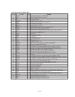
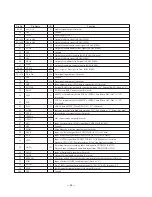
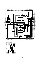
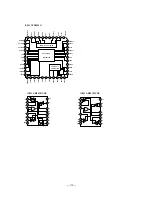
• IC409 Sampling Rate Converter (CXD8517Q)
Data input
Input data fs word clock input (Schemidt)
Input data bit clock input
Input data format setting input 0 (Fixed at “L”)
Input data format setting input 1 (Fixed at “L”)
+5V power supply
Input data fs reference clock input (512fs, 384fs, 256fs, 128fs)
Output data format setting input 0 (Fixed at “L”)
Output data format setting input 1 (Fixed at “L”)
Initializing input (Schmidt). “L”: Initializing, “H”: Normal operation
Not used
Ground
Inverter input for oscillating the crystal oscillator (512fo master clock input)
Inverter output for oscillating the crystal oscillator (Not used)
+5V power supply
Oscillation clock division output: 256fs (Not used)
Ground
Input data through output mode setting input. “L”: Normal operation, “H”: Through
(When through: Effective operation output only for deemphasis, attenuation) (Fixed at “L”)
FI128 clock input division ratio setting input (Fixed at “L”)
FI128 clock input division ratio setting input (Fixed at “L”)
Test input 0 (Not used)
Not used
Test input 1 (Fixed at “L”)
Test input 2 (Fixed at “L”)
Test input 3 (Fixed at “L”)
fs conversion ratio measurement condition monitor output (Not used)
+5V power supply
Not used
Data output (fso output)
Output data bit clock input/output
Output data fs word clock input/output
Not used
Data output mute setting input. “L”: Mute, “H”: Normal operation
Synchronized with LRCK (“0" data only for DATAO output) (Fixed at “H”)
Deemphasis setting input. “L”: OFF, “H”: ON (Fixed at “L”)
Deemphasis setting output fso frequency selection input 1 (Fixed at “L”)
Deemphasis setting output fso frequency selection input 2 (Fixed at “L”)
Ground
Attenuation, mode setting data latch pulse input
Attenuation, mode setting clock input
Attenuation, mode setting data input
Sync mode selection. “L”: Slave, “H”: Master (Fixed at “L”)
Not used
1
2
3
4
5
6
7
8
9
10
11
12
13
14
15
16
17
18
19
20
21
22
23
24
25
26
27
28
29
30
31
32
33
34
35
36
37
38
39
40
41
42
43
44
DATAI
LRCKI
BCKI
MI0
MI1
VDD
FI128
MO0
MO1
INIT
NC
GND
XI
XO
VDD
XO2
GND
PASS
FIS0
FIS1
TEST
NC
NC
TEST1
TEST2
TEST3
STA
VDD
NC
DATAO
BCKO
LRCKO
NC
NC
MUTE
DEMP
FS1
FS2
GND
XLAT
SCK
SWDT
SLAVE
NC
I
I
I
I
I
—
I
I
I
I
—
—
I
O
—
O
—
I
I
I
O
—
—
I
I
I
O
—
—
O
I/O
I/O
—
—
I
I
I
I
—
I
I
I
I
—
Function
I/O
Pin No.
Pin Name
Summary of Contents for MDS-B5
Page 2: ... 2 ...
Page 5: ... 5 SECTION 1 GENERAL This section is extracted from instruction manual ...
Page 6: ... 6 ...
Page 7: ... 7 ...
Page 8: ... 8 ...
Page 9: ... 9 ...
Page 10: ... 10 ...
Page 11: ... 11 ...
Page 12: ... 12 ...
Page 13: ... 13 ...
Page 14: ... 14 ...
Page 15: ... 15 ...
Page 16: ... 16 ...
Page 17: ... 17 ...
Page 18: ... 18 ...
Page 19: ... 19 ...
Page 20: ... 20 ...
Page 21: ... 21 ...
Page 22: ... 22 ...
Page 23: ... 23 ...
Page 24: ... 24 ...
Page 25: ... 25 ...
Page 26: ... 26 ...
Page 27: ... 27 ...
Page 28: ... 28 ...
Page 29: ... 29 ...
Page 30: ... 30 ...
Page 31: ... 31 ...
Page 32: ... 32 ...
Page 49: ......
Page 50: ......
Page 51: ......
Page 52: ......
Page 53: ......
Page 54: ......
Page 55: ......
Page 56: ......
Page 57: ......
Page 58: ......


