background image

– 9 –

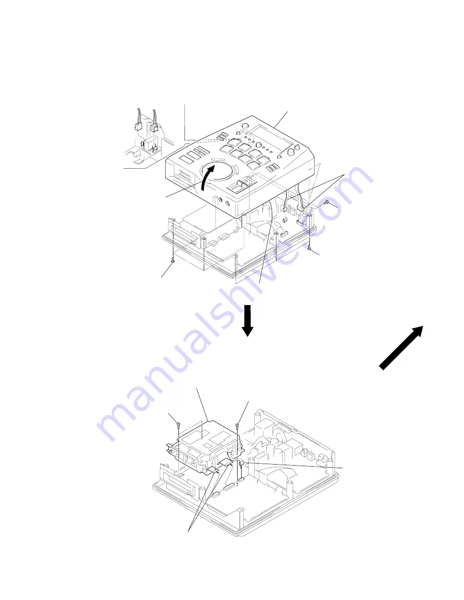
UPPER  CABINET  SECTION

MD  ASSEMBLY

Note:

 Follow the disassembly procedure in the numerical order given.

SECTION  3

DISASSEMBLY

4

two connectors
(CN801, 802)

3

Open the upper cabinet
section in arrow direction.

1

five screws
(BV3 

× 

10)

1

three screws
(BV3 

× 

10)

2

two screws
(BV3 

× 

8)

6

upper cabinet section

4

two connectors
(CN701, 751)

5

flat wire
(CN902)

3

two screws
(BVTP3 

×

 8)

2

two flat wires
(CN4, 5)

3

two screws
(BVTP3 

×

 8)

1

connector
(CN3)

4

MD assembly

Summary of Contents for MDS-DRE1

Page 1: ...l AEP Model UK Model SPECIFICATIONS MDS DRE1 U S and foreign patents licensed form Dolby Laboratories Licensing Corporation Model Name Using Similar Mechanism MDS JA3ES MD Mechanism Type MDM 2CR Base Unit Name MBU 2B Optical Pick up Name KMS 210A J N Continued on next page ...

Page 2: ...m MAIN Section 2 2 25 6 4 Block Diagram DISPLAY KEY POWER SUPPLY Section 27 6 5 Notes for Printed Wiring Board and Schematic Diagram 30 6 6 Printed Wiring Board BD Board SIDE A 31 6 7 Printed Wiring Board BD Board SIDE B 33 6 8 Schematic Diagram BD Section 1 2 35 6 9 Schematic Diagram BD Section 2 2 37 6 10 Printed Wiring Boards DETECTION SW Board MOTOR Board 39 6 11 Schematic Diagram DETECTION SW...

Page 3: ...fte av batteri Benytt samme batteritype eller en tilsvarende type anbefalt av apparatfabrikanten Brukte batterier kasseres i henhold til fabrikantens instruksjoner VARNING Explosionsfara vid felaktigt batteribyte Använd samma batterityp eller en likvärdig typ som rekommenderas av apparattillverkaren Kassera använt batteri enligt gällande föreskrifter VAROITUS Paristo voi räjähtää jos se on virheel...

Page 4: ... a disconnected chip component Notice that the minus side of a tantalum capacitor may be dam aged by heat CAUTION Use of controls or adjustments or performance of procedures other than those specified herein may result in hazardous ra diation exposure This appliance is classified as a CLASS 1 LASER product The CLASS 1 LASER PRODUCT MARKING is located on the rear exterior Laser component in this pr...

Page 5: ... tube This is useful for locating the faulty part of the unit The retry cause number of retries and number of retry errors are displayed Each is displayed in hexadecimal number Method 1 Load a recordable disc whose contents can be erased into the unit 2 Press the STOP button EJECT button PAD1 button simultaneously 3 Press the REC button and start recording 4 The value increases with each retry If ...

Page 6: ...he PLAYBACK MODE is set The display becomes as shown in Fig 2 The playback mode is not used in particular during servicing 44 p Fig 2 Display during Playback Mode 4 Parts No Name of area named on TOC Address Physical address on disc p Track mode Copyright information of each part information on copyright etc Hexadecimal Bit Binary Higher Bits Lower Bits 8 4 2 1 8 4 2 1 b7 b6 b5 b4 b3 b2 b1 b0 0 0 ...

Page 7: ... 7 SECTION 2 GENERAL NAMES AND FUNCTIONS OF PARTS This section is extracted from instruction manual ...

Page 8: ... 8 ...

Page 9: ...DISASSEMBLY 4 two connectors CN801 802 3 Open the upper cabinet section in arrow direction 1 five screws BV3 10 1 three screws BV3 10 2 two screws BV3 8 6 upper cabinet section 4 two connectors CN701 751 5 flat wire CN902 3 two screws BVTP3 8 2 two flat wires CN4 5 3 two screws BVTP3 8 1 connector CN3 4 MD assembly ...
Page 10: ...ssion spring 6 bracket MD 5 compression spring 4 insulator MD 3 two collars 5 two compression springs A B slider assembly claw B C A B 4 Move the claw C on the slider up to the base groove in arrow direction A and raise it in arrow direction B to remove claw A claw C 1 Disengage a coil spring from the claw A 2 Disengaging the claw B raise the lever SLM upwards to remove 3 Rotate the pully BD in ar...

Page 11: ...s B2 6 5 1 screw BV3 6 1 two screws BV3 6 5 connector CN192 6 loading motor assembly 2 base unit 3 belt B A C 3 Move the slider assembly in arrow direction B and lock it to the lever SLM 1 Rotate fully the lever SLM in arrow direction A 2 Rotate the pully BD in arrow C direction ...

Page 12: ...fer to 5 Electrical Adjustments If a different adjustment mode has been selected by mistake press the EDIT NO button to exit from it The EEP MODE is not used in servicing If set accidentally press the EDIT NO button immediately to exit it 4 4 1 Operating the Continuous Playback Mode 1 Entering the continuous playback mode 1 Set the disc in the unit either MO or CD MO Recordable disc CD Disc for pl...

Page 13: ...te The displayed are arbitrary numbers 2 Changing the parts to be recorded 1 When the ENTER YES button is pressed during continuous recording the display changes to CREC MID CREC OUT and REC goes off When pressed another time the parts to be recorded can be changed 2 When access completes the display changes to CREC and REC lights up Note The displayed are arbitrary numbers 3 Ending the continuous...

Page 14: ...de 1 As loading related operations will be performed regardless of the test mode operations being performed be sure to check that the disc is stopped before setting and removing it Even if the EJECT button is pressed while the disc is rotating during continuous playback continuous recording etc the disc will not stop rotating Therefore it will be ejected while rotating Always press the EDIT NO but...

Page 15: ...63 646 01 Laser power meter LPM 8001 Parts No J 2501 046 A or MD Laser power meter 8010S Parts No J 2501 145 A Oscilloscope Digital voltmeter Thermometer 5 When observing several signals on the oscilloscope etc make sure that VC and ground do not connect inside the oscil loscope VC and ground will become short circuited Laser power meter When performing laser power checks and adjustment electrical...

Page 16: ...laser power meter on the objective lens of the optical pick up When it cannot be set properly press the but ton or button and move the optical pick up Connect the digital volt meter to TP58 IOP and TP57 I 5V 2 Rotate the AMS knob and display LDPWR ADJUS Laser power For adjustment 3 Press the ENTER YES button twice and display LD 4B 3 5 mW 4 Adjust RV102 of the BD board so that the reading of the l...

Page 17: ...re so that it can be seen more clearly Adjusting method 1 Connect an oscilloscope to TP75 TEO and TP31 VC of the BD board 2 Load a MO disc any available on the market Refer to Note 1 3 Press the button or button and move the optical pick up outside the pit 4 Rotate the AMS knob and display EFBAL ADJUS 5 Press the ENTER YES button and display EFBAL MO W Laser power WRITE power Focus servo ON tracki...

Page 18: ...eck disc MD TDYS 1 2 Rotate the AMS knob and display CPLAY MODE 3 Press the ENTER YES button twice and display CPLAY MID 4 C1 AD is displayed 5 Check that the C1 error rate is below 20 6 Press the EDIT NO button stop playback press the EJECT button and remove the check disc MO Error Rate Check Checking Method 1 Load a continuously recorded disc Refer to Page 15 Creat ing Continuously Recorded Disc...

Page 19: ... 19 Adjusting Points and Connecting Points BD Board Side A BD Board Side B D101 IC191 TP58 IOP TP57 I 5V TP31 VC TP75 TEO RV102 IC171 IC121 IC101 RV101 ...

Page 20: ...GTOP EFM SYNC DETECTOR PROTECTOR WFCK GFS TIMING GENERATOR DIGITAL CLV PROCESSOR ADIP DEMODU LATOR ADIP DECODER FMCK ADFG ADSY ATER DIGITAL SIGNAL PROCESSOR EFM ACIRC ENCODER DECODER IC121 1 2 SPRD SPFD DIGITAL AUDIO IN OUT DIN PLL 22MHz AUDIO DATA CONTROL SQSY DQSY ECC ENCODER DECODER TIMING GENERATOR CLOCK GENERATOR DIN DOUT DIFI DIFO DICV DIPD DODT DIDT DTI DTO C2PO LRCK BCK MCLK XBCK WDCK RFCK...

Page 21: ...ROLLER INTERFACE AUDIO INTERFACE INPUT INTERFACE ATT MODE CONTROL FRAME COUNTER OSC IC201 4 4 DIVIDER IC202 1 2 LATCH IC258 FLIP FLOP IC202 1 2 COUNTER IC253 255 SHIFT REGISTER LATCH IC256 257 COUNTER IC259 260 WAVE SHAPER IC252 SAMPLING RATE CONVERTER PFD OUTPUT INTERFACE DATA MEMORY ATRAC DECODER CLOCK GENERATOR CPU INTERFACE ADDRESS GENERATOR RAM R W CONTROLLER 55 52 56 60 65 49 48 8 11 14 19 7...

Page 22: ...age 24 SDTO XRST BCK LRCK N Page 24 SDTI 15 L Page 24 MCLK Q Page 27 POWER DOWN 42 41 40 SWDT SCLK LRCK 23 24 PWDA 10 INIT 11 AVOCK LRCK 24 ERROR 18 DQSY 16 SWDT 14 SCK 15 XLAT 17 1 2 SRDT 10 XMODE DIN1 DIN2 SCK XLAT SWDT BCK LRCK SCLK XLAT SWDT SCLK XLAT SRDT BCK LRCK OUTPUT INTERFACE SERIAL I O INTERFACE DATA DEMODULATOR LOCK ERROR DETECT CPU INTERFACE INPUT INTERFACE WAVE SHAPER IC602 OPTICAL R...

Page 23: ... 12 RESET 51 STB 87 FAN CONT DTIN DTOUT DTCK RTS 16 15 21 20 14 13 SDATA FSW1 1 1 3 5 4 FSW0 24 JOG0 23 JOG1 25 JOGA 26 JOGB FOOT SW J851 CUE D361 363 AMS PUSH ENTER S305 S301 304 306 S311 316 361 365 S371 376 PAD UNIT D1 D16 S1 S36 FLUORESCENT INDICATOR TUBE FL101 FL DRIVER IC101 SCK XIN XOUT DTCS FLCS CS RST 12 1 64 61 59 33 31 23 KEY0 KEY3 KEY6 KEY7 LED1 G LED8 G 89 94 65 67 69 71 73 75 77 79 L...

Page 24: ...rms are taken with a oscilloscope Voltage variations may be noted due to normal produc tion tolerances Circled numbers refer to waveforms Signal path E PLAY j REC ANALOG IN k REC DIGITAL IN f REC COAXIAL DIGITAL IN h REC OPTICAL DIGITAL IN Note The components identi fied by mark or dotted line with mark are criti cal for safety Replace only with part number specified Note Les composants identifiés...

Page 25: ...MDS DRE1 31 32 6 6 PRINTED WIRING BOARD BD Board SIDE A See page 29 for Circuit Boards Location Semiconductor Location Ref No Location D101 A 7 D181 B 2 D183 A 2 IC191 G 6 Q181 B 1 Q182 A 1 ...

Page 26: ...DE B See page 29 for Circuit Boards Location Semiconductor Location Ref No Location D155 E 2 D161 A 6 IC101 C 4 IC102 C 2 IC121 F 5 IC122 C 5 IC151 G 2 IC171 C 6 IC172 B 4 IC181 B 2 IC182 A 3 Q101 A 6 Q151 E 2 Q162 A 4 Q163 A 6 Q164 A 6 Page 43 Page 43 ...

Page 27: ...0 for IC Block Diagrams The components identified by mark or dotted line with mark are critical for safety Replace only with part number specified Les composants identifiés par une marque sont critiques pour la sécurité Ne les remplacer que par une piéce portant le numéro spécifié Page 37 ...

Page 28: ...MDS DRE1 37 38 6 9 SCHEMATIC DIAGRAM BD Section 2 2 See page 67 for Waveforms See page 70 for IC Block Diagrams Page 36 Page 47 Page 47 ...

Page 29: ...Board MOTOR Board See page 29 for Circuit Boards Location D PLAY POSITION REC POSITION PACK OUT DETECTION SW BOARD 05 12 12 1 653 411 1 4 CN193 S191 S192 S193 MOTOR BOARD CN192 M191 LOADING C199 05 1 653 412 12 12 M D C 1 4 6 1 CN191 Page 40 Page 39 Page 43 ...

Page 30: ...MDS DRE1 41 42 6 11 SCHEMATIC DIAGRAM DETECTION SW MOTOR Section Page 47 ...

Page 31: ...ocation Semiconductor Location Ref No Location D101 B 5 IC101 D 4 IC201 I 8 IC251 G 9 IC252 F 8 IC253 F 10 IC254 H 10 IC255 I 10 IC302 D 8 IC341 C 8 IC342 C 10 IC451 E 6 IC501 L 6 IC601 L 3 IC701 L 9 IC801 H 6 IC901 C 1 Q101 B 5 Q351 B 8 Q352 B 9 TP RESET Page 63 Page 63 Page 40 Page 33 Page 33 ...

Page 32: ... 29 for Circuit Boards Location Semiconductor Location Ref No Location D311 B 9 D312 B 9 IC151 H 4 IC152 H 2 IC153 I 4 IC154 I 2 IC202 I 7 IC256 H 10 IC257 G 10 IC258 H 7 IC259 I 8 IC260 I 10 IC271 H 8 IC301 E 9 IC311 C 9 IC401 D 6 IC502 K 6 IC602 K 3 IC702 K 9 IC751 H 6 ...

Page 33: ...MDS DRE1 47 48 6 14 SCHEMATIC DIAGRAM DIGITAL Section 1 4 See page 68 for Waveforms See page 71 for IC Block Diagrams Page 49 Page 42 Page 38 Page 38 Page 51 ...

Page 34: ...MDS DRE1 49 50 6 15 SCHEMATIC DIAGRAM DIGITAL Section 2 4 See page 68 for Waveforms See page 71 for IC Block Diagrams Page 53 Page 48 Page 65 ...

Page 35: ...MDS DRE1 51 52 6 16 SCHEMATIC DIAGRAM DIGITAL Section 3 4 See page 68 for Waveforms See page 71 for IC Block Diagrams Page 47 Page 53 ...

Page 36: ...MDS DRE1 53 54 6 17 SCHEMATIC DIAGRAMS DIGITAL Section 4 4 See page 68 for Waveforms See page 71 for IC Block Diagrams Page 49 Page 65 Page 52 ...

Page 37: ...1 56 6 18 PRINTED WIRING BOARD PANEL Section 1 See page 29 for Circuit Boards Location Semiconductor Location Ref No Location D101 G 5 D102 H 5 IC201 H 2 IC421 E 4 IC431 D 2 55 Page 59 Page 63 Page 60 Page 60 ...

Page 38: ...MDS DRE1 57 58 6 19 SCHEMATIC DIAGRAM PANEL Section 1 See page 69 for Waveform See page 75 for IC Block Diagram Page 61 Page 65 Page 61 Page 62 ...

Page 39: ...r Circuit Boards Location Semiconductor Location JOG Board Ref No Location D361 G 3 D362 G 3 D363 G 3 D364 G 1 D365 G 1 D366 G 1 D371 H 4 PH381 D 2 PH382 E 3 Q361 H 2 Q362 H 3 Q363 G 2 Q364 F 2 Q371 H 3 Page 60 Page 60 Page 56 Page 59 Page 59 Page 56 Page 64 Page 63 Page 56 ...

Page 40: ...MDS DRE1 61 62 6 21 SCHEMATIC DIAGRAM PANEL Section 2 See page 76 for IC Block Diagram Page 58 Page 57 Page 65 Page 66 Page 58 ...

Page 41: ... H 5 D205 G 5 D206 G 5 D207 H 4 D208 H 5 D209 H 4 D210 H 4 D211 H 4 D301 D 3 D302 C 4 D431 B 1 D432 B 1 D451 D 2 D452 D 2 D453 D 2 D501 B 1 D851 E 3 D852 E 5 D853 E 3 D854 F 5 IC301 D 3 IC302 C 3 IC401 F 2 IC411 E 2 IC421 E 4 IC422 F 4 IC431 A 3 IC451 C 2 IC501 A 2 IC601 D 5 IC602 D 5 IC701 B 4 IC751 C 4 Q801 D 5 Q802 D 5 Page 64 Page 44 Page 56 Page 44 Page 60 Page 60 Page 63 ...

Page 42: ...omponents identified by mark or dotted line with mark are critical for safety Replace only with part number specified Les composants identifiés par une marque sont critiques pour la sécurité Ne les remplacer que par une piéce portant le numéro spécifié Page 54 Page 61 Page 50 Page 57 Page 62 ...

Page 43: ...TAL IC751 BCKO IC801 BCK 8 IC501 OSCO 9 IC701 º WST IC751 2 LRCKI IC451 7 FI128 IC451 3 BCKI IC451 2 LRCKI IC101 XIN IC451 XI IC751 XI º IC701 ª SCKT IC751 3 BCKI Approx 0 35 Vp p Approx 0 18 Vp p Approx 0 08 Vp p 5 2 Vp p 5 8 µs 5 2 Vp p 0 16 ms 5 2 Vp p 4 3218 MHz 5 2 Vp p 7 35 kHz 5 2 Vp p 88 2 kHz 5 2 Vp p 2 8224 MHz 3 4 Vp p 46 ns 4 Vp p 46 ns 3 1 Vp p 46 ns 5 2 Vp p 44 1 kHz 5 4 Vp p 44 1 kH...

Page 44: ... 69 CENTER Board 1 IC201 XOUT 5 Vp p 10 MHz ...

Page 45: ...FTRK 98 XDCL 97 DCLI 96 DCLO 95 SPFD 94 SPRD 93 SFDR 92 SRDR 91 FS4 90 FRDR 89 DVDD 88 FFDR 87 TFDR 86 TRDR 85 LDDR 84 TS25 83 ADFG TEST1 81 APC 80 MID 79 TENV 78 TE 77 SE 76 DIN ANALOG MUX 34 MHz PLL A D CONVERTER OP AMP SERVO DSP PWM GENERATOR DIGITAL CLV PROCESSOR OFTRK DFCT FOK C OUT SHCK TEOK PROCESSOR SERVO CONTROL CPU I F SENS CONTROL SERVO AUTO SEQUENCER APC COMP FILTER APC PWM GENERATOR D...

Page 46: ...CLK DETECTOR DRIVER PRE DRIVER CONTROL DRIVER PRE DRIVER CONTROL DRIVER PRE DRIVER CONTROL DRIVER PRE DRIVER CONTROL DIGITAL Board IC152 153 SN74HC125ANS 1 2 3 1A 1Y 1 OE 4 5 6 2A 2Y 2 OE 7 GND 10 9 8 3A 3Y 3 OE 13 12 11 4A 4Y 4 OE 14 VCC IC202 258 SN74HC74ANS 14 1 2 3 4 5 6 7 13 12 11 10 9 8 VCC GND CK CLR CK CLR Q PR Q Q PR Q D D IC251 TLC2932IPW 1 2 3 4 5 6 7 14 13 12 11 10 9 8 PFD 1 2 DIVIDER ...

Page 47: ...3 24 25 26 27 28 1 2 3 4 5 6 7 8 9 10 14 13 12 11 VCOM AOUTR AOUTL CMODE PWAD PWDA DGND VD TST1 TST2 TST3 DEM1 DEM0 MCLK SDTO SDTI SCLK LRCK DIF1 DIF0 AGND VA AINL AINL AINR VREFH AINR VREFL IC311 CXA8054M IC401 LC89051V TLM 20 VREF AINR AINR OUTR VREFR OUTR OUTR AVDD VREF AVSS AINL AINL OUTL VREFL OUTL OUTL 11 19 18 17 16 15 14 13 12 1 10 2 3 4 5 6 7 8 9 1 2 3 4 5 6 7 8 9 10 16 15 14 13 12 11 MIC...

Page 48: ...F P1 S0 R CH RAM A REGISTER 19 bit ADD 19 bit ADD RES SAMPLING RATE POINTER GENERATOR FLAME COUNTER INPUT I F S1 P0 1 2 3 4 5 7 9 10 11 12 13 14 15 16 18 20 21 22 23 19 17 6 24 25 26 27 32 33 35 34 36 37 38 39 40 41 42 43 44 31 30 29 28 NC TEST FIS1 FIS0 PASS GND XO2 VDD XO XI GND 8 NC INIT MO1 MO0 FI128 V DD MI1 MI0 BCKI LRCKI DATAI NC SLAVE SWDT SCK XLAT GND FS2 FS1 DEMP MUTE NC NC LRCKO BCKO DA...

Page 49: ...8 49 50 1 2 3 4 5 6 7 8 9 10 11 12 13 14 15 16 17 18 19 20 21 22 23 24 25 VDD SWDT SCLK XLAT SRDT SENS SMD0 SMD1 XINT RCPB WRMN TX Vss TST0 TST1 TST2 XRST TS0 TS1 TS2 TS3 TST3 TST4 TST5 Vss 75 74 73 72 71 70 69 68 67 66 65 64 63 62 61 60 59 58 57 56 55 54 53 52 51 Vss D6 D5 D4 D3 D2 D0 D1 XWE XRAS AD9 XCS Vss XCAS XOE A08 A07 A06 A05 A04 A00 A01 A02 A03 VDD CPU Command I F ATRAC Encoder Decoder Me...

Page 50: ...2 XVSS XTLI AO2N VDD1 VSS3 AVS5 AO2P NC NC 22 24 25 26 27 30 29 39 40 28 23 X768 BFOT INVI NC NC SI BCK LRCK XMST VSS7 VDD3 AVD0 VSS6 VDD2 VSS5 VSS4 NC NC 52 42 51 70 69 41 38 37 36 35 31 32 34 33 85 86 87 88 81 82 83 84 89 90 100 99 79 71 NC 68 54 44 50 NC 98 91 14 19 12 8 IC901 LB1830M S TE L 1 LOGIC PREDRIVER VREF 2 3 4 5 10 9 8 7 6 IN2 IN1 VM VREF VCONT VCC OUT2 GND OUT1 VS CENTER Board IC421 ...

Page 51: ...CT DIG12 DIG15 VCC2 SEG0 SEG26 VSS XIN XOUT VCC1 RES DIG11 DIG0 CS CLK DATA SEG35 SEG27 P1 P0 14 15 16 17 18 19 20 21 22 23 31 13 1 12 SEGMENT OUTPUT CIRCUIT 59 33 60 32 VP 64 61 POWER Board IC401 411 BA3963 1 MODE1 5V 2 MODE2 7V 3 C 4 RRC 5 RESET 6 5V 7 VCC 8 NC 9 NC 10 7V 11 PRE GND 12 GND REF V OVER CURRENT PROTECT OVER CURRENT PROTECT 1 2 3 4 5 VCC Cd RESET INT GND RESET SIGNAL GENERATOR INTER...

Page 52: ...cuit 26 TE O Tracking error signal output to the CXD2535CR IC121 27 TLB I Adder signal input of the tracking error 28 CSLED I Connected to the external capacitor for low pass filter of the sled error signal 29 SE O Sled error signal output to the CXD2535CR IC121 30 ADFM O FM signal output of the ADIP 31 ADIN I Receives a ADIP FM signal in AC coupling 32 ADAGC I Connected to the external capacitor ...

Page 53: ...L 20 DOUT O Digital audio signal output terminal when playback mode for digital optical out digital coaxial out Not used 21 DIN I Digital audio signal input terminal when recording mode for digital optical in digital coaxial in Not used fixed at L 22 FMCK O FM demodulation clock signal output of the ADIP Not used open 23 ATER O ADIP CRC flag output terminal Error present when H output Not used ope...

Page 54: ...tal in PLL 52 DIFI I A Internal VCO filter input of the digital in PLL 53 DIFO O A Internal VCO filter output of the digital in PLL 54 AVDD1 Power supply terminal 5V analog system 55 ASYO O Playback EFM full swing output terminal L VSS H VDD 56 ASYI I A Playback EFM asymmetry comparator voltage input terminal 57 BIAS I A Playback EFM asymmetry circuit constant current input terminal 58 RFI I A Pla...

Page 55: ...7 FFDR O Focus servo drive PWM signal output to the MPC17A38VMEL IC151 88 DVDD1 Power supply terminal 5V digital system 89 FRDR O Focus servo drive PWM signal output to the MPC17A38VMEL IC151 90 FS4 O Clock signal 176 4 kHz output to the MPC17A38VMEL IC151 MCLK system 91 SRDR O Sled servo drive PWM signal output to the MPC17A38VMEL IC151 92 SFDR O Sled servo drive PWM signal output to the MPC17A38...

Page 56: ...pulse input from the rotary encoder S305 AMS A phase input 26 JOGB I Jog dial pulse input from the rotary encoder S305 AMS B phase input 27 I Not used fixed at H 28 LED R PAUSE O LED drive signal output of the REC PAUSE LED D371 L LED on 29 LED CUE O LED drive signal output of the CUE LED D361 to 363 L LED on 30 LED PP O LED drive signal output of the PLAY PAUSE LED D364 to 366 L LED on 31 SWDT O ...

Page 57: ...16 REPEAT SINGLE PLAY DISPLAY RELOOP LOOP IN LOOP OUT keys input 91 KEY2 I Key input terminal A D input Key input from the pad unit PAD1 to PAD4 92 KEY3 I Key input terminal A D input Key input from the pad unit PAD5 to PAD8 93 KEY6 I Key input terminal A D input S361 to S365 0 CUE PLAY PAUSE EJECT keys input 94 KEY7 I Key input terminal A D input S371 to S376 AUTO MODE CUE PAUSE OFF r REC REC PAU...

Page 58: ...ncoder IC501 25 F86 ENC O Not used pull down 26 to 30 O Not used pull down 31 SWDT O Writing data output to the CXA1981AR IC101 CXD2535CR IC121 digital audio interface receiver IC401 sampling rate converter IC451 751 ATRAC encoder IC501 ATRAC decoder IC601 and CXD2720Q IC801 32 SRDT I Reading data input from the CXD2535CR IC121 digital audio interface receiver IC401 ATRAC decoder IC601 and CXD2720...

Page 59: ...ial data output to the DSP IC701 57 OUT SW I Detection input from the disc out switch S192 L open position 58 PLAY SW I Detection input from the playback position switch S191 L playback position 59 REC SW I Detection input from the recording position switch S193 L recording position 60 LOAD IN O 61 LOAD OUT O 62 VCC Power supply terminal 5V 63 SDA BAL O Not used open 64 VSS Ground terminal 65 REC ...

Page 60: ...put from the sled limit in detect switch S101 The optical pick up is inner position when L 81 RVS O Playback direction control signal output to the DSP IC701 L RVS H FWD 82 SERIAL OK O Communicate information output terminal L NG H OK Not used pull up 83 SC TRANSFER O Sector transfer information output of the CXD2537R IC501 IC601 H transfer Not used pull up 84 O Not used pull up 85 SRDT SEL O Sele...

Page 61: ...9 GNDQ Ground terminal for internal logic 30 PINIT I PLL initialize terminal Not used fixed at L 31 GNDP Ground terminal for PLL system 32 PCAP Connected to capacitor for PLL filter 33 VCCP Power supply terminal 5V for PLL system 34 GNDS Ground terminal for SAI SHI and ONCE output buffer 35 SDA I O Two way data bus with the system controller IC101 36 RESET I System reset signal input from the syst...

Page 62: ...supply terminal 5V for EMI data bus and GPIO output buffer 71 MD0 I O Two way data bus with the D RAM IC702 72 GNDD Ground terminal for EMI data bus and GPIO output buffer 73 GPIO3 I ATRAC block 11 6 msec timing signal input from the CXD2537R IC601 74 GPIO2 O Latch control signal output of the BCK and LRCK signals 75 GPIO1 I ATRAC interface data EXE signal input from the CXD2537R IC601 76 GPIO0 I ...

Page 63: ...al parts list NOTE XX and X mean standardized parts so they may have some difference from the original one Color Indication of Appearance Parts Example KNOB BALANCE WHITE RED Parts Color Cabinet s Color Ref No Part No Description Remark Ref No Part No Description Remark 1 PANEL BOARD SECTION 1 A 4724 204 A CENTER BOARD COMPLETE 2 4 951 620 01 SCREW 2 6X8 BVTP 3 A 4724 206 A JOG BOARD COMPLETE 4 4 ...

Page 64: ...210 117 01 PLATE INDICATION 60 4 210 115 01 KNOB REC 61 X 4950 069 1 CABINET ASSY UPPER SIDE 62 4 950 189 51 KNOB A VOL 63 A 4724 207 A REC BOARD COMPLETE 64 4 210 108 01 BUTTON LOOP 65 4 210 102 01 PAD RUBBER 66 X 4950 068 1 SHEET ASSY MEMBRANE PAD UNIT 67 4 210 127 01 COLLAR 68 4 210 129 01 SPRING COMPRESSION 69 4 210 130 01 FELT 70 4 211 472 01 BRACKET FELT 71 4 214 060 01 SPRING not supplied n...

Page 65: ...2 1 790 032 11 WIRE FLAT TYPE 29 CORE 113 4 210 132 01 NET B DUST PROTECTION 114 1 785 425 11 INLET AC 3P 115 4 210 104 01 PANEL BACK 116 A 4724 213 A POWER BOARD COMPLETE US Canadian 116 A 4724 217 A POWER BOARD COMPLETE AEP UK 117 1 569 972 21 SOCKET SHORT 2P T901 1 431 933 11 TRANSFORMER POWER US Canadian T901 1 431 934 11 TRANSFORMER POWER AEP UK M801 1 698 851 11 FAN DC 110 111 101 103 112 11...

Page 66: ...2 4 983 110 01 CUSHION LVO 173 A 4672 071 B HOLDER ASSY COMPLETE 174 X 4947 136 2 HOLDER ASSY 175 4 967 646 01 SPRING SHT TORSION 176 4 982 099 01 SPRING LOCK TORSION 177 4 982 040 01 LEVER LOCK 178 4 968 919 01 WASHER STOPPER 179 4 983 106 02 SPRING LM TORSION 180 4 967 639 01 LEVER LM 181 4 967 641 01 LEVER L 182 4 967 642 01 SPRING L TORSION 183 4 971 743 02 SPRING TENSION 184 4 967 645 01 LEVE...

Page 67: ...1 SHAFT OP HR901 1 500 175 21 HEAD OVER LIGHT RF322 74A M101 A 4660 651 A MOTOR SLED ASSY M102 A 4660 650 A CHASSIS ASSY BU SPINDLE S102 1 762 148 11 SWITCH PUSH 2 KEY REFLECT PROTECT DETECT The components identified by mark or dotted line with mark are critical for safety Replace only with part num ber specified Les composants identifiés par une marque sont critiques pour la sécurité Ne les rempl...

Page 68: ...60 11 CERAMIC CHIP 0 047uF 10 50V C126 1 107 682 11 CERAMIC CHIP 1uF 10 16V C127 1 163 038 00 CERAMIC CHIP 0 1uF 25V C128 1 163 021 11 CERAMIC CHIP 0 01uF 10 50V C129 1 107 823 11 CERAMIC CHIP 0 47uF 10 16V C130 1 163 251 11 CERAMIC CHIP 100PF 5 50V C131 1 104 760 11 CERAMIC CHIP 0 047uF 10 50V C132 1 107 682 11 CERAMIC CHIP 1uF 10 16V C133 1 163 017 00 CERAMIC CHIP 0 0047uF 5 50V C134 1 163 038 0...

Page 69: ...AL CHIP 1 5K 5 1 10W R129 1 216 037 00 METAL CHIP 330 5 1 10W R130 1 216 041 00 METAL CHIP 470 5 1 10W R131 1 216 073 00 METAL CHIP 10K 5 1 10W R132 1 216 097 00 RES CHIP 100K 5 1 10W R133 1 216 129 00 METAL CHIP 2 2M 5 1 10W R134 1 216 037 00 METAL CHIP 330 5 1 10W R135 1 216 053 00 METAL CHIP 1 5K 5 1 10W R136 1 216 041 00 METAL CHIP 470 5 1 10W R137 1 216 025 00 RES CHIP 100 5 1 10W R139 1 216 ...

Page 70: ...N 2 2K 5 1 4W R322 1 247 843 11 CARBON 3 3K 5 1 4W R323 1 249 425 11 CARBON 4 7K 5 1 4W R331 1 249 421 11 CARBON 2 2K 5 1 4W R332 1 247 843 11 CARBON 3 3K 5 1 4W R333 1 249 425 11 CARBON 4 7K 5 1 4W R371 1 249 421 11 CARBON 2 2K 5 1 4W R372 1 247 843 11 CARBON 3 3K 5 1 4W R373 1 249 425 11 CARBON 4 7K 5 1 4W R421 1 249 409 11 CARBON 220 5 1 4W R423 1 249 409 11 CARBON 220 5 1 4W R425 1 249 409 11 ...

Page 71: ...CHIP 15PF 5 50V C316 1 163 231 11 CERAMIC CHIP 15PF 5 50V C317 1 126 395 11 ELECT 22uF 20 16V C318 1 126 395 11 ELECT 22uF 20 16V C319 1 163 125 00 CERAMIC CHIP 220PF 5 50V C320 1 163 125 00 CERAMIC CHIP 220PF 5 50V C321 1 163 038 00 CERAMIC CHIP 0 1uF 25V C322 1 126 204 11 ELECT CHIP 47uF 20 16V C323 1 126 204 11 ELECT CHIP 47uF 20 16V C324 1 126 204 11 ELECT CHIP 47uF 20 16V C325 1 163 009 11 CE...

Page 72: ... 8 759 232 74 IC TC74HC163AF IC255 8 759 232 74 IC TC74HC163AF IC256 8 759 268 29 IC SN74HC595ANS IC257 8 759 268 29 IC SN74HC595ANS IC258 8 759 925 90 IC SN74HC74ANS IC259 8 759 232 74 IC TC74HC163AF IC260 8 759 232 74 IC TC74HC163AF IC271 8 759 927 72 IC TL1591CP IC301 8 759 471 38 IC AK4520A VF E2 IC302 8 759 533 85 IC L88M05T FA TL IC311 8 759 352 59 IC CXA8054M IC341 8 759 636 55 IC M5218AFP ...

Page 73: ...0 5 1 10W R507 1 216 025 00 RES CHIP 100 5 1 10W R601 1 216 033 00 METAL CHIP 220 5 1 10W R701 1 216 295 00 SHORT 0 R702 1 216 025 00 RES CHIP 100 5 1 10W R703 1 216 073 00 METAL CHIP 10K 5 1 10W R801 1 216 073 00 METAL CHIP 10K 5 1 10W R802 1 216 073 00 METAL CHIP 10K 5 1 10W R803 1 216 073 00 METAL CHIP 10K 5 1 10W R901 1 216 295 00 SHORT 0 CONPOSITION CIRCUIT BLOCK RB101 1 236 907 11 NETWORK RE...

Page 74: ...RD 11P CN207 1 506 481 11 PIN CONNECTOR 2P DIODE D361 8 719 313 50 LED SEL6810A TH12 CUE D362 8 719 313 50 LED SEL6810A TH12 CUE D363 8 719 313 50 LED SEL6810A TH12 CUE D364 8 719 018 46 LED SEL3510C CD PLAY PAUSE D365 8 719 018 46 LED SEL3510C CD PLAY PAUSE D366 8 719 018 46 LED SEL3510C CD PLAY PAUSE D371 8 719 313 43 LED SEL6210S TH10 REC PAUSE PHOTO INTERRUPTER PH381 8 749 924 18 PHOTO INTERRU...

Page 75: ...20 50V C505 1 126 965 11 ELECT 22uF 20 50V C601 1 162 306 11 CERAMIC 0 01uF 20 16V C602 1 126 963 11 ELECT 4 7uF 20 50V C603 1 164 159 11 CERAMIC 0 1uF 50V C604 1 164 159 11 CERAMIC 0 1uF 50V C605 1 164 159 11 CERAMIC 0 1uF 50V C606 1 126 933 11 ELECT 100uF 20 16V C607 1 164 159 11 CERAMIC 0 1uF 50V C701 1 130 467 00 MYLAR 470PF 5 50V C702 1 130 467 00 MYLAR 470PF 5 50V C703 1 126 933 11 ELECT 100...

Page 76: ... 5 1 4W R609 1 249 437 11 CARBON 47K 5 1 4W R610 1 247 807 31 CARBON 100 5 1 4W R701 1 249 441 11 CARBON 100K 5 1 4W R702 1 249 441 11 CARBON 100K 5 1 4W R703 1 249 425 11 CARBON 4 7K 5 1 4W R704 1 249 425 11 CARBON 4 7K 5 1 4W R751 1 247 807 31 CARBON 100 5 1 4W R752 1 247 807 31 CARBON 100 5 1 4W R753 1 249 399 11 CARBON 33 5 1 4W R754 1 249 399 11 CARBON 33 5 1 4W R801 1 249 417 11 CARBON 1K 5 ...

Page 77: ...EW PWH 2 6X6 12 7 685 850 04 SCREW BVTT 2X3 S 13 7 685 781 09 SCREW PTT 2X4 S 14 7 685 104 19 SCREW P 2X6 TYPE2 NON SLIT 15 7 685 860 04 SCREW BVTT 2 6X4 S 16 7 685 105 19 TPG P 2X8 TYPE 2 NON SLIT 17 7 627 852 08 SCREW PRECISION P 1 7X2 5 ACCESSORIES PACKING MATERIALS 1 551 812 11 CORD POWER US Canadian 1 590 910 11 CORD SET POWER AEP UK 3 864 522 11 MANUAL INSTRUCTION ENGLISH FRENCH GERMAN The c...

Reviews: