56
MDS-JE470
1
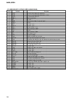
FLDT
O
Serial data signal output to the display driver.
2
FLCK
O
Serial clock signal output to the display driver. L: Active
3
A1-IN
I
A1 Control input. (Fixed at L)
4
SIRCS
I
Remote control input.
5 - 7
NC
—
Not used.
8
BYTE
I
Data bus changed input. (Connected to ground.)
9
CNVSS
—
Ground.
10
XIN-T
I
Not used . (open)
11
XOUT-T
O
Not used . (open)
12
S.RST
I
System rest input. L : ON
13
XOUT
O
Main clock output. (10MHz)
14
GND
—
Ground.
15
XIN
I
Main clock input. (10MHz)
16
VCC
—
Power supply. (+3.3V)
17
NMI
I
Fixed at H. (Pull-up)
18
DQSY
I
Digital in sync input. (Record system)
19
P.DOWN
I
Power down detection input. L: Power down
20
SQSY
I
ADIP (MO) sync or subcode Q (PIT) sync input from CXD2662R.(Playback system)
21
KB.CLK
I
Keyboard clock input. (Fixed at H)
22
KB.DATA
I
Keyboard data input. (Fixed at H)
23
IIC BUSY
I
IIC cable connect check. L: Active
24
A1 OUT
O
Not used. (open)
25
XINIT
I
Interrupt status input from CXD2662R.
26
*BEEP
O
Not used. (open)
27
LRCKI
O
Not used. (open)
28
IIC POWER
O
Media commucator start-up check.
29
IIC CLK
O
IIC serial clock output.
30
IIC DATA
I/O
IIC serial data input/output.
31
SWDT
O
Writing data signal output to the serial bus.
32
SRDT
I
Reading data signal input from the serial bus.
33
SCLK
O
Clock signal output to the serial bus.
34
KB.CLK-CTRL
O
Keyboard clock ON/OFF signal output. L: OFF H: ON
35
CLIP-TX
O
Not used. (open)
36
CLIP-RX
I
Not used. (open)
37
XBCK1
O
Not used. (open)
38
MUTE
O
Line out muting output. L: Mute
39
ADA.RESET
O
Reset signal output to the AK4524. L: Active
Description
Pin Name
Pin No.
I/O
• IC1 M30803MG-107FP SYSTEM CONTROL (MAIN BOARD)
Summary of Contents for MDS-JE470 - Md Player
Page 69: ...69 MDS JE470 ...

