background image

67

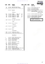
Ref. No.

Part No.

Description

Remarks

Ref. No.

Part No.

Description

Remarks

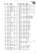
MDS-JE480

MAIN

PT

< VIBRATOR >

X15

1-795-004-21 VIBRATOR, CERAMIC (10MHz)

X550

1-767-406-21 VIBRATOR, CRYSTAL (11.2896MHz)

******************************************************

1-683-584-11 PT BOARD

********

< CAPACITOR >

0

C910

1-113-920-11 CERAMIC

0.0022uF

20%

250V

C923

1-131-992-91 CERAMIC CHIP

100000PF

35V

C924

1-131-992-91 CERAMIC CHIP

100000PF

35V

C951

1-131-992-91 CERAMIC CHIP

100000PF

35V

C952

1-131-992-91 CERAMIC CHIP

100000PF

35V

< CONNECTOR >

*

CN900

1-580-230-11 PIN, CONNECTOR (PC BOARD) 2P

< DIODE >

D910

8-719-988-61 DIODE   1SS355TE-17

< LINE FILTER >

0

LF900

1-419-625-11 COIL, LINE FILTER

< RELAY >

0

RY910

1-755-356-11 RELAY

< TRANSFORMER >

0

TR950

1-437-335-11 TRANSFORMER, POWER (US)

0

TR950

1-437-336-11 TRANSFORMER, POWER (AEP, UK, RU)

******************************************************

MISCELLANEOUS

*************

0

1-770-019-51 ADAPTOR, CONVERSION PLUG (UK)

9

1-792-811-11 WIRE (FLAT TYPE) (23 CORE)

0

12

1-777-071-63 CORD, POWER (AEP, UK, RU)

0

12

1-783-532-32 CORD, POWER (US)

*

14

1-569-972-21 SOCKET, SHORT 2P

55

1-757-929-11 WIRE (FLAT TYPE) (15 CORE)

357

1-678-514-11 PWB, FLEXIBLE

0

358

A-4672-541-A OPTICAL PICK-UP KMS-260E

HR901

1-500-670-22 HEAD, OVER LIGHT

M101

A-4735-757-A MOTOR ASSY, SPINDLE

M102

A-4735-076-A MOTOR ASSY, SLED

M103

A-4735-074-A MOTOR ASSY, LOADING

S102

1-771-957-11 SWITCH, PUSH (2 KEY) (REFLECT/PROTECT SW)

0

TR900

1-435-543-11 TRANSFORMER, POWER (US)

0

TR900

1-435-544-11 TRANSFORMER, POWER (AEP, UK, RU)

******************************************************

ACCESSORIES

***********

1-476-723-11 REMOTE COMMANDER (RM-D10E)
1-776-263-12 CORD, CONNECTION (AUDIO)
1-574-264-11 CORD, LIGHT PLUG (OPTICAL)
4-238-553-12 INSTRUCTION MANUAL (ENGLISH) (EXCEPT RU)
4-238-553-21 INSTRUCTION MANUAL

(FRENCH,DUTCH,SWEDISH,GERMAN,SPANISH,

ITALIAN,POLISH)(AEP)

4-238-553-31 INSTRUCTION MANUAL (DANISH,FINNISH)

(AEP)

4-238-553-41 INSTRUCTION MANUAL (PORTUGUESE)(AEP)
4-238-553-51 INSTRUCTION MANUAL (RUSSIAN)(AEP)
4-238-553-61 INSTRUCTION MANUAL (RUSSIAN)(RU)
4-981-643-11 COVER, BATTERY (For RM-D10E)

The components identified by mark 

0

  or dotted

line with mark 

0

 are critical for safety.

Replace only with part number specified.

Ver. 1.3

www. xiaoyu163. com

QQ 376315150

9

9

2

8

9

4

2

9

8

TEL 13942296513

9

9

2

8

9

4

2

9

8

0

5

1

5

1

3

6

7

3

Q

Q

TEL  13942296513  QQ  376315150  892498299 

TEL  13942296513  QQ  376315150  892498299 

http://www.xiaoyu163.com

http://www.xiaoyu163.com

Summary of Contents for MDS-JE480

Page 1: ...Eight to Fourteen Modulation Number of channels 2 stereo channels Frequency response 5 to 20 000 Hz 0 5 dB during play Signal to noise ratio Over 96 dB during play Wow and flutter Below measurable limit Inputs ANALOG IN Jack type phono Impedance 47 kilohms Rated input 500 mVrms Minimum input 125 mVrms DIGITAL OPTICAL IN Connector type square optical Impedance 660 nm optical wave length Outputs ANA...

Page 2: ...rmance of procedures other than those specified herein may result in hazardous radia tion exposure Notes on chip component replacement Never reuse a disconnected chip component Notice that the minus side of a tantalum capacitor may be damaged by heat Flexible Circuit Board Repairing Keep the temperature of soldering iron around 270 C during repairing Do not touch the soldering iron on the same con...

Page 3: ...through the DIGITAL IN connector the digital connecting cable was unplugged or the digital component turned off Connect the cable or turn the digital component back on E0001 MEMORY NG There is an error in the internal data that the deck needs in order to operate Consult your nearest Sony dealer E010 E0201 LOADING NG 1 LASER NG There is a problem with the optical pickup The optical pick up may have...

Page 4: ...splay changes to er refresh When complete is displayed it means erasure has completed Be sure to check the following after executing this mode Data has been erased Perform recording and playback and check that the mechanism is normal Mode for erasing the total time of recording and playback Procedure 1 Press the lAMSL knob when displayed as tm refresh 2 Press the YES button when the display change...

Page 5: ... 3 1 Disassembly flow 13 3 2 Upper Case 408226 14 3 3 Front Panel Section 14 3 4 Main Board 15 3 5 PT Board 15 3 6 Mechanism Deck Section MDM 7S1A 16 3 7 Over Light Head HR901 BD Board 16 3 8 Holder Assy 17 3 9 Loading Motor Assy M103 17 3 10 Sled Motor Assy M102 Slider 18 3 11 Optical Pick up 18 3 12 Spindle Motor Assy M101 19 4 TEST MODE 20 5 ELECTRICAL ADJUSTMENTS 25 6 DIAGRAMS 6 1 Circuit Boar...

Page 6: ...the deterioration of the optical pick up laser TE TRK error signal Traverse adjustment VC Reference level for checking the signal RF RF signal Check jitter FE Focus error signal I 3V Iop GND TE FE VC RF I 3V Iop GND TE FE VC RF 1 7 for MDM 7S1A I 3V CN105 Iop TE VC GND FE RF SECTION 1 SERVICE NOTES www xiaoyu163 com QQ376315150 9 9 2 8 9 4 2 9 8 TEL 13942296513 9 9 2 8 9 4 2 9 8 0 5 1 5 1 3 6 7 3 ...

Page 7: ...S L knob To select the digit Press the l AMS L knob 6 When the YES button is pressed the display becomes Measu is an arbitrary number 7 As the adjustment results are recorded for the 6 value Leave it as it is and press the YES button 8 Complete will be displayed momentarily The value will be recorded in the non volatile memory and the display will become Iop Write 9 Press the REPEAT button to comp...

Page 8: ...the hole on SL base APC variable resistor Small volume 2 type Big variable resistor 3 type and chip resistor Fig A Small variable resistor 2 type and chip resistor Fig B Fig B type is for repair Abbreviation 260B KMS 260B model 260E KMS 260E model KSN 260B KSN 260E Fig A Fig B CHIP 3 type variable resistor 2 type variable resistor CHIP Hold on SL base Hold on SL base FPC retainer plate FPC retaine...

Page 9: ...s not serve as the specified value for adjustments When performing adjustments use the specified values for adjustments FORCED RESET The system microprocessor can be reset in the following procedure Use these procedure when the unit cannot be operated normally due to the overrunning of the microprocessor etc Procedure Remove the short pin attached to CN406 and then attach it again MAIN BOARD Compo...

Page 10: ...played 8 Press the z REC button to start recording Then press the X button and start recording 9 To check the track mode press the H button to start play 10 To exit the test mode press the 1 button and turn OFF the power When TOC disappears disconnect the power plug from the outlet If the test mode cannot be exited refer to Forced Reset on page 9 Address Physical address on disc Hexadecimal Bit Bi...

Page 11: ... Higher bit 0 1000 t All 0 Lower bit 7 0111 t b0 b1 b2 In this case as b0 b1 and b2 are 1 and others are 0 it can be determined that the retry cause is combined of emphasis ON stereo original copyright exists and write prohibited Hexadecimal t Binary Conversion Table Hexadecimal Binary Hexadecimal Binary 0 1 2 3 4 5 6 7 8 9 A B C D E F 0000 0001 0010 0011 0100 0101 0110 0111 1000 1001 1010 1011 11...

Page 12: ...ted from instruction manual www xiaoyu163 com QQ376315150 9 9 2 8 9 4 2 9 8 TEL 13942296513 9 9 2 8 9 4 2 9 8 0 5 1 5 1 3 6 7 3 Q Q TEL 13942296513 QQ 376315150 892498299 TEL 13942296513 QQ 376315150 892498299 http www xiaoyu163 com http www xiaoyu163 com ...
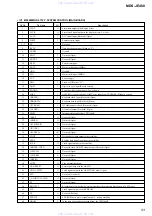
Page 13: ... 3 8 HOLDER ASSY 3 9 LOADING MOTOR ASSY M103 3 10 SLED MOTOR ASSY M102 3 12 SPINDLE MOTOR ASSY M101 3 7 BD BOARD 3 8 HOLDER ASSY Note 1 The processes enclosed with remove in the any order Note 2 You cannot go to the next process until every process enclosed with has done www xiaoyu163 com QQ376315150 9 9 2 8 9 4 2 9 8 TEL 13942296513 9 9 2 8 9 4 2 9 8 0 5 1 5 1 3 6 7 3 Q Q TEL 13942296513 QQ 37631...

Page 14: ...o screws BVTP3x8 3 Two screws BVTP3x8 7 Front panel 4 Claw 4 Claw 1 Wire flat type CN3 2 Lead with connector 5 5 6 www xiaoyu163 com QQ376315150 9 9 2 8 9 4 2 9 8 TEL 13942296513 9 9 2 8 9 4 2 9 8 0 5 1 5 1 3 6 7 3 Q Q TEL 13942296513 QQ 376315150 892498299 TEL 13942296513 QQ 376315150 892498299 http www xiaoyu163 com http www xiaoyu163 com ...
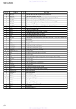
Page 15: ...t type CN2 3 Wire flat type CN3 8 MAIN board 3 Three screws PTTWH M3 1 Connector CN900 4 PT board 2 Nylon rivet dia 3 www xiaoyu163 com QQ376315150 9 9 2 8 9 4 2 9 8 TEL 13942296513 9 9 2 8 9 4 2 9 8 0 5 1 5 1 3 6 7 3 Q Q TEL 13942296513 QQ 376315150 892498299 TEL 13942296513 QQ 376315150 892498299 http www xiaoyu163 com http www xiaoyu163 com ...
Page 16: ...6 8 FLEXIBLE board CN101 9 BD board 1 Connector CN104 2 Screw P1 7X6 Note 1 If you disconnect the connector CN104 you can remove the BD board without removing the over write head HR901 Note 2 Be careful to handle the over write head HR901 because it is easy to be damaged www xiaoyu163 com QQ376315150 9 9 2 8 9 4 2 9 8 TEL 13942296513 9 9 2 8 9 4 2 9 8 0 5 1 5 1 3 6 7 3 Q Q TEL 13942296513 QQ 37631...

Page 17: ... spring holder 2 Two screws PWH1 7x2 5 4 Loading motor Assy M103 1 Belt loading 3 www xiaoyu163 com QQ376315150 9 9 2 8 9 4 2 9 8 TEL 13942296513 9 9 2 8 9 4 2 9 8 0 5 1 5 1 3 6 7 3 Q Q TEL 13942296513 QQ 376315150 892498299 TEL 13942296513 QQ 376315150 892498299 http www xiaoyu163 com http www xiaoyu163 com ...
Page 18: ...ical pick up KMS 260B 260E 7 Main shaft 6 Two screws K2X6 4 Screw BTP2X6 5 Base BU A 3 Gear SD 2 Screw M1 7 tapping 0 SL base 9 Screw P1 7X6 8 3 10 SLED MOTOR ASSY M102 SLIDER 3 11 OPTICAL PICK UP www xiaoyu163 com QQ376315150 9 9 2 8 9 4 2 9 8 TEL 13942296513 9 9 2 8 9 4 2 9 8 0 5 1 5 1 3 6 7 3 Q Q TEL 13942296513 QQ 376315150 892498299 TEL 13942296513 QQ 376315150 892498299 http www xiaoyu163 co...
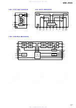
Page 19: ...ping 2 3 12 SPINDLE MOTOR ASSY M101 www xiaoyu163 com QQ376315150 9 9 2 8 9 4 2 9 8 TEL 13942296513 9 9 2 8 9 4 2 9 8 0 5 1 5 1 3 6 7 3 Q Q TEL 13942296513 QQ 376315150 892498299 TEL 13942296513 QQ 376315150 892498299 http www xiaoyu163 com http www xiaoyu163 com ...
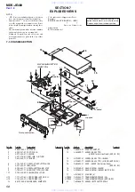
Page 20: ...of entering the test mode Procedure 1 While pressing the lAMS L knob and x button connect the power plug to an outlet and release the lAMS L knob and x button When the test mode is set Check will be displayed Rotating the l AMS L knob switches between the following three groups y Check y Service y Develop y Procedure 2 While pressing the l AMS L knob connect the power plug to the outlet and releas...

Page 21: ...odes as shown below The groups can be switched by rotating the l AMS L knob After selecting the group to be used press the YES button After setting a certain group rotating the l AMS L knob switches between these modes Refer to Group in the table for details selected All adjustments and checks during servicing can be performed in the test mode in the Service group For details of each adjustment mo...

Page 22: ...cording mode 1 Set a recordable disc in the unit 2 Rotate the l AMS L knob and display CREC1 MODE C35 3 Press the YES button to change the display to CREC1 MID 4 When access completes the display changes to CREC 1 and REC lights up Note The numbers displayed shows you the recording position addresses 2 Changing the parts to be recorded 1 When the YES button is pressed during continuous recording t...

Page 23: ...display as the initial mode 1 Mode display Displays TEMP ADJUST CPLAY1MODE etc 2 Error rate display Displays the error rate in the following way C AD C Indicates the C error AD Indicates ADER 3 Address display The address is displayed as follows MO recordable disc CD playback only disc If the REC MODE button is pressed the display switches from groove to pit or vice versa h s MO pit and CD h a MO ...

Page 24: ...d from 07 CHECK 6 After completing to test item 12 check OK or NG will be displayed If all items are OK CHECKALL OK will be displayed If any item is NG it will be displayed as NG xxxx When CHECK ALL OK is displayed it means that the optical pick up is normal Check the operations of the other spindle motor thread motor etc When displayed as NG xxxx it means that the optical pick up is faulty In thi...

Page 25: ...ck the threading mechanism etc Start NG NG NG OK OK OK Laser Power Check 5 6 2 See page 28 5 6 3 See page 28 5 6 4 See page 29 Iop Compare Auto Check Replace Optical pick up or MDM 7S1A Note 260B KMS 260B 260E KMS 260E www xiaoyu163 com QQ376315150 9 9 2 8 9 4 2 9 8 TEL 13942296513 9 9 2 8 9 4 2 9 8 0 5 1 5 1 3 6 7 3 Q Q TEL 13942296513 QQ 376315150 892498299 TEL 13942296513 QQ 376315150 892498299...

Page 26: ...AYED See page 24 Abbreviation OP Optical pick up 5 7 INITIAL SETTING OF ADJUSTMENT VALUE See page 31 5 9 TEMPERATURE COMPENSATION OFFSET ADJUSTMENT See page 31 5 10 LASER POWER ADJUSTMENT See page 31 5 12 TRAVERSE ADJUSTMENT See page 32 5 13 FOCUS BIAS ADJUSTMENT See page 33 5 16 AUTO GAIN CONTROL OUTPUT LEVEL ADJUSTMENT See page 34 OP change in Err Display mode Iop write Spdl change in Err Displa...

Page 27: ...fter completing the adjustments exit the test mode Perform the adjustments and checks in group S of the test mode 3 Perform the adjustments to be needed in the order shown 4 Use the following tools and measuring devices Check Disc MD TDYS 1 Parts No 4 963 646 01 Test Disk MDW 74 GA 1 Parts No 4 229 747 01 Laser power meter LPM 8001 Parts No J 2501 046 A or MD Laser power meter 8010S Parts No J 250...

Page 28: ...up label For details of the method for checking this value refer to 5 8 Recording and Displaying Iop Information R 5 6 3 Iop Compare The current Iop value at laser power 7 mw output and reference Iop value set at shipment written in the nonvolatile memory are compared and the rate of increase decrease will be displayed in percentage Note Perform this function with the optical pick up set at room t...

Page 29: ... Procedure 1 Press the YES button If LDPWR is displayed it means that the laser power check has not been performed In this case perform the laser power check and Iop compare and then repeat from step 1 2 If a disc is in the mechanical deck it will be ejected forcibly DISC IN will be displayed in this case Load a test disc MDW 74 GA 1 which can be recorded 3 If a disk is loaded at step 2 the check ...

Page 30: ...the focus bias and check the focus tolerance amount Checking Procedure 1 Load a continuously recorded test disc MDW 74 GA 1 Refer to 5 5 Using the Continuously Recorded Disc 2 Rotate the l AMS L knob and display CPLAY1 MODE 3 Press the YES button and display CPLAY1 MID 4 The display change to C AD 5 Press the MENU NO button and display CPLAY1 MODE 6 Rotate the lAMS L knob and display FBIAS CHECK 7...

Page 31: ...FFSET ADJUSTMENT Save the temperature data at that time in the non volatile memory as 25 C reference data Note 1 Usually do not perform this adjustment 2 Perform this adjustment in an ambient temperature of 22 C to 28 C Perform it immediately after the power is turned on when the internal temperature of the unit is the same as the ambient temperature of 22 C to 28 C 3 When D101 has been replaced p...

Page 32: ...aveform varies at intervals of approx 2 Adjust the wave form so that the specified value is satisfied as much as possible Read power traverse adjustment Traverse Waveform 7 Press the YES button and save the result of adjustment to the non volatile memory EFB SAVE will be displayed for a moment Then EFB MO W will be displayed 8 Rotate the l AMS L knob so that the waveform of the oscilloscope become...

Page 33: ...ob and display CPLAY1 MODE 3 Press the YES button and display CPLAY1 MID 4 The display change to C AD 5 Press the MENU NO button and display CPLAY1 MODE 6 Rotate the l AMS L knob and display FBIAS AD JUST 7 Press the YES button and display a The first four digits indicate the C error rate the two digits after indicate ADER and the 2 digits after a indicate the focus bias value 8 Rotate the lAMS L ...

Page 34: ... Press the YES button and display a Check that the C error is below 100 and ADER is below 2 10 Press the MENU NO button next press the A EJECT button and remove the continuously recorded disc Note 1 If the C error and ADER are above other than the speci fied value at points a step 9 in the above or b step 8 in the above the focus bias adjustment may not have been carried out properly Adjust perfor...

Page 35: ...IDE A D101 CN101 1 21 CN103 CN102 CN105 IC701 IC201 IC101 IC195 IC933 1 4 1 5 8 1 1 7 27 23 1 3 1 30 90 61 1 3 5 4 24 13 37 48 31 60 1 12 36 25 120 91 www xiaoyu163 com QQ376315150 9 9 2 8 9 4 2 9 8 TEL 13942296513 9 9 2 8 9 4 2 9 8 0 5 1 5 1 3 6 7 3 Q Q TEL 13942296513 QQ 376315150 892498299 TEL 13942296513 QQ 376315150 892498299 http www xiaoyu163 com http www xiaoyu163 com ...
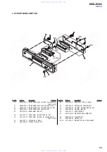
Page 36: ...d DISPLAY board BD board MAIN board PT board www xiaoyu163 com QQ376315150 9 9 2 8 9 4 2 9 8 TEL 13942296513 9 9 2 8 9 4 2 9 8 0 5 1 5 1 3 6 7 3 Q Q TEL 13942296513 QQ 376315150 892498299 TEL 13942296513 QQ 376315150 892498299 http www xiaoyu163 com http www xiaoyu163 com ...
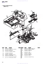
Page 37: ...ge variations may be noted due to normal produc tion tolerances Circled numbers refer to waveforms Signal path E PB j REC l REC DIGITAL IN Caution Pattern face side Parts on the pattern face side seen from the Side B pattern face are indicated Parts face side Parts on the parts face side seen from the Side A parts face are indicated C B These are omitted E Q B These are omitted C E B These are omi...

Page 38: ...ADDT DADT BCK LRCK REFLECT PROTECT LD LO SDA SCL EEP WP UNREG 12V 65 LIMIT IN OUT SW S101 LIMIT IN PLAY SW SIGNAL PATH PLAY ANALOG OUT REC ANALOG IN REC DIGITAL IN S103 OUT SW S104 PLAY SW REC SW S105 REC POSITION XBCKI LRCKI S102 REFLECT PROTECT DETECT HIGH REFELECT RATE WRITE PROTECT LOW REFELECT RATE UN PROTECT OVER WRITE HEAD DRIVE IC181 Q181 182 WAVE SHAPER IC600 1 2 OPTICAL RECEIVER IC611 11...

Page 39: ...ENTER S713 S701 706 711 712 S714 716 721 724 S726 A B PD DEMO SIRCS OSCI C769 R769 OSCO LINE AMP IC360 OSC IC550 C Page38 Page38 Page38 SIGNAL PATH RST XIN XOUT X15 10MHz SYSTEM CONTROLLER IC1 2 2 S RST 8 9 12 10 13 6 2 1 VCOM LOUT 15 14 ROUT 16 11 39 72 15 13 61 62 60 52 1 LED DRIVE Q755 D775 MD LP 2 58 59 63 38 STB 81 4 4 5 88 87 1 3 1 2 84 19 12 32V REGULATOR Q427 32V FL DRIVER IC760 B 3 3V REG...

Page 40: ...L401 C405 C998 R303 R302 C301 C904 C220 C219 C205 C241 R217 R211 R210 R214 R120 R207 R202 R203 C215 TP504 TP219 TP612 C703 5 1 3 4 IC201 C117 R707 R113 R122 R107 R116 R119 R117 IC101 R110 R114 C122 R121 R708 R208 C115 R212 C113 C107 C120 CN103 C110 C119 C118 R112 R115 C121 C406 C299 TP501 TP615 TP503 C899 C221 R106 R711 R706 R111 C108 C302 L550 BG1 R101 R102 R108 R118 L899 R201 R209 C902 R301 IC40...

Page 41: ...7 F B 0 001 F B UN5113 TX F B CXA2523AR 1 6 LD ON GND VCC WRPWR IOP MOD 2 2 M 5V MGND PSB RF DTRF CKRF XLRF F E D C B A J I 6 7 5 9 8 2 4 3 10 11 12 13 14 15 16 SPRD SPFD FRDR FFDR TFDR TRDR SRDR SFDR 16 15 I B A F C D E J 13 14 A B C D E F PD TEMPI GND SWDT SCLK XLAT VCC TE CSLED SE ADFM ADIN ADAGC ADFG AUX FE ABCD BOTM PEAK RFAGC RF RFO MORFI MORFO E B I VCC C J D F VC TEMPR TRK TRK FCS FCS A PD...

Page 42: ...Y XINT SENS A00 A01 A02 A03 A04 A05 A06 A07 A08 A09 XWE XOE D0 D1 D2 D3 A00 A01 A02 A03 A04 A05 A06 A07 A08 A09 XRAS XCAS TRDR TFDR FFDR FRDR SRDR SFDR SPRD SPFD XBCK LRCK DADT ADDT SWDT SCLK XLAT SRDT SENS DOUT DIN0 DIN1 D1 D2 D0 D3 5 8 9 2 3 4 6 7 10 11 12 MGND SDA SCL GND ADDT M 5V BCK GND H 5V DADT MGND LRCK 5V DOUT HGND A2 A1 A0 DADTI LRCKI GND XBCKI DIN0 DIN1 MCKGND MCLK SRDT XLATCH SWDT SCL...

Page 43: ...CL EEP WP XBUSY OUT SW XLATCH PROTECT REFRECT SDA SCL EEP WP SHOCK XBUSY SWDT SWDT SRDT SRDT OUT SW SCLK SCLK XLATCH PLAY SW SENS DIG RST REC SW WRPWR LIMIT IN LDON MOD DQSY SQSY XINT SQSY DQSY XINT JOG 1 JOG 0 FLCS FLCK FLDT FLCS JOG 1 JOG 0 KEY 1 KEY 2 RMC KEY 0 RMC FLCK FLDT KEY 0 KEY 1 KEY 2 DADT LRCK ADDT BCLK LRCK DADT ADDT ADA RESET EMF BCLK ADA RESET EMF PLAY SW DIG RST REC SW WRPWR LIMIT ...

Page 44: ...A2 11ES2 NTA2 11ES2 NTA2 11ES2 NTA2 11ES2 NTA2 11ES2 NTA2 470 16V 470 16V 10000 16V 47k 0 33 50V 11EQS04 TB 11EQS04 TB 1k 10P 4 7k 10 50V 2SB1375 UN4211 TA 100 16V 33 25V RD4 7ES T2B2 M5F7805L 0 1 0 1 10000 16V M62016L 2SD2144S TP UVW 0 01 0 1 JW MTZJ T 72 33D BATTERY 0 1 470 10V 100k 2 2k JW JW 10k 0 1 0 1 LB1641 LD IN LD OUT LOAD IN LOAD OUT LD LOW S RST STB 32V AC1 AC2 3 3V GND 5V BACK 3 3V SYS...

Page 45: ...281 Q181 C276 C176 C160 C270 Q421 E C424 C425 C423 D421 D401 D403 D402 D467 D466 D462 D461 D411 D412 D408 1 2 D409 C491 IC490 JW004 JW005 JW008 JW010 JW011 JW019 JW020 JW026 JW030 JW042 JW044 JW045 JW048 JW049 JW050 JW051 JW052 JW053 JW064 JW065 JW066 JW067 JW068 JW069 JW070 JW071 JW072 JW073 JW074 JW075 JW076 JW077 JW092 JW093 JW095 JW096 JW097 JW098 JW100 JW101 JW112 JW115 JW116 JW127 JW128 JW12...

Page 46: ...ECT D775 MD LP C765 C781 Q767 FL750 FL TUBE AMS M x X M z h Z R725 R724 R723 C740 R726 R1726 R722 JW752 JW751 S746 JW750 CN720 4 1 JW733 JW734 JW1726 JW1733 Q726 E S722 PLAY MODE S723 REPEAT S724 LEVEL DISPLAY CHAR S726 D726 STANDBY JW735 JW736 11 11 1 683 587 KEY SW BOARD S714 CLEAR 2 3 4 5 6 7 8 9 10 11 12 A 1 B C D E F G 6 9 PRINTED WIRING BOARD DISPLAY SECTION See page 36 for Circuit Board Loc...

Page 47: ... G4 G5 G6 G7 G8 G9 G10 G11 G12 G13 S25 S1 S3 S5 S7 S9 S11 S12 S13 S15 S17 S19 S21 S2 S4 S6 S8 S10 S14 S16 S18 S20 S22 S24 S23 S27 S28 S26 S35 S34 S33 S32 S31 S30 S29 G1 G2 G3 G4 S28 S27 S26 S25 S24 S23 S22 S21 S20 S19 S18 S17 S16 S15 S14 S13 S12 S11 S10 S9 S8 S7 S6 S5 S4 S3 S2 S1 G5 G6 G7 G8 G9 G10 G11 G12 G13 YES MENU NO CLEAR KEY2 GND POWER LED 3 3V INPUT REC MODE KEY2 JOG1 KEY1 JOG0 KEY0 FLDT F...

Page 48: ...900 2 3 4 A 1 B C D E F G H EP900 LF900 TR900 RY910 C910 CN900 D910 JW901 JW904 C924 C923 CN921 EARTH PLATE LINE FILTER RELAY 0 0022 250V 2P 1SS133T 72 C951 0 1 C952 TR950 0 1 0 1 0 1 WIRE 10P AC IN NOT REPLACEABLE BUILT IN TRANSFORMER CHASSIS Ver 1 1 2003 04 w w w x i a o y u 1 6 3 c o m Q Q 3 7 6 3 1 5 1 5 0 9 9 2 8 9 4 2 9 8 T E L 1 3 9 4 2 2 9 6 5 1 3 9 9 2 8 9 4 2 9 8 0 5 1 5 1 3 6 7 3 Q Q TE...

Page 49: ...64R External capacitor connection pin for the sled error signal LPF Sled error signal output to the CXD2664R FM signal output of ADIP ADIP signal comparator input ADFM is connected with AC coupling External capacitor connection pin for AGC of ADIP ADIP duplex signal output to the CXD2664R I3 signal temperature signal output to the CXD2664R Focus error signal output to the CXD2664R Light amount sig...

Page 50: ...m clock input Input terminal during OSCN H Internal oscillating circuit control signal input Ground System clock frequency setting Digital audio input Optical input Digital audio input Optical input Not used Digital audio output Optical output Not used Serial data input LR clock input Serial data bit clock input Power supply Ground Data input from the A D converter Data output to the D A converter...

Page 51: ...input for the recording playback EFM master PLL Light amount signal peak hold input Light amount signal bottom hold input Light amount signal input Focus error signal input from the CXA2523AR Auxiliary A D input Middle point voltage input from the CXA2523AR Monitor output of the A D converter input signal Not used Open A D converter operational range upper limit voltage input Fixed at H A D conver...

Page 52: ...WM output for the laser digital APC Not used Open Tracking servo drive PWM output Tracking servo drive PWM output Focus servo drive PWM output Focus servo drive PWM output 4Fs clock signal output Not used Open Sled servo drive PWM output Sled servo drive PWM output Spindle servo drive PWM output Spindle servo drive PWM output Spindle CAV servo FG signal input Test input Fixed at L EFM output when ...

Page 53: ...LK O Not used Open 30 IIC DATA I O Not used Open 31 SWDT O Writing data signal output to the serial bus 32 SRDT I Reading data signal input from the serial bus 33 SCLK O Clock signal output to the serial bus 34 KB CLK CTRL O Keyboard clock ON OFF signal output Not used Open 35 CLIP TX O Not used Open 36 CLIP RX I Not used Open 37 XBCK1 O Not used Open 38 MUTE O Line out muting output 39 ADA RESET ...

Page 54: ...Ground 65 LOAD LO O Loading motor voltage control output 66 LOAD OUT O Loading motor control output H eject 67 LOAD IN O Loading motor control output H loading 68 71 MODEL SEL 0 3 O Not used Open 72 EMF O Deemphasis control signal output to the AK4552 73 80 NC O Not used Open 81 STB O Strobe signal output to the power supply circuit H Power supply ON L standby 82 BEEP SW O Not used Open 83 REC O N...

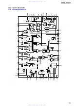
Page 55: ...I 13 GND 12 APCREF 11 APC 10 PD 9 F 8 E 7 D 6 C 5 B 4 A 3 VC VI CONV BGR VREF SCRI PARA DECODE AUXSW COMMAND IVR GSW FF FBAL FF TG SEA 1 2 TG TEA WBL 3T EQ DET ADIP AGC WBL BPF22 BPFC ABCDA FEA WBL ATA CVB RFA1 1 2 1 2 GRVA OFST RFA2 GRV HLPT PTGR 2 1 1 2 BOTTOM PEAK RF AGC EQ EQ DET P P WBL 3T WBL TEMP PBH USROP USRC 3T BPF3T PEAK3T 1 I 2 J RFA3 PBSW AUX SW IV ESW EBAL www xiaoyu163 com QQ3763151...

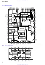
Page 56: ...12 XRST 11 SENS 10 SRDT 9 VSC0 8 XLAT 7 SCLK 6 SWDT 4 MNT3 SLOC 5 VDC0 3 MNT2 XBUSY 2 MNT1 SHCK 1 MNT0 FOK PWM GENERATOR AUTO SEQUENCER SERVO DSP CPU I F MONITOR CONTROL SPINDLE SERVO EACH BLOCK EACH BLOCK DIGITAL AUDIO I F SAMPLING RATE CONVERTER CLOCK GENERATOR SUBCODE PROCESSOR EACH BLOCK A D CONVERTER ANALOG MUX EFM ACIRC ENCODER DECODER PLL SHOCK RESISTANT MEMORY CONTROLLER ATRAC ATRAC3 ENCOD...

Page 57: ...1 2 4 5 6 7 8 16 15 14 13 12 11 10 ROUT LOUT VCOM POWER DOWN RESET BICK MCLK LRCK SDTI RIN LIN 3 VSS VA AVCC DVCC VD DEM0 DEM1 SDTO MODULATOR MODULATOR DEEMPHASIS CONTROL SERIAL I O INTERFACE COMMON VOLTAGE MODULATOR MODULATOR CLOCK DRIVER DECIMATION FILTER DECIMATION FILTER 8X INTERPOLATOR 8X INTERPOLATOR LPF LPF 9 PD www xiaoyu163 com QQ376315150 9 9 2 8 9 4 2 9 8 TEL 13942296513 9 9 2 8 9 4 2 9...

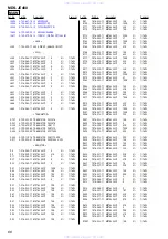
Page 58: ...rt No Description Remarks Ver 1 4 1 X 4953 448 1 FOOT ASSY 2 4 232 237 01 FOOT DIA 30 3 4 977 358 01 CUSHION 4 3 531 576 41 RIVET DIA 3 NYLON 5 1 683 584 11 PT BOARD 6 3 703 249 01 SCREW S TIGHT PTTWH 3X6 7 4 231 555 01 INSULATOR 8 4 228 643 11 SCREW BVTTWH M3 STEP 9 1 792 811 11 WIRE FLAT TYPE 23 CORE 11 3 703 244 00 BUSHING 2104 CORD 012 1 777 071 63 CORD POWER AEP UK RU 012 1 783 532 32 CORD PO...

Page 59: ...2 4 231 928 31 KNOB AMS SILVER for Hair line Finish AEP UK RU 53 3 354 981 11 SPRING SUS RING 54 4 951 620 01 SCREW 2 6X8 BVTP 55 1 757 929 11 WIRE FLAT TYPE 15 CORE 56 4 228 630 01 SPRING LID TENSION COIL 57 4 228 629 21 LID MD SILVER AEP UK RU 57 4 228 629 81 LID MD BLACK 58 1 683 587 11 KEY SW BOARD 59 A 4727 955 A DISPLAY BOARD COMPLETE 60 4 949 935 41 CUSHION FL 61 4 212 590 22 HOLDER FL FL75...

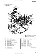
Page 60: ...ING SHT ASSY LEAF 309 A 468 063 8A LOCK HOLDER 310 4 229 533 02 SPRING STOPPER TORSION 311 4 231 118 01 SPRING HOLDER TENSION 312 A 4680 638 B RETAINER COMPLETE ASSY 313 4 227 013 01 SPRING EJ TENSION 314 4 226 996 01 LIMITTER EJ 315 4 226 995 01 SLIDER EJ 316 4 226 997 04 SLIDER 317 4 226 998 01 LEVER CHG 318 4 227 006 01 GEAR SA 319 A 4735 075 B HOLDER ASSY 320 4 226 994 01 GUIDE L 2 7 685 850 0...

Page 61: ...SIS 362 4 232 270 01 SCREW 1 7X3 5 PWH 363 4 226 990 04 BASE BU A The components identified by mark 0 or dotted line with mark 0 are critical for safety Replace only with part number specified 364 4 230 716 01 SPRING SPDL TORSION 365 4 227 004 01 GEAR LC 366 4 227 005 01 GEAR LD 367 4 227 009 01 GEAR SD 368 4 227 008 01 GEAR SC HR901 1 500 670 22 HEAD OVER LIGHT M101 A 4735 757 A MOTOR ASSY SPINDL...

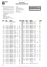
Page 62: ...77 11 CERAMIC CHIP 0 033uF 10 16V C216 1 125 889 91 CERAMIC CHIP 2 2uF 10 10V C219 1 162 927 11 CERAMIC CHIP 100PF 5 50V C220 1 125 891 11 CERAMIC CHIP 0 47uF 10 10V C221 1 162 970 11 CERAMIC CHIP 0 01uF 10 25V C230 1 164 156 11 CERAMIC CHIP 0 1uF 25V C231 1 164 156 11 CERAMIC CHIP 0 1uF 25V C233 1 164 156 11 CERAMIC CHIP 0 1uF 25V C234 1 164 156 11 CERAMIC CHIP 0 1uF 25V C235 1 164 156 11 CERAMIC...

Page 63: ... 5 1 16W R117 1 216 845 11 METAL CHIP 100K 5 1 16W R118 1 216 825 11 METAL CHIP 2 2K 5 1 16W R119 1 216 837 11 METAL CHIP 22K 5 1 16W R120 1 216 839 11 METAL CHIP 33K 5 1 16W R121 1 216 825 11 METAL CHIP 2 2K 5 1 16W R122 1 216 833 11 METAL CHIP 10K 5 1 16W R201 1 216 815 11 METAL CHIP 330 5 1 16W R202 1 216 819 11 METAL CHIP 680 5 1 16W R203 1 216 809 11 METAL CHIP 100 5 1 16W R205 1 216 833 11 M...

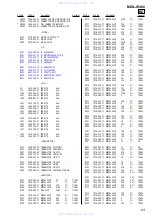
Page 64: ...216 833 11 METAL CHIP 10K 5 1 16W R760 1 216 809 11 METAL CHIP 100 5 1 16W R761 1 216 809 11 METAL CHIP 100 5 1 16W R762 1 216 809 11 METAL CHIP 100 5 1 16W R763 1 216 809 11 METAL CHIP 100 5 1 16W R767 1 216 845 11 METAL CHIP 100K 5 1 16W R769 1 216 827 11 METAL CHIP 3 3K 5 1 16W R775 1 216 813 11 METAL CHIP 220 5 1 16W R781 1 216 805 11 METAL CHIP 47 5 1 16W R782 1 216 809 11 METAL CHIP 100 5 1 ...

Page 65: ... 933 11 ELECT 100uF 20 16V C505 1 107 826 11 CERAMIC CHIP 0 1uF 10 16V C509 1 216 864 11 METAL CHIP 0 5 1 16W C519 1 162 964 11 CERAMIC CHIP 0 001uF 10 50V C523 1 126 933 11 ELECT 100uF 20 16V C524 1 107 826 11 CERAMIC CHIP 0 1uF 10 16V C530 1 107 826 11 CERAMIC CHIP 0 1uF 10 16V C550 1 107 826 11 CERAMIC CHIP 0 1uF 10 16V C551 1 126 933 11 ELECT 100uF 20 16V C552 1 107 826 11 CERAMIC CHIP 0 1uF 1...

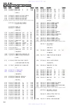
Page 66: ...R115 1 216 805 11 METAL CHIP 47 5 1 16W R163 1 216 845 11 METAL CHIP 100K 5 1 16W R164 1 216 809 11 METAL CHIP 100 5 1 16W R165 1 216 829 11 METAL CHIP 4 7K 5 1 16W R166 1 216 833 11 METAL CHIP 10K 5 1 16W R171 1 216 819 11 METAL CHIP 680 5 1 16W R177 1 216 845 11 METAL CHIP 100K 5 1 16W R178 1 216 815 11 METAL CHIP 330 5 1 16W R181 1 216 829 11 METAL CHIP 4 7K 5 1 16W R211 1 216 839 11 METAL CHIP...

Page 67: ...BLE 0358 A 4672 541 A OPTICAL PICK UP KMS 260E HR901 1 500 670 22 HEAD OVER LIGHT M101 A 4735 757 A MOTOR ASSY SPINDLE M102 A 4735 076 A MOTOR ASSY SLED M103 A 4735 074 A MOTOR ASSY LOADING S102 1 771 957 11 SWITCH PUSH 2 KEY REFLECT PROTECT SW 0TR900 1 435 543 11 TRANSFORMER POWER US 0TR900 1 435 544 11 TRANSFORMER POWER AEP UK RU ACCESSORIES 1 476 723 11 REMOTE COMMANDER RM D10E 1 776 263 12 COR...

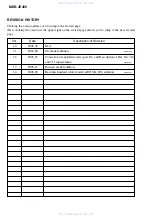
Page 68: ...l addition ENG 03002 1 2 2005 03 Correction of exploded views part No and Description of Ref No 314 and 315 replacement SPM 05011 1 3 2005 11 Russian model addition 1 4 2006 02 Hair line finished silver model AEP UK RU addition SPM 06013 www xiaoyu163 com QQ376315150 9 9 2 8 9 4 2 9 8 TEL 13942296513 9 9 2 8 9 4 2 9 8 0 5 1 5 1 3 6 7 3 Q Q TEL 13942296513 QQ 376315150 892498299 TEL 13942296513 QQ ...
Reviews: