background image

SERVICE MANUAL

Ver 1.0  2001.06

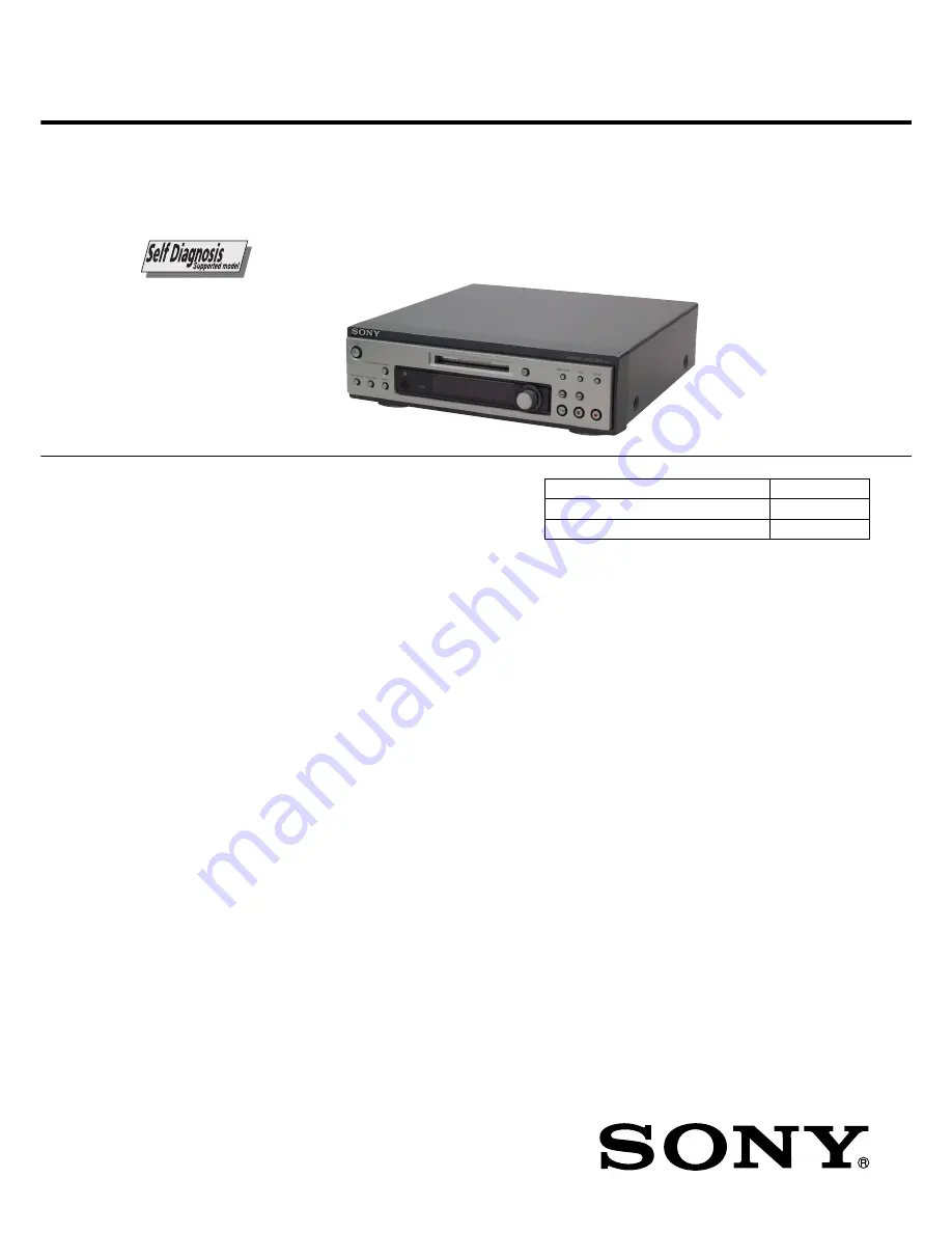
MINIDISC DECK

AEP Model

UK Model

SPECIFICATIONS

MDS-S9

Model Name Using Similar Mechanism

MDS-S50

MD Mechanism Type

MDM-7A

Optical Pick-up Name

KMS-260B

System

MiniDisc digital audio 
system

Disc

MiniDisc

Laser

Semiconductor laser (

λ

 = 

780 nm) Emission 
duration:  continuous

Laser output

MAX 44.6 

µ

W

1)

1)

This output is the value measured at a distance of 
200 mm from the objective lens surface on the 
Optical Pick-up Block with 7 mm aperture.

Laser diode

Material: GaAlAs

Revolutions (CLV)

400 rpm to 900 rpm 

Error correction

ACIRC (Advanced Cross 
Interleave Reed Solomon 
Code)

Sampling frequency

44.1 kHz

Coding

ATRAC (Adaptive 
TRansform Acoustic 
Coding)/ATRAC 3

Modulation system

EFM (Eight-to-Fourteen 
Modulation)

Number of channels

2 stereo channels

Frequency response

5 to 20,000 Hz 

±

0.3 dB

Signal-to-noise ratio

Over 96 dB during play

Wow and flutter

Below measurable limit

Inputs

ANALOG IN

Jack type:  phono
Impedance:  47 kilohms
Rated input:  500 mVrms 
Minimum input:  
125 mVrms

DIGITAL IN

Connector type:  square 
optical
Impedance:  660 nm 
(optical wave length)

Outputs

ANALOG OUT

Jack type:  phono
Rated output:  2 Vrms (at 
50 kilohms)
Load impedance:  over 10 
kilohms

General

Power requirements

230 V AC, 50/60Hz

Power consumption

15 W
0.5 W (at the STANDBY
mode)

Dimensions (approx.)

280 

×

 83 

×

 290 mm (w/

h/d) incl. projecting parts 
and controls

Mass (approx.)

2.4 kg

Supplied accessories

Audio connecting cords (2)
Optical cable (1)
Remote commander (remote) (1)
R6 (size-AA) batteries (2)

Design and specifications are subject to change 
without notice.

US and foreign patents licensed from Dolby 
Laboratories.

9-873-914-11

Sony Corporation

2001F0500-1

Home Audio Company

C

 2001.6

Shinagawa Tec Service Manual Production Group

Summary of Contents for MDS-S9

Page 1: ...2 stereo channels Frequency response 5 to 20 000 Hz 0 3 dB Signal to noise ratio Over 96 dB during play Wow and flutter Below measurable limit Inputs ANALOG IN Jack type phono Impedance 47 kilohms Rated input 500 mVrms Minimum input 125 mVrms DIGITAL IN Connector type square optical Impedance 660 nm optical wave length Outputs ANALOG OUT Jack type phono Rated output 2 Vrms at 50 kilohms Load imped...

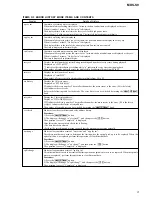
Page 2: ...hen an error occurs then issues a three or five digit code and an error message on the display If the code and message alternate find them in the following table and perform the indicated countermeasure Should the problem persist consult your nearest Sony dealer C11 Protected Take out the MD and close the record protect slot C12 Cannot Copy You tried to record a CD with a format that the external ...

Page 3: ...t errors Displayed as 0s ErrCd s indicates the history number The smaller the number the more recent is the error 00 is the latest indicates the error code Refer to the following table for the details The error history can be switched by turning the AMS knob retry adrs Display the 5 latest retry address Display as ss ADRS ss indicates the history number The smaller the number the more recent is th...

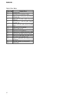
Page 4: ...d time 23 UTOC could be not read within the specified time 24 Content of UTOC is erroneous 30 Playing could not start 31 Content of sector is erroneous 40 Cause of retry occurred during normal recording 41 D RAM overflowed and retry was executed 42 Retry was executed during the writing to TOC 43 S F editing was interrupted by retry 50 Address could not be read except in access processing 51 Focusi...

Page 5: ...Notice that the minus side of a tantalum capacitor may be dam aged by heat Flexible Circuit Board Repairing Keep the temperature of the soldering iron around 270 C dur ing repairing Do not touch the soldering iron on the same conductor of the circuit board within 3 times Be careful not to apply force on the conductor when soldering or unsoldering This appliance is classified as a CLASS 1 LASER pro...

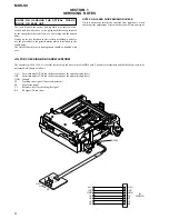
Page 6: ... FE RF I 3V IOP GND TE FE VC RF I 3V IOP GND TE FE VC RF 1 7 for MDM 7A NOTES ON HANDLING THE OPTICAL PICK UP BLOCK OR BASE UNIT The laser diode in the optical pick up block may suffer electro static break down because of the potential difference generated by the charged electrostatic load etc on clothing and the human body During repair pay attention to electrostatic break down and also use the p...

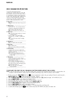
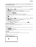
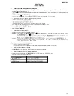
Page 7: ...complete Display Precedure 1 Whilepressingthe AMS knob and x button simultaneously connect the power plug to the outlet and release the AMS knob and x button simultaneously to display Check 2 Turn the AMS knob to display Service and press the YES button to display AUTO CHECK C01 3 Turn the AMS knob to display Iop Read C26 and press the YES button 4 is displayed and the recorded contents are displa...

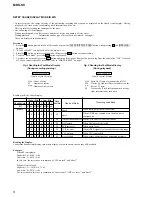
Page 8: ...es Number of retry errors Fig 2 Reading the Test Mode Display During playback Liquid crystal display Parts No Name of area named on TOC Cluster Address Physical address on the Sector disc Track mode Track information such as copy right information of each part Reading the Retry Cause Display 8 4 2 1 8 4 2 1 b7 b6 b5 b4 b3 b2 b1 b0 0 0 0 0 0 0 0 1 0 0 0 0 0 0 1 0 0 0 0 0 0 1 0 0 0 0 0 0 1 0 0 0 0 0...

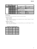
Page 9: ...ecimal display into binary display If more than two causes they will be added Example When 84 is displayed Higher bit 8 1000 t b7 Lower bit 4 0100 t b2 In this case as b2 and b7 are 1 and others are 0 it can be determined that the retry cause is combined of Emphasis OFF Monaural Original Copyright and Write allowed Example When 07 is displayed Higher bit 0 0000 t All 0 Lower bit 7 0111 t b0 b1 b2 ...

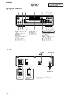
Page 10: ...7 YES 7 10 18 20 1 power STANDBY indicator 1 8 16 Z eject 5 8 17 m go back M go forward 9 16 17 18 24 z recording 0 8 10 x stop qa 7 8 16 NX play pause qs 8 16 BUTTON DESCRIPTIONS SECTION 2 GENERAL This section is extracted from instruction manual LOCATION OF CONTROLS Front Panel Back Panel AC power cord PC LINK to a wall outlet Amplifier etc CD player DBS tuner etc 1 1 Digital equipment with a DI...

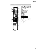
Page 11: ... 17 25 LEVEL qa 12 MENU NO w 10 18 20 MUSIC SYNC 8 14 NAME EDIT SELECT wa 24 PLAY MODE 2 16 REC MODE wg 9 REPEAT qd 16 SCROLL wd 17 T REC qj 13 YES 4 10 18 20 1 power 1 8 16 X pause 9 8 16 x stop 0 8 16 m fast reverse M fast forward qf 16 17 18 24 go back go forward qg 8 10 16 17 25 26 z recording qh 8 10 H play qk 8 16 A eject wh 8 17 Remote control BUTTON DESCRIPTIONS ...

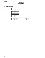
Page 12: ... S9 12 This set can be disassembled in the order shown below 3 1 DISASSEMBLY FLOW SECTION 3 DISASSEMBLY 3 2 CASE Page 13 Set 3 4 MAIN BOARD Page 14 3 3 MD MECHANISM DECK MDM 7A Page 13 3 5 BD BOARD Page 14 ...

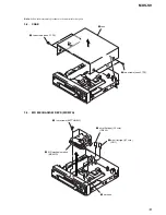
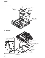
Page 13: ...Follow the disassembly procedure in the numerical order given 3 2 CASE 2 case 1 two screws case 3 TP2 1 two screws case 3 TP2 3 four screws BVTTWH M3 1 wire flat type 23 core CN400 1 wire flat type 27 core CN1 2 harness 4 MD mechanism deck MDM 7A ...

Page 14: ... BVTP3 8 5 MAIN board 1 wire flat type 15 core CN490 2 connector CN902 1 wire flat type 23 core CN103 2 wire flat type 27 core CN102 7 BD board 3 connector CN104 8 flexible board CN101 4 Remove five solders 5 Remove four solders BD board CONDUCTOR SIDE VIEW 6 two screws 2 6 ...

Page 15: ... of entering the test mode Procedure 1 While pressing the AMS knob and x button simultaneously connect the power plug to the outlet and release the AMS knob and x button When the test mode is set Check will be displayed Turning the AMS knob between the following three groups Tt Check Tt Service Tt Develop Tt Procedure 2 While pressing the AMS knob connect the power plug to the outlet and release t...

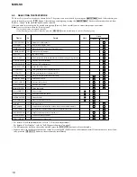
Page 16: ... release the mode immediately Display AUTO CHECK Err Display TEMP ADJUST LDPWRADJUST Iop Write Iop NV Save EF MO ADJUST EF CD ADJUST FBIAS ADJUST AG Set MO AG Set CD TEMP CHECK LDPWR CHECK EF MO CHECK EF CD CHECK FBIAS CHECK ScurveCHECK VERIFYMODE DETRK CHECK 0920 CHECK Iop Read Iop Compare ADJ CLEAR INFORMATION CPLAY1MODE CREC 1MODE Details Automatic self diagnosis Error history display clear Tem...

Page 17: ...recording position addresses 2 Changing the parts to be recorded 1 When the YES button is pressed during continuous recording the display changes as below When pressed another time the parts to be recorded can be changed REC goes off 2 When access completes the display changes to CREC 1 and REC lights up Note The numbers displayed shows you the recording position addresses 3 Ending the continuous ...

Page 18: ...UBQ address a Indicates the ADIP address Note is displayed when the address cannot be read MEANINGS OF OTHER DISPLAYS Mode display Error rate display Address display Auto gain display Not used in servicing Detrack check display Not used in servicing IVR display Not used in servicing C1 error and jitter display Not used in servicing AD error and jitter display Not used in servicing Servo OFF Tracki...

Page 19: ...check will start automatically 5 When XX CHECK is displayed the item corresponding to XX will be performed When 06 CHECK completes the disc loaded at step 3 will be ejected DISC IN will be displayed Load the check disc TDYS 1 6 When the disc is loaded in step 5 the check will automatically be resumed from 07 CHECK 7 After completing to test item 12 check OK or NG will be displayed If all items are...

Page 20: ...tc Start NG NG NG OK OK OK Laser Power Check 5 7 2 See page 23 5 7 3 See page 23 5 7 4 See page 24 Iop Compare Auto Check Replace optical pick up or MDM 7A 5 1 PARTS REPLACEMENT AND ADJUSTMENTS If malfunctions caused by optical pick up such as sound skipping are suspected follow the following check Check before replacement ...

Page 21: ... IS DIS PLAYED in 1 SERVICING NOTES See page 7 Abbreviation OP optical pick up 5 8 INITIAL SETTING OF ADJUSTMENT VALUE See page 26 5 10 TEMPERATURE COMPENSATION OFFSET ADJUSTMENT See page 26 5 11 LASER POWER ADJUSTMENT See page 26 5 13 TRAVERSE ADJUSTMENT See page 29 5 14 FOCUS BIAS ADJUSTMENT See page 30 5 17 AUTO GAIN CONTROL OUTPUT LEVEL ADJUSTMENT See page 29 op change in SELF DIAGNOSIS FUNCTI...

Page 22: ...ts and checks in Group Service of the test mode 3 Perform the adjustments to be needed in the order shown 4 Use the following tools and measuring devices Check Disc TDYS 1 Part No 4 963 646 01 Test Disk MDW 74 GA 1 Part No 4 229 747 01 Laser power meter LPM 8001 Part No J 2501 046 A or MD Laser power meter 8010S Part No J 2501 145 A 1 Oscilloscope Measure after performing CAL of prove Digital volt...

Page 23: ... up Connect the digital voltmeter to CN105 pin 1 I 3V and CN105 pin 2 IOP 2 Then turn the AMS knob to display LDPWR CHECK C13 3 Press the YES button once to display LD 0 9mW Check that the reading of the laser power meter become 0 85 to 0 91 mW KMS 260B or 0 90 to 0 96 mW KMS 260E 4 Press the YES button once more to display LD 7 0mW Check that the reading the laser power meter and digital voltmete...

Page 24: ...p is faulty In this case replace the optical pick up 5 7 5 Other Checks All the following checks are performed by the Auto Check mode They therefore need not be performed in normal operation 5 7 6 Traverse Check 5 7 7 Focus Bias Check 5 7 8 C PLAY Check 5 7 9 Self Recording Playback Check 5 7 6 Traverse Check Connection Procedure 1 Connect an oscilloscope to CN105 pin 4 TE and CN105 pin 6 VC on th...

Page 25: ...ton to display a Check that the C1 error is about 100 and ADER is below 2 9 Press the MENU NO button then press the Z button and take out the test disc MDW 74 GA 1 5 7 8 C PLAY Check MO Error Rate Check Procedure 1 Load the test disc MDW 74 GA 1 2 Turn the AMS knob to display CPLAY1MODE C34 3 Press the YES button to display CPLAY1MID 4 The display changes to C AD 5 If the C1 error rate is below 20...

Page 26: ...nd MENU NO button to display Iop Read C26 5 10 TEMPERATURE COMPENSATION OFFSET ADJUSTMENT Save the temperature data at that time in the non volatile memory as 25 C reference data Note 1 Usually do not perform this adjustment 2 Perform this adjustment in an ambient temperature of 22 C to 28 C Perform it immediately after the power is turned on when the internal temperature of the unit is the same a...

Page 27: ... pick up and when replacing the IC102 Otherwise the optical pick up check may deteriorate Note Perform this function with the optical pick up set at room temperature Procedure 1 Turn the AMS knob to display Iop NV Save C06 2 Press the YES button and display Iop stop 3 After the display changes to Iop xxsave press the YES button 5 13 TRAVERSE ADJUSTMENT Connection Procedure 1 Connect an oscilloscop...

Page 28: ...B SAVE for a mo ment and save the adjustment results in the non volatile memory Next EF CD ADJUST C08 will be displayed 19 Press the Z button and take out the check disc TDYS 1 Adjustment Location BD board see page 30 5 14 FOCUS BIAS ADJUSTMENT Procedure 1 Load the continuously recorded disc Refer to 5 6 USING THE CONTINUOUSLY RECORDED DISC See page 23 2 Turn the AMS knob to display CPLAY1MODE C34...

Page 29: ...ow 2 7 Press the YES button and display b T Check that the C1 error is below 100 and ADER is below 2 8 Press the YES button and display a T Check that the C1 error is below 100 and ADER is below 2 9 Press the MENU NO button then press the Z button and take out the disc Note If the C1 error and ADER are above other than the specified value at points a step 8 in the above or b step 7 in the above th...

Page 30: ...IC151 IC190 1 7 1 I 3V 2 IOP 3 GND 4 TE 5 FE 6 VC 7 RF BD BOARD Component Side BD BOARD Conductor Side Adjustment and checking Loacation Note It is useful to use the jig for checking BD board waveform Refer to Servicing Notes on page 6 ...

Page 31: ... XCAS OE WE RAS CAS D RAM IC153 DIN1 SYSTEM CONTROLLER IC1 1 2 HF MODULE ADDT DADT BCK LRCK Page 32 1024FS Page 32 Page 32 SWDT SCLK Page 32 TX0 CLIP REFLECT SW PROTECT SW LD LOW 5V 11 LIMIT IN REC SW S101 LIMIT IN OUT SW SIGNAL PATH PLAY ANALOG OUT REC ANALOG IN REC DIGITAL IN S105 REC POSITION S103 PACK OUT PLAY SW S104 PLAY POSITION S102 1 REFELECT RATE DETECT S102 2 PROTECT DETECT 1 S102 2 XBC...

Page 32: ...4 3 3V REGULATOR Q356 D421 D422 BT420 LITHUM BATTERY 5V 3 3V MD MECHANISM DECK SECTION BACK UP 3 3V SYSTEM 3 3V SYSTEM CONTROLLER IC1 2 2 A Page 31 B Page 31 D Page 31 C Page 31 L R L R ANALOG IN ANALOG OUT EEPROM IC195 RECT D461 462 RECT D471 472 D476 477 LOADING MOTOR DRIVER IC440 B UNREG 12V UNREG 12V ANALOG LINE OUT CIRCUIT 32V FL LED DRIVER IC761 B AC TO FL771 TR900 SUB POWER TRANSFORMER LINE...

Page 33: ...tion tolerances Waveforms are taken with a oscilloscope Voltage variations may be noted due to normal produc tion tolerances Circled numbers refer to waveforms Signal path E PLAY ANALOG OUT j REC ANALOG IN l REC DIGITAL IN Indication of transistor C B These are omitted E Q B These are omitted C E Q B These are omitted C E Q Note The components identified by mark 0 or dotted line with mark 0 are cr...

Page 34: ... OSCI 15 TX 14 XINT 13 RECP 12 DQSY 11 SQSY 10 XRST 9 SENS 8 SRDT 7 XLAT 6 SCLK 5 SWDT 4 MNT3 3 MNT2 2 MNT1 1 MNT0 PWM GENERATOR AUTO SEQUENCER SERVO DSP CPU I F MONITOR CONTROL SPINDLE SERVO EACH BLOCK EACH BLOCK DIGITAL AUDIO I F SAMPLING RATE CONVERTER CLOCK GENERATOR SUBCODE PROCESSOR EACH BLOCK A D CONVERTER ANALOG MUX EFM ACIRC ENCODER DECODER PLL SHOCK RESISTANT MEMORY CONTROLLER ATRAC ENCO...

Page 35: ...d Semiconductor Location Ref No Location D101 A 1 Q101 B 1 Q131 C 1 Q132 B 1 Q133 B 1 Q134 C 1 IC181 D 3 IC190 D 1 IC195 D 2 Q121 B 3 Q122 B 3 Q181 D 3 Q182 D 3 Ref No Location Ref No Location D181 D 3 D183 D 3 IC101 A 3 IC102 B 3 IC141 C 1 IC151 C 2 IC153 C 3 IC171 D 2 Semiconductor Location PACK OUT PLAY POSITION REC POSITION 22 22 BD BOARD FLEXIBLE BOARD COMPONENT SIDE 2B 1B 2C 1C Page 38 Page ...

Page 36: ...IAGRAM BD Board 1 2 See page 43 for Waveforms See page 33 for IC Block Diagrams The components identified by mark 0 or dotted line with mark 0 are critical for safety Replace only with part number specified Page 37 Page 37 Page 37 ...

Page 37: ...MDS S9 37 37 6 6 SCHEMATIC DIAGRAM BD Board 2 2 See page 43 for Waveforms See page 33 for IC Block Diagram Page 36 Page 36 Page 36 Page 40 Page 41 ...

Page 38: ... C502 R380 C261 C553 R515 C552 R552 R551 R272 R271 R264 R263 R514 R513 R512 R262 R261 R265 R266 R165 R164 R163 R162 R161 R166 R172 C271 C266 C272 R171 R277 D412 R276 D422 R177 R176 Q444 R421 C39 D421 C172 C151 R253 R153 R381 R151 R181 Q281 Q180 R280 R278 R252 R152 R178 R251 D155 D403 C484 FB803 R1002 R16 IC1 D404 R36 R37 MAIN BOARD COMPONENT SIDE A A A E E K K K E E E 1 1 2 26 27 2 22 23 B BD BOAR...

Page 39: ...56 C351 CN420 C252 C152 C461 C476 R L R L ANALOG OPTICAL IN IN OUT IC611 PC LINK J800 1 3 MAIN BOARD CONDUCTOR SIDE R306 R301 4 2 2 1 1 3 6 5 SHORT SOCKET E E 10 1 10 1 1 5 1 677 830 25 25 D PT BOARD CN901 1 13 A B C D E 1 2 3 4 5 6 7 8 6 8 PRINTED WIRING BOARD MAIN Board Conductor Side Semiconductor Location Ref No Location D461 C 8 D462 C 8 D471 D 8 D472 C 8 D476 D 8 D477 C 8 D481 D 8 IC400 B 8 ...

Page 40: ...MDS S9 40 40 6 9 SCHEMATIC DIAGRAM MAIN Board 1 3 See page 43 for Waveform Page 37 Page 42 Page 45 Page 41 Page 42 ...

Page 41: ...MDS S9 41 41 6 10 SCHEMATIC DIAGRAM MAIN Board 2 3 See page 43 for Waveforms See page 33 for IC Block Diagram Page 37 Page 40 Page 42 ...

Page 42: ...CHEMATIC DIAGRAM MAIN 3 3 PT Boards See page 33 for IC Block Diagrams The components identified by mark 0 or dotted line with mark 0 are critical for safety Replace only with part number specified Page 40 Page 40 Page 41 ...

Page 43: ...BOARD CN902 CHASSIS 6 12 PRINTED WIRING BOARD PT Board Page 39 3 3 Vp p 354 ns 3 6 Vp p 22 7 µs 1 4 Vp p 22 2 ns 4 4 Vp p 354 ns 2 9 Vp p 100 ns 3 6 Vp p 22 2 ns 4 2 Vp p 22 7 µs 5 2 Vp p 22 2 ns 0 6 Vp p 0 1 Vp p 0 5 Vp p Waveforms BD Board 1 IC101 1 I 2 J MD Play mode 6 IC151 wk XBCK 3 IC500 9 XTI 2 IC101 4 A MD Play mode 4 IC500 qa LRCK 3 IC101 8 E 9 F MD Play mode 7 IC171 3 5 IC500 qs BICK 4 I...

Page 44: ...8 JW710 JW711 JW712 JW713 JW714 JW715 JW716 JW717 JW718 JW719 JW720 JW721 JW722 JW723 JW724 JW725 IC761 C773 C770 E 3 1 E E DISPLAY BOARD CHASSIS CLEAR MENU NO YES M u z x m 1 3 5 4 Z C MAIN BOARD CN490 AMS PUSH ENTER S713 ROTARY ENCODER S701 705 S711 712 S714 715 S721 724 726 MDLP INPUT I 1 REC MODE STANDBY PLAY MODE LEVEL DISPLAY CHAR 1 681 805 11 11 A B C 1 2 3 4 5 6 7 8 9 10 11 6 13 PRINTED WI...

Page 45: ... 07GS K 10 50V 10 50V S1 S2 S3 S4 S5 S6 S7 S8 S9 S10 S11 S12 S13 S14 S15 S16 S17 S18 S19 S20 S21 S22 S23 S24 S25 S26 S27 S28 S29 S30 S31 S32 S33 S34 S35 G1 G2 G3 G4 G5 G6 G7 G8 G9 G10 G11 G12 G1 G2 G3 G4 S1 S2 S3 S4 S5 S6 S7 S8 S9 S10 S11 S12 S13 S14 S15 S16 S17 S18 S19 S20 S21 S22 S23 S24 S25 S26 S27 S28 G5 G6 G7 G8 G9 G10 G11 G12 G13 G13 S29 S30 S31 S32 S33 S34 S35 RMC KEY2 KEY1 KEY0 JOG1 JOG0 P...

Page 46: ... is on L NG Not used open 2 MNT1 SHOCK O Track jump detection signal output to the system controller IC1 3 MNT2 XBUSY O Busy monitor signal output to the system controller IC1 4 MNT3 SLOCK O Spindle servo lock status monitor signal output terminal Not used open 5 SWDT I Writing serial data signal input from the system controller IC1 6 SCLK I S Serial data transfer clock signal input from the syste...

Page 47: ... input terminal fixed at H in this set 72 ADRB I A A D converter operational range lower limit voltage input terminal fixed at L in this set 73 AVSS Ground terminal analog system 74 SE I A Sled error signal input from the CXA2523AR IC101 75 TE I A Tracking error signal input from the CXA2523AR IC101 76 DCHG I A Connected to the 3 3V power supply 77 TEST4 I Input terminal for the test Not used fixe...

Page 48: ...S IC141 95 FGIN I S 96 TEST1 I 97 TEST2 I 98 TEST3 I 99 DVSS Ground terminal digital system 100 EFMO O EFM signal output terminal when recording mode I S stands for schmitt input I A for analog input O 3 for 3 state output and O A for analog output in the column I O Input terminal for the test fixed at L ...

Page 49: ... terminal 17 XCIN I Sub system clock input terminal 32 768 kHz Not used open 18 XCOUT O Sub system clock output terminal 32 768 kHz Not used open 19 RESET I System reset signal input from the regulator IC400 L reset For several hundreds msec after the power supply rises L is input then it changes to H 20 XOUT O Main system clock output terminal 10 MHz 21 VSS Ground terminal 22 XIN I Main system cl...

Page 50: ...tection signal input from the playback position of over write head HR901 detect switch S104 L playback mode 50 XLATCH O Serial data latch pulse signal output to the CXD2662R IC151 51 OUT SW I Detection signal input from the loading out detect switch S103 L at a load out position others H 52 RDY O Not used open 53 ALE O Not used open 54 HOLD O Not used open 55 HLDA O Not used open 56 MNT2 XBUSY I B...

Page 51: ...signal output terminal for the beep sound drive Not used open 127 COAX OPT O Optical in or coaxial in selection signal output terminal L optical in H coaxial in Not used open 128 FL CS O Chip select signal output to the fluorescent indicator tube LED driver IC761 129 I2CPOWER I Power supply detection signal input from the IIC bus 130 VSS Ground terminal 131 STB O Relay drive signal output for the ...

Page 52: ...e components identified by mark 0 or dotted line with mark 0 are critical for safety Replace only with part number specified Ref No Part No Description Remark Ref No Part No Description Remark 1 1 681 806 11 PT BOARD 2 4 228 643 11 SCREW BVTTWH M3 STEP 3 3 363 099 21 SCREW CASE 3 TP2 4 4 229 363 51 CASE 5 1 792 811 11 WIRE FLAT TYPE 23 CORE 6 1 792 812 11 WIRE FLAT TYPE 27 CORE 07 1 777 071 61 COR...

Page 53: ...art No Description Remark 51 4 235 123 01 KNOB AMS 53 X 4953 948 1 PANEL ASSY FRONT 54 4 228 630 01 SPRING LID TENSION COIL 55 4 228 629 62 LID MD 57 A 4726 238 A DISPLAY BOARD COMPLETE 58 1 792 813 11 WIRE FLAT TYPE 15 CORE not supplied not supplied 53 54 55 5 51 4 58 56 56 57 ...

Page 54: ...T ASSY LEAF 309 A 4680 638 A LOCK HOLDER 310 4 229 533 02 SPRING STOPPER TORSION 311 4 227 012 01 SPRING HOLDER TENSION 312 4 227 019 03 PLATE HOLDER ASSY RETAINER 313 4 227 013 01 SPRING EJ TENSION 314 4 226 995 01 SLIDER EJ 315 4 226 996 03 LIMITTER EJ 316 4 226 997 04 SLIDER 317 4 226 998 01 LEVER CHG 318 4 227 006 01 GEAR SA 319 A 4735 075 A HOLDER ASSY 320 4 226 994 01 GUIDE L 321 A 4680 638 ...

Page 55: ...2 4 232 270 01 SCREW 1 7X3 5 PWH 363 4 226 990 01 BASE BU A 364 4 227 023 01 SPRING SPINDLE TORSION 365 4 227 004 01 GEAR LC 366 4 227 005 01 GEAR LD 367 4 227 008 01 GEAR SC 368 4 227 009 01 GEAR SD HR901 1 500 670 11 HEAD OVER WRITE M101 A 4672 898 A MOTOR ASSY SPINDLE M102 A 4735 076 A MOTOR ASSY SLED M103 A 4735 074 A MOTOR ASSY LOADING S102 1 771 957 11 SWITCH PUSH 2 KEY REFLECT RATE DETECT P...

Page 56: ...onents used on the set XX and X mean standardized parts so they may have some difference from the original one RESISTORS All resistors are in ohms METAL Metal film resistor METAL OXIDE Metal oxide film resistor F nonflammable Items marked are not stocked since they are seldom required for routine service Some delay should be anticipated when order ing these items SEMICONDUCTORS In each case u µ fo...

Page 57: ...AL CHIP 10K 5 1 16W R116 1 216 839 11 METAL CHIP 33K 5 1 16W R117 1 216 837 11 METAL CHIP 22K 5 1 16W R118 1 218 855 11 METAL CHIP 2 2K 0 5 1 16W R119 1 218 863 11 METAL CHIP 4 7K 0 5 1 16W R120 1 218 889 11 METAL CHIP 56K 0 5 1 16W R121 1 218 863 11 METAL CHIP 4 7K 0 5 1 16W R122 1 218 855 11 METAL CHIP 2 2K 0 5 1 16W R123 1 216 819 11 METAL CHIP 680 5 1 16W R124 1 216 809 11 METAL CHIP 100 5 1 1...

Page 58: ...247 843 11 CARBON 3 3K 5 1 4W R724 1 249 425 11 CARBON 4 7K 5 1 4W R726 1 249 437 11 CARBON 47K 5 1 4W R751 1 249 409 11 CARBON 220 5 1 4W R760 1 247 807 31 CARBON 100 5 1 4W R761 1 247 807 31 CARBON 100 5 1 4W R762 1 247 807 31 CARBON 100 5 1 4W R763 1 247 807 31 CARBON 100 5 1 4W R767 1 249 441 11 CARBON 100K 5 1 4W R769 1 247 843 11 CARBON 3 3K 5 1 4W R775 1 249 409 11 CARBON 220 5 1 4W R781 1 ...

Page 59: ...0 1 126 934 11 ELECT 220uF 20 10V C522 1 164 156 11 CERAMIC CHIP 0 1uF 25V C523 1 104 665 11 ELECT 100uF 20 10V C524 1 164 156 11 CERAMIC CHIP 0 1uF 25V C550 1 104 665 11 ELECT 100uF 20 10V C551 1 164 156 11 CERAMIC CHIP 0 1uF 25V C552 1 162 912 11 CERAMIC CHIP 7PF 0 5PF 50V C553 1 162 912 11 CERAMIC CHIP 7PF 0 5PF 50V C554 1 164 156 11 CERAMIC CHIP 0 1uF 25V C601 1 164 156 11 CERAMIC CHIP 0 1uF 2...

Page 60: ...5 1 16W R151 1 216 839 11 METAL CHIP 33K 5 1 16W R152 1 216 835 11 METAL CHIP 15K 5 1 16W R153 1 216 849 11 METAL CHIP 220K 5 1 16W R155 1 216 805 11 METAL CHIP 47 5 1 16W R161 1 216 833 11 METAL CHIP 10K 5 1 16W R162 1 216 833 11 METAL CHIP 10K 5 1 16W R163 1 216 833 11 METAL CHIP 10K 5 1 16W R164 1 216 833 11 METAL CHIP 10K 5 1 16W R165 1 218 724 11 METAL CHIP 22K 0 5 1 16W R166 1 218 724 11 MET...

Page 61: ... 0 1uF 50V C924 1 164 159 11 CERAMIC 0 1uF 50V C950 1 164 159 11 CERAMIC 0 1uF 50V C951 1 164 159 11 CERAMIC 0 1uF 50V C952 1 164 159 11 CERAMIC 0 1uF 50V CONNECTOR CN900 1 580 230 11 PIN CONNECTOR PC BOARD 2P DIODE D910 8 719 911 19 DIODE 1SS119 25 LINE FILTER 0LF900 1 419 625 11 COIL LINE FILTER LEAD LP900 1 690 880 31 LEAD WITH CONNECTOR RELAY 0RY910 1 755 356 11 RELAY TRANSFORMER 0TR950 1 435 ...

Page 62: ...ORY Clicking the version allows you to jump to the revised page Also clicking the version at the upper right on the revised page allows you to jump to the next revised page Ver Date Description of Revision 1 0 2001 06 New ...

Reviews: