background image

12

MZ-E501

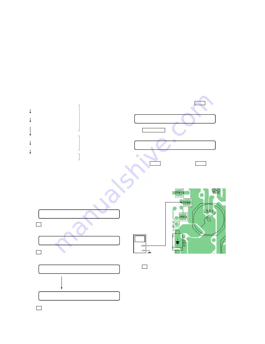
5-4.  MANUAL POWER ADJUSTMENTS

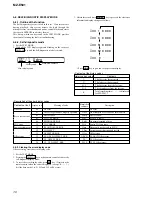
5-4-1. Adjustment sequence

The adjustments should be always performed in the following
sequence:

1

 Vc PWM Duty (L) adjustment (item No.:762)

 r

2

 Vc PWM Duty (H) adjustment (item No.:763)

 r

3

 VLL PWM Duty adjustment (item No.:764)

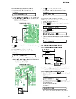
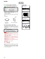
5-4-2.  Vc PWM Duty (L) adjustment method

1. Confirm that the power voltage is at 1.5 V DC.

2. Set the TEST MODE.

3. To set the overall adjustment mode, press VOL–  key.

LCD display

4. Press  PLAY MODE  key, and item No. will change to 762.

LCD display

SECTION 5

ELECTRICAL ADJUSTMENTS

5-1. GENERAL

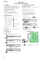
In this set, CD and MO discs can be automatically adjusted by setting
the Overall Adjustment mode within the TEST MODE,
Before performing these automatic adjustments, it is necessary to
clear the memory and adjust the power in the Manual mode.

5-2.  NOTES FOR ADJUSTMENT

5-2-1.  Jigs

• CD disc

TDYS-1 (part code: 4-963-646-01)

• MO disc

PTDM-1 (part code: J-2501-054-A)
or commercially available MO disc (recorded)

• Digital voltmeter

5-2-2. Adjustment sequence

The adjustments should be always performed in the following
sequence:

5-2-3.  Power

The power is supplied with 1.5 V DC from the battery case.

5-3. RESET NV

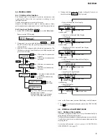
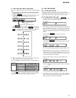
5-3-1.  How to reset NV

1. Set the TEST MODE.

2. Set the Manual mode and set the item No. 021, Reset NV.

LCD display

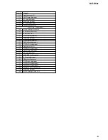
1

 Reset NV (Clear the memory)

2

 Manual power adjustments

3


Electrical offset adjustments

     (Do not enter the disc)

4

 Overall CD adjustments

5

 Overall MO adjustments

6


RESUME clear

Overall adjustment mode

Manual mode

Manual mode

3. Press  

X

  key on the remote control.

LCD display

4. Press  

X

  key on the remote control again.

LCD display

5. Press  

x

  key to terminate the Manual mode and return to the

TEST MODE.

021


Res NV CC

021


Res OK?

021


Res ***

021


Reset!

After reset is completed.

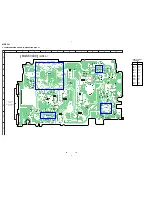
5. Connect a digital voltmeter to TP901 (VC) on the main board

and adjust VOL+  key (voltage up) and  VOL–  key (voltage
down) on the remote control.

Adjustment value:2.36V
Standard value:2.35 to 2.365V

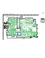
MAIN BOARD (SIDE B)

762


VclPWM XX

6. Press  

X

  key to write the adjustment value. Item No.will change

to 763.

000


Assy 

00

TP901 (VC)

digital voltmeter

Summary of Contents for MZ-E501

Page 1: ...l channel Frequency response 20 to 20 000 Hz 3 dB Wow and Flutter Below measurable limits Outputs Headphones earphones stereo mini jack maximum output level 5 mW 5 mW load impedance 16 ohms Power requirements Nickel Cadmium rechargeable battery One NC 6WM supplied 1 2V 600 mAh One LR6 size AA battery not supplied External power jack Power rating 3V DC AC power adaptor for the battery charging stan...

Page 2: ...LF indicating the solder contains no lead Caution Some printed circuit boards may not come printed with the lead free mark due to their particular size LEAD FREE MARK Unleaded solder has the following characteristics Unleaded solder melts at a temperature about 40 C higher than ordinary solder Ordinary soldering irons can be used but the iron tip has to be applied to the solder joint for a slightl...

Page 3: ... to electrostatic break down and also use the procedure in the printed matter which is included in the repair parts The flexible board is easily damaged and should be handled with care NOTES ON LASER DIODE EMISSION CHECK Never look into the laser diode emission from right above when checking it for adjustment It is feared that you will lose your sight NOTES ON HANDLING THE OPTICAL PICK UP BLOCK LC...

Page 4: ...ION 2 GENERAL LOCATION AND FUNCTION OF CONTROLS N VOL GROUP x x X 1N VOL VOL 3 Color Info LED N VOL HOLD DISPLAY SOUND PLAYMODE RPT ENT x GROUP HOLD 3 Color Info LED This section is extracted from instruction manual ...

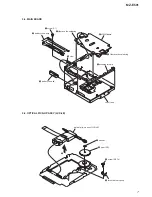
Page 5: ...n the numerical order given 3 1 CASE ASSY HOLDER ASSY SECTION 3 DISASSEMBLY Optical pick up assy LCX 4E Mechanism deck Case assy Holder assy Set Bracket assy MAIN board case assy 1 screws 1 4 MI 3 Move it away from the projection case rear hold assy 2 1 screws 1 4 MI 3 Move it away from the projection ...

Page 6: ...E501 3 3 BRACKET ASSY 3 screw 1 7 1 screw 1 7 2 bracket R assy 4 bracket L assy 3 2 MECHANISM DECK 4 mechanism deck 1 step screw MD 5 OP FLEXIBLE board CN501 6 MOTER FLEXIBLE board CN551 3 claw 2 claw 3 claw ...

Page 7: ... ASSY LCX 4E case rear 3 battery case lid 2 claw 5 Remove the soldering 6 MAIN board 5 Remove the soldering 4 ornamental strip 7 battery case assy 1 screw 1 7 optical pick up assy LCX 4E 3 screw MI 1 4 5 4 thrust detent spring 2 gear SA 1 washer ...

Page 8: ...E To set the TEST MODE two methods are available 1 Solder bridge and short TAP601 TEST on the main board Then turn on the power Press the x button or close the upper panel MAIN BOARD SIDE B 2 In the normal mode operate the keys on the set and those on the remote control rapidly as specified below Turn on HOLD switch on the set Holding down x STOP key on the set press the keys on the remote control...

Page 9: ...4 2 How to set the Manual mode 1 Set theTEST MODE and press VOL key to set the Manual mode Remote control LCD display 4 During each test mode the display is changed from one to another each time DISPLAY key is pressed Address Adjusted Value Display LCD display Jitter Value Adjusted Value Display LCD display Block Error Value Adjusted Value Display LCD display ADIP Error Value Adjusted Value Displa...

Page 10: ...e N 2 The second error from the last one R Total recording time is displayed for MZ E501 Description No error An attempt to access an abnormal address HIGH TEMP Focus off center Abnormal rotation of disc Faulty TOC contents Data could not be read at SYNC Instantaneous interruption detected Offset error FE ABCD Offset error TE Offset error X1 TE Offset error Description of the error display codes M...

Page 11: ...re considered as OK LCD display 4 When all the key have been checked or when the top panel is opened during this checking the system terminates the Key Check mode and return to the TEST MODE 000 0F 4 7 Sound Skip Check Result Display Mode This set can display and check the error count occurring during play Setting method of Sound Skip Check Result Display Mode 1 Setting the test mode 2 Pressing th...

Page 12: ...O disc recorded Digital voltmeter 5 2 2 Adjustment sequence The adjustments should be always performed in the following sequence 5 2 3 Power The power is supplied with 1 5 V DC from the battery case 5 3 RESET NV 5 3 1 How to reset NV 1 Set the TEST MODE 2 Set the Manual mode and set the item No 021 Reset NV LCD display 1 Reset NV Clear the memory 2 Manual power adjustments 3 Electrical offset adju...

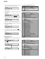
Page 13: ...justment mode Automatic adjustments are made LCD display XXX Item No for which an adjustment is being executed 5 4 3 Vc PWM Duty H adjustment method 1 Set the Manual mode and set the item No to 763 LCD display 2 Connect a digital voltmeter to TP901 VC on the main board and adjust VOL key and VOL key on the remote control Adjustment value 2 75V Standard value 2 74 to 2 755V MAIN BOARD SIDE B 3 Pres...

Page 14: ... ON OFF electrical offset difference measurement Item No 030 035 Completed 2 Overall CD adjustment items Contents VC VR power voltage High Low selection HPIT setting Sarvo OFF SLED move to inside SLED move to outside High reflection CD electrical offset adjustment Laser ON Focus UP VC correction ALFA offset adjustment IJ offset adjustment FE offset adjustment HPIT adjustment Focus servo ON TE offs...

Page 15: ...N offset adjustment TEIN offset adjustment TWPP offset adjustment Tracking servo ON TWPP offset adjustment ABCD gain adjustment KF gain adjustment ADIP BPF fo adjustment FCS gain adjustment TRK gain adjustment TWPP gain adjustment TWPP offset adjustment 1 TWPP offset adjustment 2 TWPP OP offset adjustment RF gain adjustment R GRV setting Servo OFF Item No 230 236 237 238 244 245 100 562 120 122 12...

Page 16: ...ed numbers refer to waveforms Signal path F Audio Analog J Audio Digital Replacement of IC601 used in this set requires a special tool The voltage and waveform of CSP chip size package cannot be measured because its lead layout is different from that of conventional IC Note on Printed Wiring Boards MAIN SECTION X parts extracted from the component side Pattern from the side which enables seeing Th...

Page 17: ... 18 19 LASER AUTO POWER CONTROL Q501 3 4 2 19 11 20 13 12 5 18 9 10 14 15 16 17 7 8 6 1 TRACKING COIL FOCUS COIL 20 Jx Jy Jx Ix Iy Iy Ix Jx Jy A B C D PD Ix a F b c d MINIDISC OPTICAL PICK UP BLOCK LCX 4E LD AVCC S0 S1 AVCC S0 LD K LD A MON D C B A Jy Jx Ix Iy D D C PD I PD O C B A VREF VREF A C Jy Jx Ix Iy S1 RF AMP FOCUS ERROR TRACKING ERROR TPP WPP APC SERIAL I F VL 22 40 DVDD AVCC VIF RF OUT P...

Page 18: ...O F F O N DRY BATTERY SIZE AA IEC DESIGNATION LR6 1PC 1 5V 1 681 868 11 11 11 11 MAIN BOARD SIDE A 1 2 A B C D E F G 3 4 5 6 7 8 9 10 6 2 PRINTED WIRING BOARD MAIN SECTION SIDE A Ref No Location D101 C 9 D201 C 10 D801 E 7 D855 D 10 D902 F 9 D903 F 10 IC301 B 9 IC501 F 4 IC601 B 4 IC901 E 9 Q301 A 8 Q501 F 3 Semiconductor Location ...

Page 19: ... MOTOR FLEXIBLE BOARD M901 SPINDLE MOTOR M902 SLED MOTOR S809 OPEN CLOSE DETECT SWITCH PICK UP OPTICAL BLOCK LCX 4E J301 1 681 868 11 11 C609 TP901 VC TP904 VL TAP601 TEST 1 2 A B C D E F G 3 4 5 6 7 8 9 10 6 3 PRINTED WIRING BOARD MAIN SECTION SIDE B Ref No Location D901 E 2 IC551 F 5 IC801 B 9 Q801 C 3 Semiconductor Location ...

Page 20: ...20 20 MZ E501 OPR_LED_G_H OPR_LED_G_L OPR_LED_R_H OPR_LED_R_L TAP602 6 4 SCHEMATIC DIAGRAM MAIN SECTION 1 3 See page 16 for Waveforms See page 25 26 for IC Pin Function Description ...

Page 21: ...21 21 MZ E501 IC B D IC B D C956 0 1 6 5 SCHEMATIC DIAGRAM MAIN SECTION 2 3 See page 23 24 for IC Block Diagrams ...

Page 22: ...22 22 MZ E501 IC B D INFO 6 6 SCHEMATIC DIAGRAM MAIN SECTION 3 3 See page 23 for IC Block Diagrams ...

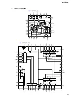
Page 23: ...12 VM2 PGNDW WO VMVW VO PGNDUV UO VMU GND2 CPW1 CPV1 CPU1 COM CPWO CPVO 3 PHASE CONTROL BIAS VC PRE DRIVER PRE DRIVER H BRIDGE CONTROL H BRIDGE CONTROL VC VG VC VG VC VC VC VG PRE DRIVER PRE DRIVER H BRIDGE CONTROL H BRIDGE CONTROL VC VG VC VG VC VG VC VC PRE DRIVER IC551 SC111257FCR2 V REF MT SW BST SW BEEP 19 20 21 22 23 24 18 17 16 15 14 13 PW SW 12 11 10 8 7 BST1 9 BST2 6 5 4 3 2 1 BST AGC PW ...

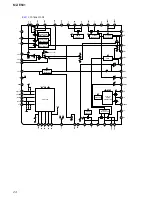
Page 24: ... 48 47 46 45 44 43 L1 RF1 INM1 DTC1 DTC2 RF2 INM2 PWM1 PWM2 VG LG PGND2 L2 NC NC VD VC2 XRST CRST RSTREF VREF VB GND CLKSEL VAIFON FFCLR SLEEP CLK SERIAL PASS REGULATOR VA SERIAL PASS REGULATOR VD SERIAL PASS REGULATOR VIF BANDGAP REFERENCE VC XRST INT VC VC VSTB VC VB POWER SWITCH 1 VG STEP UP PRE DRIVEER VG STEP UP PRE DRIVEER PWM VG VC VG VG VC STEP UP DC DC CONVERTOR START UP VC VB VB VG VG ST...

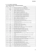
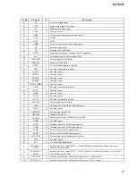
Page 25: ...ght amount monitor input terminal non invert input 20 PD O O Light amount monitor output terminal 21 ADIP O ADIP duplex FM signal 66 15kHz 3kHz output to the system controller IC601 22 DVDD I Power supply terminal 1 9V digital system 23 SBUS I O SSB serial data input output with the system controller IC601 24 SCK I SSB serial clock signal input from the system controller IC601 25 XRST I Reset sign...

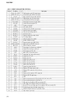
Page 26: ...CI I Input to the X tal oscillator circuit 25 OSCO O Output from the X tal oscillator circuit 26 VSIOSC Ground for OSC cell 27 DAVDD Built in DAC VCC 28 VREFL Built in DAC VREF L ch 29 AOUTL O Built in DAC L ch output 30 AOUTR O Built in DAC R ch output 31 VREFR I Built in DAC VREF R ch 32 DAVSS Ground for the built in DAC 33 ASYO O Playback EFM duplex signal output 34 ASYI I Playback EFM comparis...

Page 27: ... used open 71 FS256 O Not used open 72 MVCI I Not used connected to ground 73 DSPVDD1 Power supply for DSP block 74 ADFG I ADIP duplex FM signal 20 05 1KHz input 75 F0CNT O Not used open 76 DIFVDD0 Power supply for DSP I F 77 DIFVSS0 Ground for DSP I F 78 APCREF O Output to the reference PWM for the laser APC 79 LDDR O Not used open 80 TRDR O Tracking servo drive PWM signal output 81 TFDR O Tracki...

Page 28: ... MNT0 O DSP monitor output 0 107 MNT1 O DSP monitor output 1 108 MNT2 O DSP monitor output 2 109 MNT3 O DSP monitor output 3 110 SENSE O Not used open 111 TX O Not used open 112 RECP O Not used open 113 DSPVDD3 Power supply for DSP block 114 to 117 NC Not used open 118 DRAMVSS0 Ground for the external D RAM 119 DRAMVDD0 Power supply for the external D RAM 120 to 138 NC Not used open 139 DRAMVDD1 P...

Page 29: ...supply for the microcomputer I F block 177 MIFVSS1 Ground for the microcomputer I F block 178 AOUT SEL O HP LINE changeover signal output Not used open 179 SI0 I Serial data input CH0 180 SO0 O Serial data output CH0 181 SCK0 O Serial clock signal output CH0 182 XGUM ON I Not used open 183 BEEP O Beep sound output 191 OPT DET I Not used open 192 XJACK DET I Not used open 193 XMIC DET I Not used op...

Page 30: ...228 SYNC REC I Not used open 229 TSB_SSB_CTL O TSB SSB switching 230 PROTECT I Not used open 231 FLASHVDD Power supply for FLASH 232 FLASHVSS Ground terminal for FLASH 233 SLD MON I Sled monitor 234 VLON O Laser power supply control 235 SLEEP O SLEEP request 236 FFCLR O Input latch output for the start signal 237 CHG GAIN O Not used open 238 CHG O Not used open TUN REG ON O Not used open 241 MIFVD...

Page 31: ... TERMINAL ASSY BATTERY 3 3 232 180 01 BUTTON OPEN 4 3 224 025 01 TERMINAL BOARD MINUS 5 3 232 179 01 STRIP ORNAMENTAL SILVER 5 3 232 179 11 STRIP ORNAMENTAL PINK 5 3 232 179 21 STRIP ORNAMENTAL BLUE 5 3 232 179 31 STRIP ORNAMENTAL YELLOW 6 4 218 233 09 SCREW 1 4 MI 7 X 3380 870 1 HOLDER ASSY S 8 X 3380 740 1 LID ASSY UPPER SILVER 8 X 3380 741 1 LID ASSY UPPER PINK 8 X 3380 742 1 LID ASSY UPPER BLU...

Page 32: ...1 4 MI 59 4 222 208 01 GEAR SB 60 3 043 237 02 BEARING N 61 4 222 203 01 SCREW LEAD 062 X 3379 869 1 OPTICAL PICK UP ASSY LCX 4E 63 3 222 391 01 SPRING M RACK 64 3 225 278 11 SCREW TAPPING 65 X 3379 529 1 BASE ASSY MOTOR M901 8 835 706 01 MOTOR DC SSM18A C NP SPINDLE M902 1 763 399 11 MOTOR DC SLED WITH PULLY The components identified by mark 0 or dotted line with mark 0 are critical for safety Re...

Page 33: ...3000PF 10 10V C527 1 127 772 11 CERAMIC CHIP 33000PF 10 10V C529 1 135 259 11 TANTAL CHIP 10uF 20 00 6 3V C530 1 164 939 11 CERAMIC CHIP 0 0022uF 10 00 16V C551 1 125 837 11 CERAMIC CHIP 1uF 10 6 3V C552 1 125 837 11 CERAMIC CHIP 1uF 10 6 3V C557 1 127 772 11 CERAMIC CHIP 33000PF 10 10V C558 1 127 772 11 CERAMIC CHIP 33000PF 10 10V C559 1 127 772 11 CERAMIC CHIP 33000PF 10 10V C561 1 107 820 11 CE...

Page 34: ...ORT 0 R553 1 216 296 11 SHORT 0 R554 1 216 296 11 SHORT 0 R555 1 216 296 11 SHORT 0 R601 1 218 929 11 RES CHIP 10 5 1 16W R602 1 218 935 11 RES CHIP 33 5 1 16W R603 1 218 943 11 RES CHIP 150 5 1 16W R605 1 218 965 11 RES CHIP 10K 5 1 16W R606 1 218 977 11 RES CHIP 100K 5 1 16W R607 1 218 977 11 RES CHIP 100K 5 1 16W R609 1 218 981 11 RES CHIP 220K 5 1 16W R612 1 218 959 11 RES CHIP 3 3K 5 1 16W R6...

Page 35: ...al for safety Replace only with part number specified ACCESSORIES 1 251 895 11 BATTERY CASE 1 476 211 21 REMOTE CONTROL UNIT RM MC10L 0 1 476 277 11 ADAPTOR AC AC MZR55 Hong Kong 0 1 476 763 11 CHARGE UNIT Hong Kong 0 1 476 763 14 CHARGE UNIT AEP French 0 1 476 857 11 ADAPTOR AC AC ES305 AEP French 1 528 299 61 BATTERY NI CD NC 6WM 3 008 521 01 CASE BATTERY CHARGE 3 220 749 01 CASE CARRYING 3 231 ...

Page 36: ...36 MZ E501 MEMO ...
Page 37: ...MZ E501 AEP Model Hong Kong Model SERVICE MANUAL SUPPLEMENT 1 Ver 1 2 2001 12 Subject 1 Schematic diagram and printed wiring board are changed ECN DAB01214 ...

Page 38: ...iring board are changed Before change After change Part No Description 1 681 868 12 MAIN BORD Part No Description 1 681 868 11 MAIN BORD Location of parts code on changed printed wiring board MAIN BOARD SIDE B Before change 1 681 868 11 After change 1 681 868 12 ...

Page 39: ... 28 41 42 1 44 21 31 26 43 24 23 4 8 9 10 11 12 14 5 6 13 7 18 19 LASER AUTO POWER CONTROL Q501 3 4 2 19 11 20 13 12 5 18 9 10 14 15 16 17 7 8 6 1 TRACKING COIL FOCUS COIL 20 Jx Jy Jx Ix Iy Iy Ix Jx Jy A B C D PD Ix a F b c d MINIDISC OPTICAL PICK UP BLOCK LCX 4E LD AVCC S0 S1 AVCC S0 LD K LD A MON D C B A Jy Jx Ix Iy D D C PD I PD O C B A VREF VREF A C Jy Jx Ix Iy S1 RF AMP FOCUS ERROR TRACKING E...

Page 40: ...11 Q501 H 3 Q901 G 11 Q902 F 11 Q903 F 11 Semiconductor Location Note on Printed Wiring Boards X parts extracted from the component side Pattern from the side which enables seeing The other layers patterns are not indicated Caution Pattern face side Parts on the pattern face side seen from the Side B pattern face are indicated Parts face side Parts on the parts face side seen from the Side A parts...

Page 41: ...13 14 Ref No Location D901 F 3 IC551 H 6 IC801 C 12 IC903 H 5 Q801 D 4 Semiconductor Location Note on Printed Wiring Boards X parts extracted from the component side Pattern from the side which enables seeing The other layers patterns are not indicated Caution Pattern face side Parts on the pattern face side seen from the Side B pattern face are indicated Parts face side Parts on the parts face si...

Page 42: ... WAVEFORMS 1 2 3 4 Approx 12 mVp p X601 OSCO IC501 rs FE IC501 ed RF OUT IC501 1 TE Approx 1 2 Vp p Approx 10 mVp p 2 7 V 22 1 ns Voltages are taken with a VOM Input imped ance 10 MΩ Voltage variations may be noted due to normal production tolerances Waveforms are taken with a oscilloscope Voltage variations may be noted due to normal production tolerances Circled numbers refer to waveforms Signal...

Page 43: ...ors are in Ω and 1 4 W or less unless otherwise specified B Line Power voltage is dc 1 5V and fed with regulated dc power supply from battery terminal Voltages and waveforms are dc with respect to ground under no signal conditions no mark PLAY Voltages are taken with a VOM Input impedance 10 MΩ Voltage variations may be noted due to normal produc tion tolerances IC B D IC B D See page 9 10 for IC ...

Page 44: ...less unless otherwise specified C panel designation B Line Power voltage is dc 1 5V and fed with regulated dc power supply from battery terminal Voltages and waveforms are dc with respect to ground under no signal conditions no mark PLAY Voltages are taken with aVOM Input impedance 10 MΩ Voltage variations may be noted due to normal produc tion tolerances Signal path F Audio Analog J Audio Digital...

Page 45: ...12 VM2 PGNDW WO VMVW VO PGNDUV UO VMU GND2 CPW1 CPV1 CPU1 COM CPWO CPVO 3 PHASE CONTROL BIAS VC PRE DRIVER PRE DRIVER H BRIDGE CONTROL H BRIDGE CONTROL VC VG VC VG VC VC VC VG PRE DRIVER PRE DRIVER H BRIDGE CONTROL H BRIDGE CONTROL VC VG VC VG VC VG VC VC PRE DRIVER IC551 SC111257FCR2 V REF MT SW BST SW BEEP 19 20 21 22 23 24 18 17 16 15 14 13 PW SW 12 11 10 8 7 BST1 9 BST2 6 5 4 3 2 1 BST AGC PW ...

Page 46: ... 48 47 46 45 44 43 L1 RF1 INM1 DTC1 DTC2 RF2 INM2 PWM1 PWM2 VG LG PGND2 L2 NC NC VD VC2 XRST CRST RSTREF VREF VB GND CLKSEL VAIFON FFCLR SLEEP CLK SERIAL PASS REGULATOR VA SERIAL PASS REGULATOR VD SERIAL PASS REGULATOR VIF BANDGAP REFERENCE VC XRST INT VC VC VSTB VC VB POWER SWITCH 1 VG STEP UP PRE DRIVEER VG STEP UP PRE DRIVEER PWM VG VC VG VG VC STEP UP DC DC CONVERTOR START UP VC VB VB VG VG ST...

Page 47: ... NI I Light amount monitor input terminal non invert input 20 PD O O Light amount monitor output terminal 21 ADIP O ADIP duplex FM signal 66 15kHz 3kHz output to the system controller IC601 22 DVDD Power supply terminal 1 9V digital system 23 SBUS I O SSB serial data input output with the system controller IC601 24 SCK I SSB serial clock signal input from the system controller IC601 25 XRST I Rese...

Page 48: ...CI I Input to the X tal oscillator circuit 25 OSCO O Output from the X tal oscillator circuit 26 VSIOSC Ground for OSC cell 27 DAVDD Built in DAC VCC 28 VREFL Built in DAC VREF L ch 29 AOUTL O Built in DAC L ch output 30 AOUTR O Built in DAC R ch output 31 VREFR I Built in DAC VREF R ch 32 DAVSS Ground for the built in DAC 33 ASYO O Playback EFM duplex signal output 34 ASYI I Playback EFM comparis...

Page 49: ... used open 71 FS256 O Not used open 72 MVCI I Not used connected to ground 73 DSPVDD1 Power supply for DSP block 74 ADFG I ADIP duplex FM signal 20 05 1KHz input 75 F0CNT O Not used open 76 DIFVDD0 Power supply for DSP I F 77 DIFVSS0 Ground for DSP I F 78 APCREF O Output to the reference PWM for the laser APC 79 LDDR O Not used open 80 TRDR O Tracking servo drive PWM signal output 81 TFDR O Tracki...

Page 50: ...MNT0 O DSP monitor output 0 107 MNT1 O DSP monitor output 1 108 MNT2 O DSP monitor output 2 109 MNT3 O DSP monitor output 3 110 SENSE O Not used open 111 TX O Not used open 112 RECP O Not used open 113 DSPVDD3 Power supply for DSP block 114 to 117 NC Not used open 118 DRAMVSS0 Ground for the external D RAM 119 DRAMVDD0 Power supply for the external D RAM 120 to 138 NC Not used open 139 DRAMVDD1 Po...

Page 51: ...1 Power supply for the microcomputer I F block 177 MIFVSS1 Ground for the microcomputer I F block 178 AOUT SEL O HP LINE changeover signal output Not used open 179 SI0 I Serial data input CH0 180 SO0 O Serial data output CH0 181 SCK0 O Serial clock signal output CH0 182 XGUM ON I Not used open 183 BEEP O Beep sound output 191 OPT DET I Not used open 192 XJACK DET I Not used open 193 XMIC DET I Not...

Page 52: ...228 SYNC REC I Not used open 229 TSB_SSB_CTL O TSB SSB switching 230 PROTECT I Not used open 231 FLASHVDD Power supply for FLASH 232 FLASHVSS Ground terminal for FLASH 233 SLD MON I Sled monitor 234 VLON O Laser power supply control 235 SLEEP O SLEEP request 236 FFCLR O Input latch output for the start signal 237 CHG GAIN O Not used open 238 CHG O Not used open TUN REG ON O Not used open 241 MIFVD...

Page 53: ...00PF 10 10V C527 1 127 772 11 CERAMIC CHIP 33000PF 10 10V C529 1 135 259 11 TANTAL CHIP 10uF 20 00 6 3V C530 1 164 939 11 CERAMIC CHIP 0 0022uF 10 00 50V C551 1 125 837 11 CERAMIC CHIP 1uF 10 6 3V C552 1 125 837 11 CERAMIC CHIP 1uF 10 6 3V C557 1 127 772 11 CERAMIC CHIP 33000PF 10 10V C558 1 127 772 11 CERAMIC CHIP 33000PF 10 10V C559 1 127 772 11 CERAMIC CHIP 33000PF 10 10V C561 1 107 820 11 CERA...

Page 54: ... R505 1 208 691 11 METAL CHIP 2 2K 0 5 1 16W R515 1 208 691 11 METAL CHIP 2 2K 0 5 1 16W R516 1 208 691 11 METAL CHIP 2 2K 0 5 1 16W R517 1 208 691 11 METAL CHIP 2 2K 0 5 1 16W R519 1 218 977 11 RES CHIP 100K 5 1 16W R521 1 242 967 11 RES CHIP 1 5 1 16W R601 1 208 635 11 RES CHIP 10 5 1 16W R602 1 218 935 11 RES CHIP 33 5 1 16W R603 1 218 943 11 RES CHIP 150 5 1 16W R605 1 218 965 11 RES CHIP 10K ...

Page 55: ...2 1 233 973 11 RES NETWORK CHIP TYPE 100K RB553 1 233 967 11 RES NETWORK CHIP TYPE 10K SWITCH S801 1 786 033 21 SWITCH TACTILE x S802 1 786 033 21 SWITCH TACTILE N S803 1 786 033 21 SWITCH TACTILE S804 1 786 033 21 SWITCH TACTILE VOL S805 1 786 033 21 SWITCH TACTILE VOL S806 1 786 033 21 SWITCH TACTILE GROUP S808 1 762 078 11 SWITCH SLIDE HOLD S809 1 762 498 21 SWITCH PUSH 1 KEY OPEN CLOSE DETECT ...

Page 56: ...he upper right on the revised page allows you to jump to the next revised page Ver Date Description of Revision 1 2 2001 12 Supplement 1 Change of board 1 681 868 11 1 681 868 12 Correction of IC pin function description and exploded views 1 1 2001 11 AEP French model addition 1 0 2001 07 New ENG 01021 ECN DAB01214 ...

Reviews: