background image

– 2 –

SAFETY-RELATED COMPONENT WARNING!!

COMPONENTS IDENTIFIED BY MARK 

0

 OR DOTTED LINE WITH

MARK 

0

 ON THE SCHEMATIC DIAGRAMS AND IN THE PARTS

LIST ARE CRITICAL TO SAFE OPERATION.
REPLACE THESE COMPONENTS WITH SONY PARTS WHOSE
PART NUMBERS APPEAR AS SHOWN IN THIS MANUAL OR IN
SUPPLEMENTS PUBLISHED BY SONY.

Flexible Circuit Board Repairing

• Keep the temperature of the soldering iron around 270°C

during repairing.

• Do not touch the soldering iron on the same conductor of the

circuit board (within 3 times).

• Be careful not to apply force on the conductor when soldering

or unsoldering.

Notes on chip component replacement

• Never reuse a disconnected chip component.
• Notice that the minus side of a tantalum capacitor may be

damaged by heat.

Precautions for Laser Diode Emission Check

When checking the emission of the laser diode during adjust-
ments, never view directly downwards as this may lead to
blindness.

Precautions for Using Optical Pick-up

 (LCX-2E)

As the laser diode inside the optical pick-up damages by static
electricity easily, solder the laser tap of the Optical pick-up
flexible board when handling. Also take the necessary measures
to prevent damages by static electricity. Handle the Optical pick-
up flexible board with care as it breaks easily.

Laser tap

Optical Pick-up flexible board

CAUTION

Use of controls or adjustments or performance of procedures
other than those specified herein may result in hazardous
radiation exposure.

IN NO EVENT SHALL SELLER BE
LIABLE FOR ANY DIRECT,
INCIDENTAL OR CONSEQUENTIAL
DAMAGES OF ANY NATURE, OR
LOSSES OR EXPENSES RESULTING
FROM ANY DEFECTIVE PRODUCT
OR THE USE OF ANY PRODUCT.

“MD WALKMAN” is a trademark of Sony
Corporation.

This MiniDisc player is classi-
fied as a CLASS 1 LASER
product.
The CLASS 1 LASER
PRODUCT label is located on
the bottom exterior.

Dimensions

Approx. 81 

×

 25 

×

 74 mm (w/h/d)

(3 

1

/

4


×

 1 

×

 3 in.) not including projecting

parts and controls

Mass

Approx. 95 g (3.4 oz.) the player only
Approx. 136 g (4.8 oz.) incl. a premastered MD
and a LR6 (size AA) alkaline battery

Supplied accessories

Headphones with a remote control (1)
Carrying pouch (1)

Design and specifications are subject to change
without notice.

ATTENTION AU COMPOSANT AYANT RAPPORT

 À LA SÉCURITÉ!!

LES COMPOSANTS IDENTIFIÉS PAR UNE MARQUE 

0

 SUR LES

DIAGRAMMES SCHÉMATIQUES ET LA LISTE  DES PIÈCES
SONT CRITIQUES POUR LA SÉCURITÉ DE FONCTIONNEMENT.
NE REMPLACER CES COMPOSANTS QUE PAR DES PIÈCES
SONY DONT LES NUMÉROS SONT DONNÉS DANS CE MANUEL
OU DANS LES SUPPLÉMENTS PUBLIÉS PAR SONY.

Summary of Contents for MZ-E60

Page 1: ...e 20 to 20 000 Hz 3 dB Wow and Flutter Below measurable limit Outputs Headphones stereo mini jack maximum output level 5 mW 5 mW load impedance 16 ohms General Power requirements One LR6 size AA battery not supplied Battery operation time You can check the battery condition with the battery indication which is displayed while using the player t Battery power decreasing v r Weak battery v e The bat...

Page 2: ...event damages by static electricity Handle the Optical pick up flexible board with care as it breaks easily Laser tap Optical Pick up flexible board CAUTION Use of controls or adjustments or performance of procedures other than those specified herein may result in hazardous radiation exposure IN NO EVENT SHALL SELLER BE LIABLE FOR ANY DIRECT INCIDENTAL OR CONSEQUENTIAL DAMAGES OF ANY NATURE OR LOS...

Page 3: ...2 Adjustment Sequence 12 5 2 3 Power 12 5 3 Reset NV 12 5 3 1 How to Reset NV 12 5 4 Overall Adjustment Mode 12 5 4 1 Overall Adjustment Mode Structure 12 5 4 2 Overall CD and MO Adjustment Method 12 5 4 3 Overall CD and MO Adjustment Items 13 TABLE OF CONTENTS 6 DIAGRAMS 14 6 1 IC Pin Description 14 6 1 1 IC801 RU6915MF 0006 System Control 14 6 2 Block Diagrams 17 6 2 1 MD Block Diagram 17 6 2 2 ...

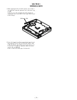
Page 4: ...e hook of the OPEN CLOSE switch MAIN board S809 with tape 2 This set is designed to perform automatic adjustment for each adjustment and write its value to EEPROM Therefore when EEPROM MAIN board IC802 has been replaced in service be sure to perform automatic adjustment and write resultant values to the new EEPROM Refer to section 4 Test Mode page 10 for details SECTION 1 SERVICING NOTE MAIN board...

Page 5: ... 5 SECTION 2 GENERAL This section is extracted from instruction manual ...

Page 6: ... 6 ...

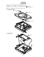
Page 7: ...N 3 DISASSEMBLY 3 1 PANEL ASSY UPPER 3 2 HOLDER ASSY Note Follow the disassembly procedure in the numerical order given Set Panel Assy Upper Holder Assy Mechanism Deck Service Assy OP Main Board 4 screws 1 4 MI 3 screws 1 4 MI 5 panel assy upper 1 2 2 shaft 3 holder assy 1 shaft ...

Page 8: ...BOARD 7 mechanism deck 1 sheet BLIND 6 CN551 5 CN501 claw 2 screw MD step 3 4 3 2 screws 1 7x2 5 1 screws 1 7x2 5 4 MAIN board knob HOLD S808 S806 S807 knobs MB Note When installing fit the knobs HOLD MB and the switchs S806 807 808 ...

Page 9: ... 9 3 7 SERVICE ASSY OP 4 M 1 4 3 M 1 4 1 washer 2 gear SA 5 service assy OP ...

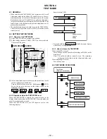
Page 10: ...s otherwise specified in the text the key means that on the remote control 4 2 SETTINGTHE TEST MODE 4 2 1 How to set the TEST MODE To set the TEST MODE two methods are available 1 Solder bridge and short TAP801 TEST on the main board Then turn on the power 2 In the normal mode operate the keys on the set and those on the remote control as specified below Turn on HOLD switch on the set Holding down...

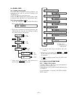
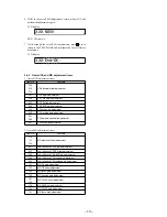
Page 11: ...erforming automatic adjustments in the OverallAdjustment mode 4 4 2 How to set the Manual mode 1 Set the TEST MODE and press key to set the Manual mode Remote control LCD display 3 During each test mode the display is changed from one to another each time DISPLAY key is pressed 2 Each test item is assigned with a three digit item number The third digit stands for a major item the second digit for ...

Page 12: ...ECTRICAL ADJUSTMENTS 5 1 GENERAL In this set CD and MO discs can be automatically adjusted by set ting the Overall Adjustment mode within the TEST MODE Before performing these automatic adjustments it is necessary to clear the memory and adjust the power in the Manual mode 5 2 NOTES FOR ADJUSTMENT 5 2 1 Jigs CD disc TDYS 1 part code 4 963 646 01 MO disc PTDM 1 part code J 2501 054 A or commerciall...

Page 13: ...D ABCD gain adjustment 344 CD focus gain adjustment 345 CD tracking gain adjustment 521 CD two axis sensitivity adjustment 522 341 CD focus bias adjustment 2 Overall MO adjustment items Item No Contents 112 113 MO electrical offset adjustment 114 221 Low reflective CD TE gain adjustment 223 Low reflective CD TE offset adjustment 236 Low reflective CD ABCD gain adjustment 244 Low reflective CD focu...

Page 14: ...ut terminal of remote control 27 AVLS SW I AVLS switch S803 input terminal L LIMIT H NORM 28 DSP SINT I Interruption status input from the µPD63732GC IC601 29 30 DBB0 DBB1 I DIGITAL MEGABASS switch S806 input terminal 1 31 OPR LED O OPERATE LED D802 drive signal output terminal H LED on 32 OPEN CLS SW I Upper panel open close detect switch S801 input terminal L upper panel close H upper panel open...

Page 15: ...mmander with headphone 64 S0 O PD IC mode select signal output 65 S1 O PD IC mode select signal output 66 67 NC Not used open 68 SLD VCON O Sled servo control PWM signal output to the BD6602KUT IC551 69 NC Not used open 70 HP MUTE O Muting on off control signal output to the headphone amplifier IC301 H muting on 71 HP STBY O Standby on off control signal output to the headphone amplifier IC301 L s...

Page 16: ...4 OFTRK 13 DEFECT 7 RF ID4 ID3 MCK I O VDD 98 97 47 XRAS DRD0 DRD3 D0 D3 A0 A11 DRA0 DRA11 63 XOE 60 XCAS 59 XWE XRAS 54 XOE XCAS VSS VSS LRCK 39 AUDATA 40 BCK 41 XWE MCLK 50 BICK SDATA LRCK FF OUT 24 SINT 30 SCK 29 S BUS 28 FR OUT 23 TR OUT 22 TF OUT 21 VDD ADJ 1 VREF 2 20 37 51 75 87 52 53 58 57 71 74 70 66 62 65 64 IC601 16M DRAM IC602 9 12 15 19 21 8 6 2 3 24 25 5 22 23 14 26 VSS VSS 1 13 4 B ...

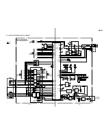
Page 17: ...2F CON OUT VOUT 46 CLV V MON 45 CLV W MON 48 CLV U CON 49 CLV V CON 50 CLV W CON 42 CLV V CON 51 24 DRV VCON VG VG CON 44 RM VCOM 2 UNREG MON 78 XREBOOT 9 MRST VDD VSS 47 CLV W MON 31 OPR LED 77 32 ADJUST OPEN CLS SW 34 XWAKE SET 8 SET KEY 23 27 HOLD SW AVLS SW 30 DBB1 29 DBB0 63 RMC DTCLK 33 XWAKE RMC B UNREG RESET IC803 D802 OPERATE TAP801 TAP803 S809 OPEN CLOSE S805 S801 S804 S803 S802 N VOL 3 ...

Page 18: ...T NORM R903 D903 C910 80 75 70 65 61 21 25 30 35 40 41 16 9 8 1 IC302 45 50 55 60 20 15 10 5 1 IC801 4 3 1 2 70 75 65 60 55 51 5 1 10 15 20 25 26 30 35 40 45 50 100 95 90 85 80 76 IC601 IC602 1 6 8 13 26 21 19 14 1 5 10 15 20 22 44 IC501 40 35 30 25 23 11 1 A B C D E F G H I 2 3 4 5 6 7 8 9 10 11 12 13 14 6 3 PRINTED WIRING BOARDS AND SCHEMATIC DIAGRAMS 6 3 1 PRINTED WIRING BOARD MAIN BOARD D351 F...

Page 19: ...NDLE MOTOR M902 SLED MOTOR 5 1 N U V W 2 3 4 6 8 7 TP558 TP555 TP502 TP503 TP504 TP564 TP565 TP559 TP557 TP560 TP563 TP501 TP567 TP552 TP551 TP803 TP562 TP553 TP801 TP561 TP814 TP569 TP615 TP602 TP911 TP952 TP528 TP523 TP809 TP610 TP607 TP613 TP608 TP609 TP606 TP603 TP604 TP605 TP601 TP612 TP611 TP524 TP505 TP566 TP568 TP518 TP570 TP573 TP575 TP577 TP512 TP576 TP574 TP522 TP572 TP527 TP507 TP514 T...

Page 20: ...numéro spécifié A B Line Power voltage is dc 1 5V and fed with regulated dc power supply from battery terminal Voltage and waveforms are dc with respect to ground under no signal conditions no mark PB Impossible to measure Voltages are taken with a VOM Input impedance 10 MΩ Voltage variations may be noted due to normal produc tion tolerances Waveforms are taken with a oscilloscope Voltage variatio...

Page 21: ...stors are in Ω and 1 4 W or less unless otherwise specified indicates tolerance C panel designation A B Line Power voltage is dc 1 5V and fed with regulated dc power supply from battery terminal Voltage is dc with respect to ground under no signal condition no mark PB Impossible to measure Voltages are taken with a VOM Input impedance 10 MΩ Voltage variations may be noted due to normal produc tion...

Page 22: ...trolytics and tantalums All resistors are in Ω and 1 4 W or less unless otherwise specified indicates tolerance A B Line Power voltage is dc 1 5V and fed with regulated dc power supply from battery terminal Voltage is dc with respect to ground under no signal condition no mark PB Impossible to measure Voltages are taken with a VOM Input impedance 10 MΩ Voltage variations may be noted due to normal...

Page 23: ...V and fed with regulated dc power supply from battery terminal Voltage and waveforms are dc with respect to ground under no signal conditions no mark PB Voltages are taken with a VOM Input impedance 10 MΩ Voltage variations may be noted due to normal produc tion tolerances Waveforms are taken with a oscilloscope Voltage variations may be noted due to normal produc tion tolerances Circled numbers r...

Page 24: ...WAVE GENERATOR OSC PWM PFM CONTROLAR PHASE COMPENSATION 3 CE 2 VDD 1 FB 5 EXT 4 GND BUFFER DRIVER IC902 XC6368B101MR IC601 UPD63731GC 9EU 21 22 23 24 25 26 27 28 29 30 2 3 5 4 6 7 8 9 10 1 11 12 13 14 15 16 17 18 19 20 31 32 33 34 35 36 37 38 39 40 51 52 53 54 55 56 57 58 59 60 61 62 63 64 65 66 67 68 69 70 41 42 43 44 45 46 47 48 49 50 71 72 73 74 75 76 77 78 79 80 81 82 83 84 85 86 87 86 89 90 1...

Page 25: ...N DECODER ROW DECODER I O BUFFER TIMING AND CONTROL 24 D2 25 D3 26 VSS 23 XCAS 22 XOE 8 A10 6 A11 5 XRAS 4 3 2 1 XWE D1 D0 VCC 7 NC 9 A0 10 A1 11 A2 12 A3 13 VCC 21 A9 20 NC 19 A8 18 A7 17 A6 16 A5 15 A4 14 VSS VREF PWM CONTROL CIRCUIT SOFT START CIRCUIT 3 NC 2 VDD 1 VOUT 5 EXT 4 VSS 2 3 5 4 6 7 8 1 V V VREF 1 NC 2 VSS 3 OUT 4 VDD IC803 S 8081ANNP EDF T2 ...

Page 26: ... RO2 61 H2VM 62 FO2 63 H2PG1 64 FI3 56 PWM24 33 34 35 36 37 38 39 40 41 42 43 44 45 46 47 48 NC NC VCC2 VCC1 H3PG1 FO3 FO3 H3VM H3VM RO3 RO3 H3PG2 CPUI CPVI CPWI COM 25 NC 26 VO 27 GNDUV 28 UO 29 VMU CPUO 31 CPVO 32 CPWO 30 18 17 ASGND 19 SGND 20 NC 21 NC 22 GNDW 23 WO 24 VMVW OE VCC2 VCC1 1 XCS SK DO DI VCC XBUSY RST GND 2 INSTRUCTION DECODE CONTROL AND CLOCK GENERATION 3 4 8 7 6 5 INSTRUCTION RE...

Page 27: ...SILVER SILVER EXCEPT US 6 4 225 566 11 FULCRUM BATTERY CASE LID BLUE BLUE 7 4 225 569 01 SHEET BLIND 8 4 218 229 17 SCREW 1 4 MI SILVER SILVER EXCEPT US 8 4 218 229 19 SCREW 1 4 MI BLUE BLUE 9 X 3378 851 1 PANEL ASSY S S UPPER SILVER SILVER EXCEPT US 9 X 3378 852 1 PANEL ASSY S L UPPER BLUE BLUE 10 4 225 587 01 SCREW MD STEP 11 X 4951 947 1 HOLDER ASSY 12 3 318 382 91 SCREW 1 7X2 5 TAPPING 13 A 33...

Page 28: ...9 4 222 208 01 GEAR SB 60 4 222 204 01 BEARING 61 4 222 203 01 SCREW LEAD 062 X 4952 387 1 SERVICE ASSY OP LCX 2E 63 4 222 205 01 SPRING RACK M901 8 835 666 01 MOTOR DC SSM 01C14A C NP SPINDLE M902 1 763 399 11 MOTOR DC SLED WITH PULLEY GEAR A A 51 52 53 M901 M902 54 55 56 57 59 61 62 57 63 60 60 58 57 57 The components identified by mark 0 or dotted line with mark 0 are critical for safety Replac...

Page 29: ... 826 11 CERAMIC CHIP 0 1uF 10 16V C552 1 107 826 11 CERAMIC CHIP 0 1uF 10 16V C553 1 107 765 11 TANTAL CHIP 3 3uF 20 16V C554 1 107 765 11 TANTAL CHIP 3 3uF 20 16V C555 1 135 238 21 TANTAL CHIP 6 8uF 20 10V C556 1 135 238 21 TANTAL CHIP 6 8uF 20 10V C557 1 164 677 11 CERAMIC CHIP 0 033uF 10 16V C558 1 164 677 11 CERAMIC CHIP 0 033uF 10 16V C559 1 164 677 11 CERAMIC CHIP 0 033uF 10 16V C561 1 164 1...

Page 30: ...60 TRANSISTOR 2SA1586 YG Q903 8 729 046 48 FET FDV303N Q904 8 729 402 16 TRANSISTOR XN4608 Q905 8 729 809 46 TRANSISTOR 2SD1935 CT6 Q906 8 729 420 44 TRANSISTOR UN5210 Q907 8 729 046 48 FET FDV303N Q908 8 729 046 48 FET FDV303N RESISTOR R101 1 216 833 11 RES CHIP 10K 5 1 16W R102 1 216 827 11 METAL CHIP 3 3K 5 1 16W R103 1 216 797 11 METAL CHIP 10 5 1 16W R104 1 216 829 11 METAL CHIP 4 7K 5 1 16W ...

Page 31: ...11 METAL CHIP 1M 5 1 16W R929 1 216 823 11 METAL CHIP 1 5K 5 1 16W NETWORK RESISTOR RB551 1 233 965 11 RES NETWORK CHIP TYPE 4 7K RB552 1 233 979 11 RES NETWORK CHIP TYPE 1M RB802 1 233 977 11 RES NETWORK CHIP TYPE 470K SWITCH S801 1 771 138 21 SWITCH KEY BOARD x S802 1 771 138 21 SWITCH KEY BOARD N S803 1 771 138 21 SWITCH KEY BOARD S804 1 771 138 21 SWITCH KEY BOARD VOL S805 1 771 138 21 SWITCH ...

Page 32: ... 42 MZ E60 Sony Corporation Personal Audio Division Company 9 927 633 11 2000A0478 1 Printed in Japan C2000 1 Published by General Engineering Dept ...

Reviews: