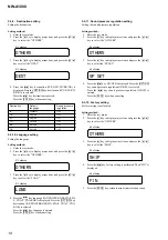
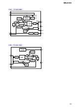
background image

NW-A1000

32

32

NW-A1000

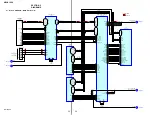
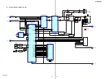
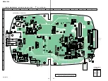
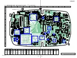
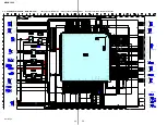
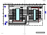
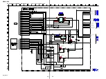
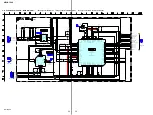
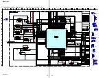
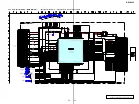
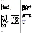
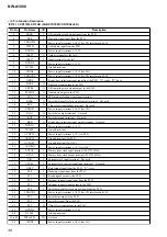
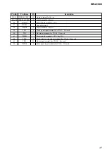
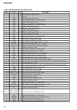
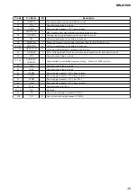
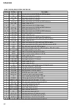
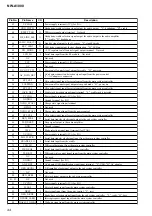
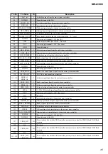
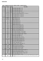
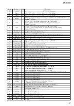
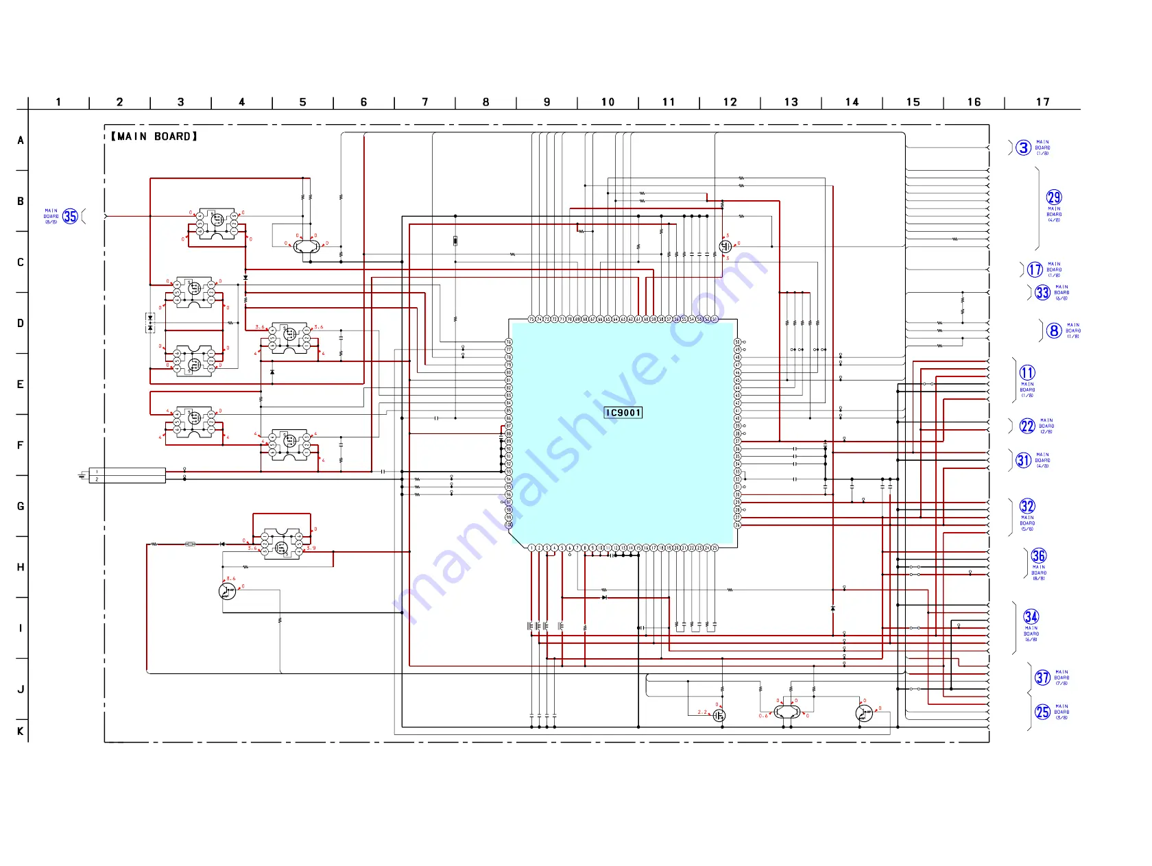
5-12. SCHEMATIC  DIAGRAM  – MAIN Board (7/8) –

 See page 36 for IC Pin Function Description.

R9007

R9008

R9009

C9038

C9003

Q9005

D9002

R9016

R9017

R9061

C9016

C9020

R9024

R9062

R9056

R9058

Q9009

R9057

Q9011

R9001

D9006

Q9013

C9001

R9003

D9001

R9004

R9002

CN9001

R9005

C9002

C9039

D9005

Q9006

R9059

Q9008

TH9002

TH9001

R9042

R9033

R9043

R9044

R9066

R9040

R9034

R9035

R9036

R9039

R9047

C9022

C9023

C9024

C9025

C9033

C9034

R9013

D9003

R9015

C9010

R9018

R9020

R9022

C9011

C9014

C9017

C9004

C9006

C9008

C9040

R9060

R9021

R9011

R9012

Z9004

Z9001

C9019

R9053

R9054

R9050

R9051

R9067

R9041

Q9010

FB9001

FB9002

R9006

R9048

R9049

D9004

Z9002

C9028

C9037

C9030

R9069

TP9028

Q9012

Q9007

IC9001

µ

PD68855F9-

Y03-BA2-E2-A

L9001

L9002

2.2 

µ

H

3.3 

µ

H

4.7 

µ

H

4.7 

µ

H

L9003

L9004

R9010

R9063

Q9003

C9012

Q9014

TP9018

Q9002

Q9001

TP9023

TP9031

TP9027

TP9026

TP9024

Z9005

Z9003

SP9023

SP9007

TP9008

TP9009

TP9010

TP9011

TP9012

TP9013

TP9014

TP9015

TP9016

SP9020

SP9019

SP9026

SP9025

TP9005

SP9003

SP9004

SP9005

SP9006

SP9021

TP9032

TP9001

TP9002

TP9025

TP9029

TP9030

470k

470k

470k

22

0.1

MTM26130L

MA22D39

470k

470k

0

1200p

1200p

0

1M

470k

100k

NP0A50100AS0

47k

MTM26130L

0.33

MAS3132EOLSO

MTM26130L

1000p

1k

MA22D2800LS0

4.7k

0.33

2P

100

0.022

0.1

MA22D39

MTM26130L

1M

DTC114YMT2L

470k

100k

470k

470k

0

0

150k

100k

100k

100k

0

1

1

2.2

1

1

1

0

RB521S-30-TE61

100k

22

10k

10k

10k

1500p

1500p

1500p

22

22

22

22

470k

0

470k

470k

10

0

0

3.3k

470

470k

470k

2SK354700LS0

0

0

4.7k

6.8k

0

RB521S-30-TE61

1

0.01

1

100k

(3.3V)

DTC114YMT2L

NP0A50100AS0

10k

470

UPA1919

6800p

2SJ067400LS0

(VSTBY)

UPA1919

UPA1919

(1.3V)

(3.0V)

(1.10V)

(1.8V)

(5.0V)

SUSPEND

DCIN

VBUS

DC_OUT

DC_OUT_CTL

VSTBY

3.0V

3.3V

GND

CHG_LED

3.3V_HDD

3.3V_A

5.0V

VB

GND_HDD

GND_A

RST

SET_KEY(K2)

RMCKEY(K1)

PWR_SLEEP

XRST

XVBUS_LIM

AD_BATT

BAT_MON_CTL

DCIN_DET

CHG_STAT1

AD_RMCKEY(K1)

EX_MULTI_SCK

EX_MULTI_SO

PWR_STRB

MULTI_SI

PWR_FFCLR

3.3V

3.0V

GND

AD_GND

VB

3.3V

GND

3.3V

GND

GND

3.0V

GND

3.0V

GND

XCHG_STAT2

1.10V

1.8V

1.3V

1.8V

1.10V

1.8V

GND_A

R

S

T

G

N

D

_

S

W

S

O

X

C

H

G

_

S

T

A

T

2

D

C

IN

_

D

E

T

B

A

T

_

M

O

N

_

C

T

L

A

D

_

B

A

TT

X

C

H

G

_

S

T

A

T

1

XVBUS_LIM

PWR_SLEEP

PWR_FFCLR

RMCKEY(K1)

WAKE1

SET_KEY(K2)

XCHG_STAT1

CHG_STAT1

RST

SET_KEY(K2)

PWR_SLEEP

XRST

XVBUS_LIM

AD_BATT

BAT_MON_CTL

DCIN_DET

CHG_STAT1

EX_MULTI_SCK

EX_MULTI_SO

XCS

SO

GND_SW

D

C

IN

S

U

S

P

E

N

D

SUSPEND

D

C

O

U

T

D

C

_

O

U

T

_

C

T

L

DC_OUT_CTL

PWR_FFCLR

DCIN

DCOUT

WAKE1

RMCKEY(K1)

X

R

S

T

XCHG_STAT2

X

C

S

E

X

_

M

U

L

T

I_

S

C

K

E

X

_

M

U

L

T

I_

S

O

NC

NC

NC

TEST4

TEST3

TEST2

TEST1

DISGND

BGGND

GND

GND

GND

VCC

VCC

CHGREG

GATE3

GATE2

GATE1

RMONI22

RMONI21

RMONI12

RMONI11

RST

GPIO1

GPIO0

SO

S

I

SCK

CS

LO

GIC

_H

TS

XCHG

_STAT2

XCHG

_STAT1

VBUSS

USPEM

D

XVBU

S_D

ET

XD

CIN_DET

B

ATTM

O

N_CN

T

BATTM

ON

VBATT

V

BUS_LIM

VBUSIN

DCIN

_M

ON

I

SEL2

SEL1

SEQSEL

CRST3

CRS

T2

CRST

1

XRST3

STBY

XRST1

XRST2

CLR

WAKE6

WAKE5

WAKE4

WAKE3

WAKE2

WAKE1

WAKE0

VSUS2

VSUS1

VSTBY

VREF

BG3

BG2

BG1(VDD)

BG1

LDO3OUT

LDO2OUT

LDO1OUT

LDO3IN

LDO2IN

LDO1IN

A2OUT

A3IN

A3OUT

A2IN

A1OUT

A1IN

FB4

FB3

FB2

FB1

GNDVO3

GND

VO3

GNDVO2

GND

VO1

VCCVO3

VCCVO

3

VC

CV

O2

VC

CV

O1

DCD

C4EN

VO4-2

VO

4

VO

3

VO3

VO

2

VO1

BATT

BATT

G

ND_

SW

-1-2

CHARGE

S

-1-2

(7/8)

CSP(Chip Size Package)

CONTROL

CHARGE

SWITCH

S

CHARGE

DETECT

CHARGE CURRENT

SWITCH

POWER CONTROL,CHARGE CONTROL

Q9005,9009

B+ SWITCH

B+ SWITCH

B+ SWITCH

Q9011,9013

B+ SWITCH

B+ SWITCH

Q9006,9008

B+ SWITCH

BATTERY

LITHIUM ION

3.7V 600mAh

CTO19

(Page 26)

(Page 29)

(Page 26)

(Page 31)

(Page 26)

(Page 26)

(Page 27)

(Page 29)

(Page 30)

(Page 33)

(Page 31)

(Page 33)

(Page 28)

(Page 33)

Summary of Contents for NW-A1000

Page 1: ...ompression technology MPEG 1 Audio Layer 3 MP3 Adaptive Transform Acoustic Coding ATRAC Maximum recordable number of track and time Approx Bit rate Tracks Time 48 kbps 4 000 266 hours 40 minutes 64 kbps 3 000 200 hours 96 kbps 2 000 133 hours 20 minutes 128 kbps 1 500 100 hours 132 kbps 1 500 100 hours 160 kbps 1 200 80 hours 192 kbps 1 000 66 hours 40 minutes 256 kbps 750 50 hours 320 kbps 600 40...

Page 2: ...RICAL PARTS LIST 50 Notes on chip component replacement Never reuse a disconnected chip component Notice that the minus side of a tantalum capacitor may be damaged by heat Flexible Circuit Board Repairing Keep the temperature of the soldering iron around 270 C during repairing Do not touch the soldering iron on the same conductor of the circuit board within 3 times Be careful not to apply force on...

Page 3: ... away if the heated tip is applied for too long so be careful Strong viscosity Unleaded solder is more viscous sticky less prone to flow than ordinary solder so use caution not to let solder bridges occur such as on IC pins etc Usable with ordinary solder It is best to use only unleaded solder but unleaded solder may also be added to ordinary solder NOTES ON REPLACEMENT OF CSP CHIP SIZE PACKAGE IC...

Page 4: ...4 NW A1000 SECTION 2 GENERAL This section is extracted from instruction manual ...

Page 5: ...rap 2 adhesive sheet strap 4 Remove the cabinet lower in the direction of the arrow Note Execute the confirmation and the inspection of the correct repair of all parts after it repairs And install ornament strap and adhesive sheet strap after confirming the repair ended completely 3 2 CASE LOWER Page 5 3 3 LITHIUM ION BATTERY Page 6 3 4 CABINET INNER Page 6 3 5 EL BLOCK SUB ASSY Page 7 3 6 MAIN BO...

Page 6: ...lectrostatic CU hole 2 two claws sheet cabinet middle AEP UK Korean 2 two claws 3 cabinet upper 5 sheet cabinet US Canadian Australian sheet ESD AEP UK Korean 4 cabinet inner sub assy button side cabinet upper ditch 1 sheet HD tweezers 1 sheet HD 2 sheet HD 3 1 Hang claw and ditch of cabinet upper completely Note Do not damage it when you peel off sheet ESD from sheet cabinet middle tweezers claw ...

Page 7: ...nstallation of EL block sub assy adjust the position of two bosses and slit or hole Note On installation of sheet electrostatic CU pass the sheet electrostatic CU through this ditch 6 MAIN board 3 insulator CF1 3 insulator CF1 5 HDD unit 4 connector unit connector unit HDD unit HITACH or Seagate is printed 1 connector CN5001 2 knob VOL S8301 Note On installation of MAIN board adjust the position o...

Page 8: ...NW A1000 8 3 7 POSITION OF FERRITE CORE 2cm A cable is rolled onece clamp filter ferrite core Part No 1 500 386 11 AC POWER CORD Ver 1 2 ...

Page 9: ... 3 V 5 0 V are starting is checked Checking method 1 Enter the test mode 2 Press the B key to display major item and press the v V key to select the POWER EL display POWER 3 Press the B key to display minor item and press the v V key to select the V CHK EL display V CHK 4 Press the u key START is displayed and all power supply lines are started EL display START In this state the power supply volta...

Page 10: ...read state is completed EL display READ r FIN 6 Press the BACK key return to minor item selection screen 5 1 3 Consumption current write state check This mode is used in case consumption current write state in the state where the hard disk drive has booted is checked Checking method 1 Enter the test mode 2 Press the B key to display major item and press the v V key to select the POWER EL display P...

Page 11: ...the v V key to select the SN EL display SN 4 Press the u key START is displayed and Infinity Zero VOLUME 27 audio signal is outputted EL display START 5 Press the BACK key return to minor item selection screen 5 2 3 Frequency characteristic check 20 Hz 20 kHz 100 Hz 10 kHz 0 dBs L ch R ch VOLUME 21 audio signal is outputted Checking method 1 Enter the test mode 2 Press the B key to display major i...

Page 12: ...ay major item and press the v V key to select the AUDIO EL display AUDIO 3 Press the B key to display minor item and press the v V key to select the MAXOUT EL display MAXOUT 4 Press the u key START is displayed and 1kHz 0dBs L ch R ch VOLUME 30 audio signal is outputted In this state each time OPTION key is pressed AVLS ON OFF switch is performed EL display START 5 Press the BACK key return to min...

Page 13: ... displayed and 10 kHz 20 dBs L ch R ch VOLUME 30 audio signal is outputted EQ LEVEL MAX MIN OFF switch is performed EL display START 20 Press the BACK key return to minor item selection screen 5 2 7 BEEP check BEEP sound is outputted Checking method 1 Enter the test mode 2 Press the B key to display major item and press the v V key to select the AUDIO EL display AUDIO 3 Press the B key to display ...

Page 14: ...y Z axis direction is displayed Press the BACK key return to minor item selection screens EL display Z A D value hexadecimal 7 Press the BACK key return to minor item selection screen 5 3 2 Clock check Clock operation is checked Checking method 1 Enter the test mode 2 Press the B key to display major item and press the v V key to select the OTHERS EL display OTHERS 3 Press the B key to display min...

Page 15: ... the u key EL all segments turned off 8 Press the BACK key return to minor item selection screen 9 Press the v V key to select the OEL3 EL display OEL3 10 Press the u key monochrome lattice is displayed on the EL 11 Press the BACK key return to minor item selection screen 12 Press the v V key to select the OEL4 EL display OEL4 13 Press the u key monochrome lattice reverse version of step 10 is dis...

Page 16: ...set and the sensitivity of each axis are displayed by pressing the u key when normally completing in order of X Y and Z EL display offset sensitivity 12 Press the BACK key return to minor item selection screen 5 3 6 G sensor adjustment check This mode checks that G sensor adjustment is performed or not performed Checking method 1 Enter the test mode 2 Press the B key to display major item and pres...

Page 17: ...in the check of hard disk drive Checking method 1 Enter the test mode 2 Press the B key to display major item and press the v V key to select the OTHERS EL display OTHERS 3 Press the B key to display minor item and press the v V key to select the HDDCHK EL display HDDCHK 4 Press the u key READY is displayed EL display READY 5 Press the u key check of hard disk drive is started When the display cha...

Page 18: ... ENG FRE GER ITA SPA S_CNA T_CNA KOR is displayed Press the OPTION key destination JAP ENG FRE GER ITA SPA S_CNA T_CNA KOR is selected Press the u key language is entered Press the BACK key when canceling 5 3 11 Sound pressure regulation setting Setting the sound pressure regulation Setting method 1 Enter the test mode 2 Press the B key to display major item and press the v V key to select the OTH...

Page 19: ...s displayed automatically EL display START r OK 5 Press the BACK key return to minor item selection screen 5 3 14 Hard disk drive serial No display Serial No of hard disk drive is displayed Checking method 1 Enter the test mode 2 Press the B key to display major item and press the v V key to select the OTHERS EL display OTHERS 3 Press the B key to display minor item and press the v V key to select...

Page 20: ...54 XINT_DENDE 84 DATA_READY 121 XINT_DENDE 124 DENDE_SREQ 53 WAKEUP_DENDE 52 DENDE_SS 98 TSB_RW 66 DENDE_SERQ 87 WAKEUP_DENDE 88 DENDE_SS 120 TSB_RW 74 TSB_SO 72 SD RAM IC7001 USB CONTROLLER IC5001 MAIN SYSTEM CONTROLLER IC6005 1 2 PLD IC8001 1 3 100 XO 99 XI X5001 12MHz 35 CROUT 34 CRIN X6001 22 5792MHz 2 4 5 7 8 10 11 13 42 44 45 47 48 50 51 53 D16 D31 D24 D31 D16 D31 FRES_D24 FRES_D31 FRES_A1 F...

Page 21: ...4 BCK 2 LRCK 1 DEN_SERQ 94 WAKEUP_DEN 93 XRESET_DEN 96 PF2 36 PF0 34 NRST 30 XTAL 29 EXTAL X3101 22 5792MHz 33 DEN_SI0 92 DEN_SCK0 65 DEN_SCS0 105 PC2 41 PC0 38 PC3 42 DEN_XRDE 86 XRDE 12 DEN_DATA_RDY 104 PF1 35 XINT_DEN 102 PF3 37 DEN_PCMD0 103 DEN_BCK0 101 DEN_LRCK0 106 PCMD0 15 BCK0 13 LRCK0 14 DEN_SO0 73 PC1 40 SUB SYSTEM CONTROLLER IC3101 CRADLE ON OFF SWITCH Q1002 2002 AUDIO SIGNAL PATH HEAD...

Page 22: ...E3 85 GPIO0 76 GATE1 83 VBUSIN 1 10V 59 RMONI21 81 VCC 88 VCC VCCVO1 VCCVO2 VCCVO3 VCCVO4 87 B SWITCH Q9001 10 11 9 8 TO CHARGE CRADLE OR DOG SPEAKER 2 5V 4 5V 7 DCOUT B SWITCH Q9011 9013 B SWITCH Q9006 9008 B SWITCH Q9005 9009 DC DC CONVERTER IC8302 DCIN_MON 58 RMONI11 79 RMONI12 80 VBUS A RMCKEY G D9002 B SWITCH Q9002 D8305 LED VCC VB DC DC CONVERTER IC8301 D8303 D9003 17V FOR EL MODULE VO1 1 XC...

Page 23: ...e are indicated Parts face side Parts on the parts face side seen from Component Side the parts face are indicated surface The voltage and waveform of CSP chip size package cannot be measured because its lead layout is different from that of conventional IC Waveforms MAIN board is multi layer printed board However the patterns of intermediate layer have not been included in diagram Lead Layouts Re...

Page 24: ...6039 C8002 C8003 C8001 C8008 C8009 C8017 R5026 R5034 R5035 R5024 R5021 R5022 R5028 R5025 R8011 R8008 R8013 R8012 F3001 CN9001 FB7001 S8302 S901 L9004 CN9201 MAIN BOARD COMPONENT SIDE 1 868 436 11 11 A B C D E F G 1 2 3 4 5 6 7 8 9 10 11 TP6003 TP6026 TP6004 TP8077 TP8058 TP1002 TP1001 TP9005 TP9030 TP4201 TP4202 TP4203 TP302 TP8303 TP303 TP304 TP305 TP101 TP9025 TP201 TP306 TP9201 TP9011 TP9010 TP...

Page 25: ... 2B 2C 2 24 1 25 EL MODULE 1B 2E 2B 1C 1E 2C 2C 2E 1C 2B 1E 1B 28 33 36 39 42 45 48 51 54 30 32 35 38 40 44 47 50 53 29 31 34 37 41 43 46 49 52 26 23 20 17 14 12 9 6 3 25 24 21 18 15 11 8 5 2 27 22 19 16 13 10 7 4 1 22 18 15 11 7 3 21 17 14 12 8 4 23 19 16 10 6 2 24 20 13 9 5 1 25 29 33 40 44 48 26 30 34 39 43 47 28 32 36 37 41 45 27 31 35 38 42 46 1 3 5 4 2 4 64 1 7 9 11 14 15 16 5 6 63 3 8 10 12...

Page 26: ..._D31 FRES_D16 FRES_XWE FRES_XCAS FRES_XRAS FRES_XCS FRES_XLDQM FRES_XUDQM FRES_CKE FRES_CLK FRES_CLK FRES_CKE FRES_XUDQM FRES_XLDQM FRES_XCS FRES_XRAS FRES_XCAS FRES_XWE SDATAO2 LRCK2 SCLK2 XRESET_USB DENDE_SS HOLD_KEY XINT_DENDE RDY_XBUSY SCLK3 LRCK3 SDATAI3 FS256 TSB_RW SDATAO1 LRCK1 SCLK1 SPI_CS0 SPI_CS1 MULTI_SO MULTI_SCK MULTI_SI FRES_XCS1 DATA_READY DENDE_SREQ WAKEUP_DENDE SPI_CS2 XRESET_LCD...

Page 27: ...A16 FRES_A15 FRES_A14 FRES_A13 FRES_A12 FRES_A11 FRES_A10 FRES_A09 FRES_A20 FRES_A21 FRES_A19 FRES_A18 FRES_A8 FRES_A7 FRES_A6 FRES_A5 FRES_A4 FRES_A3 FRES_A2 FRES_A17 FRES_D31 FRES_D30 FRES_D29 FRES_D28 FRES_D27 FRES_D26 FRES_D25 FRES_D24 FRES_A21 FRES_A19 FRES_A18 FRES_A9 FRES_A10 FRES_A11 FRES_A12 FRES_D16 FRES_D17 FRES_D18 FRES_D19 FRES_D20 FRES_D21 FRES_D22 FRES_D23 FRES_A22 FRES_A23 FRES_A20...

Page 28: ...008S0 100k 1M 510k 10p 1 0 4 7 1M 680 680 1k 1 5k 3 3k 100k 100k 4 7 4 7 100k 470 MAS3132E0LSO 47k 100 6 3V 30k 100 47k 100 6 3V 30k 100 2SC5658T2LQ R 4 7 1M MA2S728 K8 SO 0 1 1k 11P TPS61041 2SC5658T2LQ R 470k 4 7 4 7 100 CL 270TLY C TS F VB 3 0V GND KEY_LED1 KEY_LED2 LCD_XCS XRESET_LCD LCD_DC FRES_RXW FRES_XOE EX_MULTI_SCK EX_MULTI_SO AD_KEY1 AD_KEY2 SET_KEY K2 RST VSTBY EL_PWR HOLD_KEY AD_KEY2 ...

Page 29: ...RES_A3 FRES_D27 FRES_D26 FRES_D25 FRES_D24 TSB DC_OUT_CTL SUSPEND SCLK1 LRCK1 MULTI_SCK EX_MULTI_SCK SDATAO1 MULTI_SO XINT_DENDE DATA_READY LRCK3 SCLK3 SDATAI3 WAKEUP_DENDE DENDE_SREQ CRADLE_SCK CRADLE_SI CRADLE_SO TSB_RW AF_DCIN_DET KEY_LED2 KEY_LED1 HP_MUTE HP_CRD_SEL HP_LINE_SEL XGSEN_PWR_CTL PWR_SLEEP PWR_FFCLR BAT_MON_CTL XVBUS_LIM XHDD_PWR_CTL FS256 DENDE_SS SCLK2 AF_XRST XINT_DEN DEN_DATA_R...

Page 30: ... CXR710160 215GH 0 0 MA2S728 K8 SO 0 1 0 1 2p 22 220k XRESET_DEN DEN_SO0 XINT_DEN DEN_DATA_RDY DEN_PCMD0 DEN_LRCK0 DEN_BCK0 VB 3 0V MULTI_SO EX_MULTI_SCK RTC_CE GND AD_GSEN_X AD_GSEN_Y AD_GSEN_Z XGSEN_PWR_CTL DENDE_IN DEN_XRDE DEN_SCS0 1 3V 1 8V WAKEUP_DEN DEN_SREQ DEN_SCKO DEN_SIO DEN_PCMDI DEN_BCKI DEN_LRCKI XGSEN_PWR_CTL XGSEN_PWR_CTL DEN_SCSO DEN_SCSO DEN_SO0 XRESET_DEN XRESET_DEN XINT_DEN XIN...

Page 31: ...6 3V 47 6 3V 47 6 3V 22 4V 47 6 3V 0 01 1 47 6 3V 10 22 4V 22 0 01 10k 0 01 10k 47k 0 47 10k 150k 0 1 6 3V 10 6 3V 1 10 6 3V 1 0 1 15k 0 15k 33k 1 0 0 1 PCM1772 2200p 2200p 1 0 0 0 0 0 25A 125V 680k XP4213 TXE 2SC5585TL AN17020A VB 0 XC6219B282DR UNR31A300LS0 4 7k 4 7k 33k 33k 220k 0 470p 470p 2 2 6 3V 220 2 5V 22 6 3V 220 2 5V UNR31A300LS0 1k MA133 TX EDZTE616 8B EDZTE616 8B MAZWO68HOLSO MAZWO68H...

Page 32: ...PA1919 1 3V 3 0V 1 10V 1 8V 5 0V SUSPEND DCIN VBUS DC_OUT DC_OUT_CTL VSTBY 3 0V 3 3V GND CHG_LED 3 3V_HDD 3 3V_A 5 0V VB GND_HDD GND_A RST SET_KEY K2 RMCKEY K1 PWR_SLEEP XRST XVBUS_LIM AD_BATT BAT_MON_CTL DCIN_DET CHG_STAT1 AD_RMCKEY K1 EX_MULTI_SCK EX_MULTI_SO PWR_STRB MULTI_SI PWR_FFCLR 3 3V 3 0V GND AD_GND VB 3 3V GND 3 3V GND GND 3 0V GND 3 0V GND XCHG_STAT2 1 10V 1 8V 1 3V 1 8V 1 10V 1 8V GND...

Page 33: ... H_D2 H_D3 H_D4 H_D5 H_D6 H_D7 H_D8 H_D9 H_D10 H_D11 H_D12 H_D13 H_D14 H_D15 HDMARQ XHIOW XHIOR XHIORDY FRES_A1 FRES_A2 FRES_A3 FRES_A4 FRES_A5 FRES_A6 FRES_A7 FRES_A8 IDE_DIOR IDE_DIOW XINT_USB FRES_D24 FRES_D25 FRES_D26 FRES_D27 FRES_D28 FRES_D29 FRES_D30 FRES_D31 IDE_DIOR IDE_DIOW XINT_USB CRADLE_CS CRADLE_CS CRADLE_SI CRADLE_SI CHG_LED CHG_LED CRADLE_SO CRADLE_SO RMCKEY K1 RMCKEY K1 CRADLE_SCK...

Page 34: ...VCC1 VCOM POWER SUPPLY 2 1 4 3 GND CH1 IN VCC 1HV CH2 IN 15 16 13 14 MUTING CTRL CH1 SENS BEEP 6 5 8 7 VCC1 RF VCC2 VCC 2HV BEEP LINE AMP HEADPHONE AMP MUTING LINE AMP HEADPHONE AMP 12 11 9 10 CH1 OUT PGND CH2 SENS CH2 OUT REF1 VREF REF2 HP LINE SWITCH IC4101 R2061K01 E2 SIO 1 SCLK 2 7 OSCIN VSB 4 VCC 5 VDD 6 CE 12 CIN 10 VSS 11 LEVEL SHIFTER DELAY REAL TIME CLOCK VDCC 3 VOLTAGE DETECTOR BATTERY V...

Page 35: ... MAX ON TIME GATE DRIVER GATE DRIVER DIGITAL INTERFACE 6 BIT D A CONVERTER S R ERROR COMPARATOR VREF CURRENT LIMIT SOFT START CTRL INPUT SWITCH MAIN SWITCH IC8302 TPS61041DBVR 1 SW FB 3 GND 2 5 VIN 4 EN RS LATCH LOGIC UNDER VOLTAGE LOCKOUT BIAS SUPPLY 400 ns MIN OFF TIME 6 µs MAX ON TIME GATE DRIVER S R ERROR COMPARATOR VREF CURRENT LIMIT SOFT START ...

Page 36: ...I O 20 KDO O Serial data output terminal Not used 21 KDI I Serial data input terminal Not used 22 KRB O Ready busy selection signal output terminal Not used 23 DVDD1 Power supply terminal 1 3V 24 DVSS3 Ground terminal 25 AVDPLL Power supply terminal 3V for PLL 26 AVSPLL Ground terminal for PLL 27 AVSOSC Ground terminal for OSC 28 AVDMO Power supply terminal 3V for OSC 29 EXTAL I Main system clock ...

Page 37: ...3V 57 DVSS1 Ground terminal 58 TEST0 I Input terminal for the test 59 TCK I Clock signal input terminal for JTAG Not used 60 TDI I Data input terminal for JTAG Not used 61 VDIO3 Power supply terminal 1 8V for I O 62 TMS I Mode selection signal input terminal for JTAG Not used 63 TDO O Data output terminal for JTAG Not used 64 NTRST I Reset signal input terminal for JTAG Not used ...

Page 38: ...ite signal input from the main system controller 31 XINT O Interrupt request signal output to the main system controller 32 to 35 CD0 to CD3 I O Two way data bus with the main system controller SD RAM NOR flash memory and PLD 36 VSS Ground terminal logic system 37 to 40 CD4 to CD7 I O Two way data bus with the main system controller SD RAM NOR flash memory and PLD 41 VDD Power supply terminal 3 3V...

Page 39: ...isk drive unit 83 84 HCS0 HCS1 O Chip select signal output to the hard disk drive unit 85 XHDASP I Drive valid signal and slave drive detection signal input from the hard disk drive unit 86 VSS Ground terminal logic system 87 88 CLKSEL0 CLKSEL1 I Input terminal for oscillation frequency setting Fixed at 12 MHz in this set 89 VSS Ground terminal logic system 90 XVSS Ground terminal logic system 91 ...

Page 40: ...erminal 3V for OSC 34 CRIN I Main system clock input terminal 22 5792 MHz 35 CROUT O Main system clock output terminal 22 5792 MHz 36 OSC_PAD_GND Ground terminal for OSC 37 PLL_CORE1_VDD Power supply terminal 1 1V for PLL 38 CORE_VDD Power supply terminal 1 1V for core 39 CORE_GND Ground terminal for core 40 PLL_CORE1_GND Ground terminal for PLL 41 OE O Read signal output to the NOR flash memory P...

Page 41: ...ry L busy H ready 83 XBATT_DET I Battery insert detection signal input terminal Not used 84 XINT_DENDE I Interrupt request signal input from the PLD 85 USB _IF_EN O USB interface enable signal output terminal Not used 86 XINT_USB I Interrupt request signal input from the USB controller 87 XINT_HDD I Interrupt request signal input from the hard disk drive Not used 88 GSEN_SEL2 O G sensor axis selec...

Page 42: ... signal output to the SD RAM 126 BCLK O Clock signal output to the SD RAM 127 128 DATA31 DATA30 I O Two way data bus with the USB controller SD RAM NOR flash memory and PLD 129 PAD_GND Ground terminal for I O 130 to 134 DATA29 to DATA25 I O Two way data bus with the USB controller SD RAM NOR flash memory and PLD 135 PAD_VDD Power supply terminal 3V for I O 136 DATA24 I O Two way data bus with the ...

Page 43: ... 19 FRES_D30 I O Two way data bus with the USB controller main system controller SD RAM and NOR flash memory 20 RTC_CE O Chip enable signal output to the real time clock H active 21 FRES_D31 I O Two way data bus with the USB controller main system controller SD RAM and NOR flash memory 22 PWR_STRB O Chip select signal output to the power control H active 23 PWR_SLEEP O Standby signal output to the...

Page 44: ...tate signal input terminal 62 GPIO5 I Not used 63 XCHG_STAT2 I Charge state signal input from the power control 64 SPI_CS0 I Chip select signal input for serial control from the main system controller 65 DEN_SCK0 O Serial data transfer clock signal output to the sub system controller 66 PLD_BEEP O Beep signal output to the audio amplifier 67 GND Ground terminal 68 TMS I Mode selection signal input...

Page 45: ...W I Read write control signal input from the main system controller 110 IIS_CLR_IN I IIS CLR control signal input terminal 111 112 FRES_A3 FRES_A2 I Address signal input from the main system controller 113 FRES_XOE I Read signal input from the main system controller 114 FRES_A1 I Address signal input from the main system controller 115 FRES_XCS1 I Chip select signal input from the main system cont...

Page 46: ...nal for VO3 26 LDO1IN I Power supply input terminal 1 8V for LDO1 27 LDO2IN I Power supply input terminal 3 3V for LDO2 28 LDO3IN I Power supply input terminal for LDO3 Not used 29 LDO1 O Power supply output terminal 1 3V 30 LDO2 O Power supply output terminal 3V 31 LDO3 O Power supply output terminal Not used 32 BG1 O Power supply BG1 output terminal 2 8V 33 BG1 VDD I Power supply BG1 input termi...

Page 47: ...ode H USB suspend mode 67 XCHG_STAT1 O Charging flag output terminal L active 68 XCHG_STAT2 O Charge completion flag output terminal L active 69 TS I Temperature sensor input terminal 70 LOGIC_H I Power supply input terminal 3V for logic H 71 CS I Chip select signal input from the PLD H active 72 SCK I Serial data transfer clock signal input from the PLD 73 SI I Serial data input from the PLD 74 S...

Page 48: ...025 1 CABINET INNER V SUB ASSY for VIOLET 1 X 2109 026 1 CABINET INNER B SUB ASSY for BLACK 2 2 662 670 02 SHEET CABINET US CND AUS 2 2 668 889 01 SHEET ESD AEP UK SP KR 3 2 651 522 01 CABINET UPPER VIOLET 3 2 651 522 11 CABINET UPPER PINK 3 2 651 522 21 CABINET UPPER BLUE 3 2 651 522 31 CABINET UPPER SILVER 3 2 651 522 41 CABINET UPPER BLACK 3 2 651 522 51 CABINET UPPER GOLD 4 2 662 680 01 GASKET...

Page 49: ...16 1 BUTTON LINK L SUB ASSY BLUE 61 X 2108 217 1 BUTTON LINK S SUB ASSY SILVER 61 X 2108 228 1 BUTTON LINK B SUB ASSY BLACK 61 X 2108 229 1 BUTTON LINK N SUB ASSY GOLD 62 2 651 527 01 BUTTON HOLD for BLUE SILVER VIOLET PINK BLACK 62 2 651 527 11 BUTTON HOLD for GOLD 63 2 652 123 01 KNOB VOL for BLUE SILVER VIOLET PINK BLACK 63 2 652 123 11 KNOB VOL for GOLD 64 1 479 526 12 HDD UNIT 6GB 65 1 479 53...

Page 50: ...CHIP 1uF 20 16V C3035 1 125 891 11 CERAMIC CHIP 0 47uF 10 10V C3038 1 100 415 11 CERAMIC CHIP 0 47uF 10 6 3V C3101 1 100 504 11 CERAMIC CHIP 0 1uF 20 6 3V C3102 1 100 506 11 CERAMIC CHIP 1uF 20 6 3V C3103 1 128 617 11 CERAMIC CHIP 100PF 5 25V C3104 1 100 504 11 CERAMIC CHIP 0 1uF 20 6 3V C3105 1 100 506 11 CERAMIC CHIP 1uF 20 6 3V C3106 1 100 504 11 CERAMIC CHIP 0 1uF 20 6 3V C3107 1 100 504 11 CE...

Page 51: ... C6052 1 100 504 11 CERAMIC CHIP 0 1uF 20 6 3V C6053 1 100 504 11 CERAMIC CHIP 0 1uF 20 6 3V C6054 1 128 626 11 CERAMIC CHIP 680PF 10 16V C6055 1 100 504 11 CERAMIC CHIP 0 1uF 20 6 3V C6056 1 100 506 11 CERAMIC CHIP 1uF 20 6 3V C6057 1 128 617 11 CERAMIC CHIP 100PF 5 25V C6058 1 128 617 11 CERAMIC CHIP 100PF 5 25V C6059 1 128 617 11 CERAMIC CHIP 100PF 5 25V C6060 1 128 617 11 CERAMIC CHIP 100PF 5 ...

Page 52: ...301 8 719 046 85 DIODE MA2S728 D8302 8 719 046 85 DIODE MA2S728 D8303 6 500 813 01 DIODE MA2SD32008S0 D8304 6 500 840 01 LED CL 270TLY C TS F LINK D8305 6 500 813 01 DIODE MA2SD32008S0 D8306 6 500 314 01 DIODE DAN222MT2L D9001 6 500 483 01 DIODE MA22D2800LS0 D9002 6 501 286 01 DIODE MA22D3900LS0 D9003 8 719 071 34 DIODE RB521S 30 TE61 D9004 8 719 071 34 DIODE RB521S 30 TE61 D9005 6 501 286 01 DIOD...

Page 53: ...8 1 218 961 11 RES CHIP 4 7K 5 1 16W R1009 1 218 977 11 RES CHIP 100K 5 1 16W R1020 1 218 933 11 RES CHIP 22 5 1 16W R1023 1 218 965 11 RES CHIP 10K 5 1 16W R1024 1 218 957 11 RES CHIP 2 2K 5 1 16W R2002 1 218 990 11 SHORT CHIP 0 R2004 1 208 711 11 METAL CHIP 15K 0 5 1 16W R2005 1 208 923 11 METAL CHIP 33K 0 5 1 16W R2008 1 218 961 11 RES CHIP 4 7K 5 1 16W R2009 1 218 977 11 RES CHIP 100K 5 1 16W ...

Page 54: ...11 RES CHIP 100K 5 1 16W R6007 1 218 990 11 SHORT CHIP 0 R6008 1 218 990 11 SHORT CHIP 0 R6009 1 218 965 11 RES CHIP 10K 5 1 16W R6014 1 218 990 11 SHORT CHIP 0 R6015 1 218 990 11 SHORT CHIP 0 R6016 1 218 989 11 RES CHIP 1M 5 1 16W R6017 1 218 990 11 SHORT CHIP 0 R6018 1 218 990 11 SHORT CHIP 0 R6019 1 218 990 11 SHORT CHIP 0 R6020 1 218 990 11 SHORT CHIP 0 R6022 1 218 965 11 RES CHIP 10K 5 1 16W ...

Page 55: ...S CHIP 30K 5 1 16W R8348 1 218 973 11 RES CHIP 47K 5 1 16W R8349 1 218 823 11 METAL CHIP 100 0 5 1 10W R8350 1 216 864 11 SHORT CHIP 0 R8351 1 218 977 11 RES CHIP 100K 5 1 16W R8352 1 218 977 11 RES CHIP 100K 5 1 16W R9001 1 219 797 11 METAL CHIP 0 33 1 1 4W R9002 1 219 797 11 METAL CHIP 0 33 1 1 4W R9003 1 218 953 11 RES CHIP 1K 5 1 16W R9004 1 218 961 11 RES CHIP 4 7K 5 1 16W R9005 1 218 941 11 ...

Page 56: ...CORD 0 1 555 074 81 CORD POWER AC POWER CORD AUS 0 1 823 935 81 CORD AC POWER AC POWER CORD UK 0 1 823 947 61 POWER SUPPLY CORD AC POWER CORD KR 0 1 824 910 41 CORD POWER AC POWER CORD AEP SP 0 1 829 810 51 CORD POWER AC POWER CORD US CND 1 831 406 11 CORD WITH PLUG Headphone extension cord 2 657 722 13 GUIDE QUICK START ENGLISH EXCEPT KR 2 657 722 23 GUIDE QUICK START FRENCH CND AEP SP 2 657 722 ...

Page 57: ...57 NW A1000 MEMO ...

Page 58: ...ump to the next revised page Ver Date Description of Revision 1 0 2005 11 New 1 1 2006 02 Addition of Singapore model Addition of NOTES ON REPLACEMENT OF ORNAMENT STRAP on SERVICING NOTES SPM 06006 1 2 2006 03 Change of Part for Ref No 502 on ACCESSORIES Deleted of Ref No 503 on ACCESSORIES Deleted of Position of ferrite core USB CABLE only on DISASSEMBLY ECN ECB53136 ...

Reviews: