23
NW-E002F/E003F/E005F
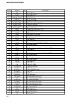
Pin No.
Pin Name
I/O
Description
144
DVDK1
—
Power supply terminal
145
DVS
—
Ground terminal
146
FS256
O
PCM FS256 (Not used)
147
LRCK/WS
I
PCM LRCK (Not used)
148
BCK/SCK
I
PCM BCLK (Not used)
149
ADDT/SDI/GPIOM0
I
PCM ADOUT (Not used)
150
DADT/SDO/GPIOM1
O
Not used
151
MUTFGL/GPIOM2
O
Not used
152
MUTFGR/GPIOM3
O
Model confide (Connected to ground terminal)
153
DVS
—
Ground terminal
154
DVDIO2
—
Power supply terminal
155
DVDIO2
—
Power supply terminal
156
DVS
—
Ground terminal
157
DVDK2
—
Power supply terminal
158
DVS
—
Ground terminal
159
NBOOT
I
Boot mode select (Not used)
160
A0/GPIOA0
O
Address signal (Not used)
161
A1
O
Address signal to FLASH ROM, SRAM
162
A2
O
Address signal to FLASH ROM, SRAM
163
A3
O
Address signal to FLASH ROM, SRAM
164
A4
O
Address signal to FLASH ROM, SRAM
165
A5
O
Address signal to FLASH ROM, SRAM
166
A6
O
Address signal to FLASH ROM, SRAM
167
A7
O
Address signal to FLASH ROM, SRAM
168
A8
O
Address signal to FLASH ROM, SRAM
169
A9
O
Address signal to FLASH ROM, SRAM
170
A10
O
Address signal to FLASH ROM, SRAM
171
A11
O
Address signal to FLASH ROM, SRAM
172
A12
O
Address signal to FLASH ROM, SRAM
173
A13
O
Address signal to FLASH ROM, SRAM
174
A14
O
Address signal to FLASH ROM, SRAM
175
A15
O
Address signal to FLASH ROM, SRAM
176
A16
O
Address signal to FLASH ROM, SRAM
177
AGND
—
Ground terminal
178
ADVREF
—
Reference voltage
179
AVDD
—
Power supply terminal
180
SUBGND
—
for TEST (Connected to ground terminal)
181
MICOUTL
O
MIC signal output (Not used)
182
MICOUTR
O
MIC signal output (Not used)
183
MICINL
I
Tuner signal input
184
MLININL
I
MIC signal input (Not used)
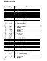
185
MICVREF
—
Reference voltage
186
MICINR
I
Tuner signal input
187
MLININL
I
MIC signal input (Not used)
188
T_ADINR
—
For TEST (Connected to ground terminal)
189
DVS
—
Ground terminal
190
DVDIO2
—
Power supply terminal
191
DVDIO2
—
Power supply terminal
192
DVS
—
Ground terminal


