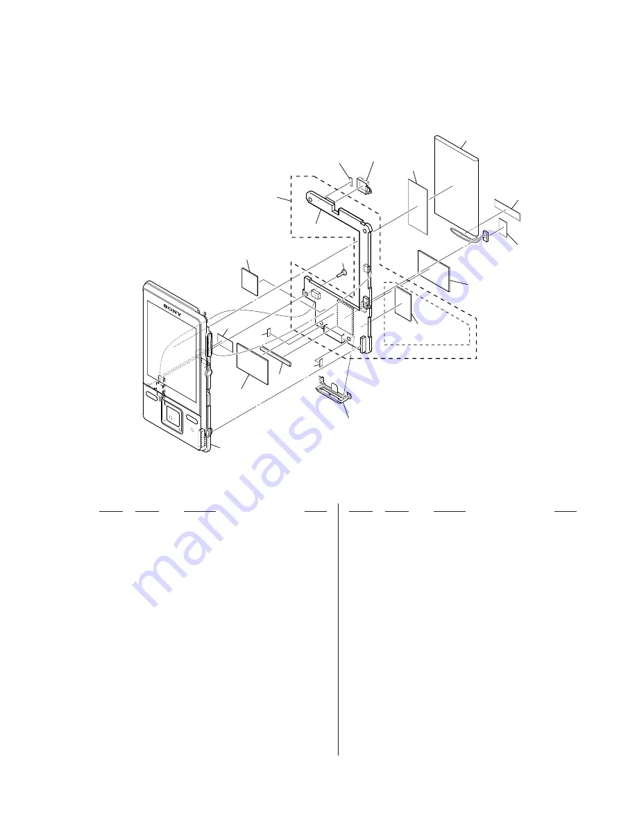
background image

45

NWZ-A826/A826K/A828/A828K/A829

  101 

3-242-558-01  SPACER (LINE IN)

  102 

3-279-346-01  ESCUTCHEON (CN) (for BLACK, GOLD)

  102 

3-279-346-11  ESCUTCHEON (CN) (for WHITE, PINK, SILVER)

  103 

X-2190-606-1  MAIN BOARD, COMPLETE (for SERVICE) (4G) 

(NWZ-A826K: CND)

  103 

X-2190-607-1  MAIN BOARD, COMPLETE (for SERVICE) (8G) 

(NWZ-A828K: US)

  103 

X-2190-608-1  MAIN BOARD, COMPLETE (for SERVICE) (16G) 

(NWZ-A829: US, CND)

  103 

X-2190-609-1  MAIN BOARD, COMPLETE (for SERVICE) (4G) 

(NWZ-A826: FR)

  103 

X-2190-610-1  MAIN BOARD, COMPLETE (for SERVICE) (8G) 

(NWZ-A828: FR)

  103 

X-2190-611-1  MAIN BOARD, COMPLETE (for SERVICE) (16G) 

(NWZ-A829: FR)

  103 

X-2190-612-1  MAIN BOARD, COMPLETE (for SERVICE) (4G) 

(NWZ-A826: AEP, UK, EE/A826K: AEP, UK)

  103 

X-2190-613-1  MAIN BOARD, COMPLETE (for SERVICE) (8G) 

(NWZ-A828: AEP, UK, EE/A828K: AEP, UK)

  103 

X-2190-614-1  MAIN BOARD, COMPLETE (for SERVICE) (16G) 

(NWZ-A829: AEP, UK, EE)

  103 

X-2190-615-1  MAIN BOARD, COMPLETE (for SERVICE) (4G) 

(NWZ-A826: E/A826K: E, AUS)

  103 

X-2190-616-1  MAIN BOARD, COMPLETE (for SERVICE) (8G) 

(NWZ-A828: E)

  103 

X-2190-617-1  MAIN BOARD, COMPLETE (for SERVICE) (16G) 

(NWZ-A829: E, MX, JE)

  103 

X-2190-618-1  MAIN BOARD, COMPLETE (for SERVICE) (4G) 

(NWZ-A826: CH)

  103 

X-2190-619-1  MAIN BOARD, COMPLETE (for SERVICE) (8G) 

(NWZ-A828: CH)

 104 

3-254-136-01 SCREW 

(B1.4)

 105 

3-279-352-01 SHEET 

(BATT), 

ADHESIVE

  106 

1-756-702-11  BATTERY, LITHIUM ION STORAGE 

(E, MX, AUS, CH, JE)

  106 

X-2190-605-1  BATTERY ASSY (US, CND, AEP, UK, FR, EE)

  107 

3-275-663-01  SHEET, BATT WIRE

 108 

3-874-253-01 CUSHION 

(WM-P)

 109 

3-874-254-01 SHEET 

(WM-P)

 110 

3-295-077-01 SPACER 

(PWB-S)

 111 

3-295-078-01 CUSHION 

(PWB)

 112 

3-295-078-11 CUSHION 

(PWB)

 113 

3-873-663-01 SPACER 

(BT-P)

 114 

3-700-202-01 PLATE, 

SHIELD

  Ref. No. 

Part No. 

Description 

Remark

  Ref. No. 

Part No. 

Description 

Remark

6-3.  MAIN  BOARD  SECTION

101

104

103

110

102

101

112

106

107

105

not supplied

(NWZ-A826/A826K)

113

114

108

109

MAIN board

front section

109

111

Summary of Contents for NWZ-A828K Marketing Specifications (NWZ-A828K Black)

Page 1: ...L AND NON COMMERCIAL USE OF A CONSUMER TO i ENCODE VIDEO IN COMPLIANCE WITH THE AVC STANDARD AVC VIDEO AND OR ii DECODE AVC VIDEO THAT WAS ENCODED BY A CONSUMER ENGAGED IN A PERSONAL AND NON COMMERCIAL ACTIVITY AND OR WAS OBTAINED FROM A VIDEO PROVIDER LICENSED TO PROVIDE AVC VIDEO NO LICENSE IS GRANTED OR SHALL BE IMPLIED FOR ANY OTHER USE ADDITIONAL INFORMATION MAY BE OBTAINED FROM MPEG LA L L C...

Page 2: ...P4 file format Wave Riff file format File extension MP3 mp3 WMA 1 wma AAC LC 2 mp4 m4a 3gp Linear PCM wav Codec MP3 Bit rate 32 to 320 kbps Supports variable bit rate VBR Sampling frequency 3 32 44 1 48 kHz WMA 1 Bit rate 32 to 192 kbps Supports variable bit rate VBR Sampling frequency 3 44 1 kHz AAC LC 2 Bit rate 16 to 320 kbps Supports variable bit rate VBR 4 Sampling frequency 3 8 11 025 12 16 ...

Page 3: ...1 IC752 IC901 IC902 AND IC903 ON THE MAIN BOARD REPLACING CN601 CN602 IC301 IC302 IC305 IC453 IC501 IC503 IC508 IC509 IC601 IC602 IC701 IC751 IC752 IC901 IC902 and IC903 on the MAIN board cannot exchange with single When CN601 CN602 IC301 IC302 IC305 IC453 IC501 IC503 IC508 IC509 IC601 IC602 IC701 IC751 IC752 IC901 IC902 and IC903 on the MAIN board are damaged exchange the entire mounted board NOT...

Page 4: ...ration by pressing the BACK HOME button in step or Note Do not format the built in flash memory using software or Windows Explorer Press the button to select Common Settings and then press the button to confirm The list of Common Settings options appears Press the button to select Format and then press the button to confirm All data including songs will be deleted Proceed appears Press the button ...

Page 5: ...function VOL 2 button Adjusts the volume BLUETOOTH button Press and hold to turn on or off the Bluetooth function and to establish or to end Bluetooth connection HOLD switch You can protect the player against accidental operation by using the HOLD switch when carrying it By sliding the HOLD switch to the direction of the arrow all operation buttons are disabled If you slide the HOLD switch to the ...

Page 6: ...LOW Note Follow the disassembly procedure in the numerical order given 3 2 COVER REAR REAR ASSY SET 3 2 COVER REAR REAR ASSY Page 6 3 3 BATTERY Page 7 3 4 MAIN BOARD Page 7 3 5 LCD ASSY Page 8 two screws M1 4 R two ornamental screws screw M1 4 RB two claws RT rear assy RB two claws lid ACC claw claw claw window LED cover rear ...

Page 7: ...nnector please be careful about the color of the lead wires as shown in a figure and install battery connector screw B1 4 spacer line in claw BATT wire sheet R connector CN601 connector board to board connector board to board spacer line in connector CN901 HP flexible print board CN301 RL MAIN board RB cushion PWB sheet key CN602 escutcheon CN RI spacer BT P RK shield plate RT spacer PWB S RE shee...

Page 8: ...rd LCD flexible board CN801 sheet LCD B two screws B1 4 screw B1 4 RE LCD assy R Open the LCD assy in the direction of the arrow waterproof jack J301 Remove the waterproof jack J301 in the direction of the arrow RB boss RT Pull out the LCD flexible board LCD flexible board LCD assy Front block Front block ...

Page 9: ...TCHK DAC BLUETOOTH SHUTDOWN EXITTEST 4 1 1 Power supply voltage check This mode is used in case power supply voltage in the state where all power supply lines are starting is checked Checking method 1 Enter the test mode 2 Press the v V key to select the POWER and press the B key to enter the minor item 3 Press the v V key to select the VCHK 4 Press the u key all power supply lines are started liq...

Page 10: ...te each time the OPTION key is pressed the port setting for the charge is changed as shown in the table below Port control Display CHG_XCHGEN CHG_PEN1 CHG_PEN2 AC L H H USB500 L H H USB100 L H L 6 Press the BACK key return to minor item selection screen 4 1 5 Battery voltage detection check This mode is used in case battery voltage is checked Checking method 1 Enter the test mode 2 Press the v V k...

Page 11: ...finity Zero HPOUT VOL 30 START 5 Press the BACK key return to minor item selection screen 4 2 3 Frequency characteristic 1 check 20 Hz 0 dBs L ch R ch VOLUME 25 audio signal is output ted Checking method 1 Enter the test mode 2 Press the v V key to select the AUDIO and press the B key to enter the minor item 3 Press the v V key to select the F1 4 Press the u key 20 Hz 0 dBs L ch R ch VOLUME 25 aud...

Page 12: ... Maximum output check 1 kHz 0 dBs L ch R ch VOLUME 30 Headphone output when AVLS operates 1 kHz 0 dBs L ch R ch VOLUME 13 audio signal is outputted Checking method 1 Enter the test mode 2 Press the v V key to select the AUDIO and press the B key to enter the minor item 3 Press the v V key to select the MAXOUT 4 Press the u key 1 kHz 0 dBs L ch R ch VOLUME 30 Headphone output when AVLS operates 1 k...

Page 13: ...lt Color bar standard Color bar bright ness minimum Color bar brightness maxmum All red All green All blue All white Maximum drawing size confirmation diagonal gradation red diagonal gra dation green diagonal gradation blue diagonal grada tion white Maximum drawing size confirmation All blue All sides are red is displayed Whether red in all sides is seen is confirmed 5 In this state each time the ...

Page 14: ... s area is formatted and ICV for the video and ICV for audio are initialized Note Not used for the servicing Format the set from Settings Common settings For mat when it home menu in usually operates when the set should format it 4 4 5 Destination setting The destination setting language information and sound pressure regulation information are written in the NAND flash memory Note Not used for th...

Page 15: ...he vender ID at 1 5 Press the BACK key return to minor item selection screen 4 5 CLESTE liquid crystal display MPTAPP MENU POWER AUDIO VIDEO OTHER CLESTE WCABLE DAC WOCABLE BLUETOOTH SHUTDOWN EXITTEST 4 5 1 Clear stereo setting With cable This mode is according to an original sound playback for adjust ment to right and left sound Note Not used for the servicing 4 5 2 Clear stereo setting No cable ...

Page 16: ... power setting Bluetooth transmitting power is set If the test mode is released the transmitting power set in this mode becomes invalid Note Not used for the servicing 4 7 4 Bluetooth connection check It connects with the address selected by SETADR with the chan nel set by SETCH and the result is displayed Note Not used for the servicing 4 8 Shutdown Function that power supply of set can be turned...

Page 17: ...A1 H8 SDR_CLK AA5 CLK J1 SDR_CSZ0 T3 CS J8 SDR_CKE0 T1 CKE J2 SDR_WEZ R5 WE K8 SDR_CASZ U8 CAS K7 SDR_RASZ T5 RAS J9 SDR_DQM0 P5 DQM0 K9 SDR_DQM1 R4 DQM1 K1 SDR_DQM2 R3 DQM2 F8 SDR_DQM3 R2 DQM3 F2 A0 A12 SDR_D0O SDR_D31 SDR_A00 SDR_A12 NAND FLASH MEMORY IC751 NAND_DA0 NAND_DA7 NAND_ALE D3 I O1 I O8 ALE 17 NAND_CLE E9 CLE 16 NAND_CEZ0 M9 XCE1 9 NAND_CEZ1 C2 XCE2 10 NAND_CEZ2 B3 NAND_CEZ3 C3 NAND_RE...

Page 18: ..._J 23 LX1 20 EN 31 Y2 CISET 12 DOK CHG_XCHGEN 10 V10 CEN CHG_PEN2 40 W8 PEN2 USB_SUSPEND 1 AB8 USUS XCHG_DET 39 AC4 CST1 CHG_XFLT 37 AB4 CRD_AD C8 CST2 VOLTAGE DETECT IC902 CHARGE CONTROL Q901 3 1V REGULATOR IC602 1 8V REGULATOR IC504 3 1V REGULATOR IC503 HP WM PORT 1 8V 1 8V REGULATOR IC301 VDD_BT1 8_ 1 8V REGULATOR IC903 VDD_ANA_F VDD_ECO_J VDD_GP1_J VDD_GP1_FB_J VDD_GP3 VDD_GP5 VDD_HP_F VDD_LO_...

Page 19: ...oduction tolerances Voltages are taken with VOM Input impedance 10 MΩ Voltage variations may be noted due to normal production tolerances Circled numbers refer to waveforms Signal path F AUDIO L VIDEO The voltage and waveform of CSP chip size package cannot be measured decause its lead layout is different form that of conventional IC For Printed Wiring Boards Note X Parts extracted from the compon...

Page 20: ... 5 1 3 4 A1 B1 C1 D1 E1 F1 G1 H1 J1 K1 L1 M1 N1 P1 R1 A2 B2 C2 D2 E2 F2 G2 H2 J2 K2 L2 M2 N2 P2 R2 A3 B3 C3 D3 E3 F3 G3 H3 J3 K3 L3 M3 N3 P3 R3 A7 B7 C7 D7 E7 F7 G7 H7 J7 K7 L7 M7 N7 P7 R7 A8 B8 C8 D8 E8 F8 G8 H8 J8 K8 L8 M8 N8 P8 R8 A9 B9 C9 D9 E9 F9 G9 H9 J9 K9 L9 M9 N9 P9 R9 2 4 3 1 K K R210 FB608 R601 R606 R607 R608 R220 C216 R223 R611 R615 R616 R617 R618 R619 CN601 R620 R621 R622 R623 R624 R6...

Page 21: ...1 R853 R855 R857 R858 R859 R667 R862 C633 C634 R671 D201 C853 C854 TB301 R105 R302 R304 R305 R503 R310 R504 R505 R312 R314 R315 TB901 R510 CN301 R511 R901 R904 R907 R520 R908 R521 R522 R910 R911 R913 C107 R914 R916 C301 C302 C303 CN901 C306 C308 C310 C311 C312 C313 C314 C315 C316 C511 C512 C516 C517 C518 C326 C327 C328 C329 C908 C909 R751 R753 C330 R754 R755 R756 R757 C910 R758 R759 R760 R761 R762...

Page 22: ..._LINEOUT PCM0_DADT WAKEUP_INT CHG_ICTL CRD_AD AB0_A1 AB0_A3 AB0_A4 AB0_A5 AB0_A6 AB0_A7 AB0_A8 AB0_XCS2 AB0_D0 AB0_D1 AB0_D10 AB0_D11 AB0_D12 AB0_D13 AB0_D14 AB0_D15 AB0_D2 AB0_D3 AB0_D4 AB0_D5 AB0_D6 AB0_D7 AB0_D8 AB0_D9 AB0_XRD AB0_XWR RESETZ AB0_XCS2 AB0_XRD AB0_XWR AB0_A1 AB0_A2 AB0_A3 AB0_A4 AB0_A5 AB0_A6 AB0_A8 AB0_D0 AB0_D1 AB0_D2 AB0_D3 AB0_D4 AB0_D5 AB0_D6 AB0_D7 AB0_D8 AB0_D9 AB0_D10 AB0...

Page 23: ...SDR_D14 SDR_XCS0 SDR_CKE0 SDR_D27 SDR_D04 SDR_D02 SDR_A06 SDR_D05 SDR_D28 SDR_D15 SDR_DQM0 SDR_A10 SDR_D16 SDR_D06 SDR_D24 SDR_BA0 SDR_D13 SDR_D17 SDR_D11 SDR_DQM3 SDR_D23 SDR_D12 SDR_D22 SDR_D25 SDR_DQM1 SDR_D30 SDR_D09 SDR_D07 SDR_XRAS SDR_D01 SDR_D08 SDR_XCAS SDR_A04 SDR_CLK SDR_D31 SDR_A08 SDR_D26 SDR_A01 C701 0 1 DGND C703 0 1 C705 0 1 C707 0 1 C709 0 1 C711 0 1 C713 0 1 VDD_ECO_J FL701 100k ...

Page 24: ...781 NAND_RXB1 NAND_XCS1 0 R758 0 R757 R760 0 0 R761 0 R762 R763 0 470k R759 NAND_ALE NAND_CLE NAND_XRD NAND_XCS3 NAND_XCS2 NAND_D07 NAND_D06 NAND_D05 NAND_CLE NAND_ALE NAND_XWR NAND_D02 NAND_D00 NAND_D04 NAND_D01 NAND_D03 NAND_RXB2 NAND_RXB0 NAND_XWP NAND_RXB0 NAND_XRD NAND_XCS0 NAND_CLE NAND_ALE NAND_XWR NAND_XWP NAND_RXB1 NAND_XCS1 NAND_RXB1 NAND_XCS1 NAND_RXB1 NAND_RXB2 NAND_XRD NAND_XCS2 NAND_...

Page 25: ...AB0_D6 AB0_D5 AB0_D4 AB0_D10 AB0_D8 AB0_D9 AB0_D11 AB0_D15 AB0_D12 AB0_D14 AB0_D13 AB0_A1 AB0_A2 AB0_A3 AB0_A4 AB0_A7 AB0_A6 AB0_A5 AB0_A8 USB_INT IC503 TK63731AB1G0B A1 GND B1 VOUT B2 VIN A2 VCONT PSM_L0DET VDD_UNREG_J C504 0 1 C511 1 R511 220k RESETZ C510 0 1u USB_DP USB_DM VCC_VBUS C512 1 C506 0 1 USB_XRST R519 220k IC502 TC7SG08AFS 1 2 GND 3 4 5 VCC IC504 TK63718HCL G 1 VIN 2 GND 3 VOUT 4 NC 5...

Page 26: ... Q303 EMX18 1 2 Q301 UNR31A600LS0 C305 10 IC301 XC6401FF58DR 1 2 3 4 5 6 7 C307 10 R310 0 R312 0 R302 0 C319 4 7 C321 0 022 Q304 UNR31A600LS0 R314 0 CL101 CL201 PCM0_BCK PCM0_ADDT FB201 FB301 FB101 PCM0_LRCK IC305 MAX4745ELB TG069 1 CB1 2 NO1 3 GND 4 NO2 5 CB2 6 COM2 7 NC2 8 VCC 9 NC1 10 COM1 C208 0 1 R106 R106 206 5 6 EXCEPT NWZ A826 FR A828 FR A829 FR 43 NWZ A826 FR A828 FR A829 FR R206 11P CN30...

Page 27: ...RT_TXD B2 UART_RXD B3 UART_CTS B4 PIO8 B5 VCC_IO B6 VCC C1 PCM_OUT C2 PCM_SYNC C3 GND C4 AIO0 C5 RESETB C6 VCC_18V D2 PCM_IN D3 PIO5 D4 PIO0 D5 PIO3 D6 GND E1 USB_DN E2 USB_DP E3 PIO4 D1 PCM_CLK E4 PIO1 E6 RF_IO F4 PIO2 F1 GND F2 PIO6 F3 NC F5 GND E5 GND TC7PA53FU TE85L F IC452 1 CH1 2 GND 3 CH0 4 COMON 5 VCC 6 A TC7PA53FU TE85L F IC451 1 CH1 2 GND 3 CH0 4 COMON 5 VCC 6 A UART_TXD VDD_UNREG_J BT_L...

Page 28: ...1 C917 CL910 CL911 CL912 CL913 CL915 CL916 0 001 C924 10 C925 0 R935 MAX8671CETL TG069 IC901 1 USUS 2 DC 3 USB 4 FB5 5 PV5 6 OUT5 7 PG2 8 LX2 11 FB2 12 DOK 13 REG3L 14 BP 15 OUT4 16 PV4 21 SSKP 22 PV1 23 LX1 24 PG1 31 CISET 32 CT 41 EP 33 THM 34 BAT 35 SYS 36 PEN1 37 CST2 38 UOK 39 CST1 40 PEN2 9 PV2 10 CEN 17 BVSET 18 GND 19 FB1 20 EN 25 PG3 26 LX3 27 PV3 28 VL 29 FB3 30 DISET 0 R931 0 R930 0 R92...

Page 29: ...805 FB806 FB807 FB808 FB809 FB810 FB811 FB812 FB813 C807 C808 JL801 JL802 JL803 JL804 JL805 R881 R882 R883 R884 R887 R888 C881 C882 S890 S891 S892 S893 S894 S895 S896 CL888 17 1 4 5 8 S G D 12 9 16 13 R801 R803 FB814 R804 FB815 FB816 FB817 FB818 R808 FB819 R809 R810 CN801 R829 R830 R831 1 2 39 38 C801 C803 C804 C805 C806 CN881 41 42 1 2 IC801 Q801 FL801 SW BOARD SIDE A SW BOARD SIDE B 1 875 442 11...

Page 30: ...CD_ENABLE LCD_PXCLK DGND VDD_UNREG_J 100 R888 LCD_G3 LCD_G2 LCD_G1 LCD_G0 LCD_HSYNC LCD_VSYNC LCD_PON VDD_ANA_F VDD_LOG_F 42P CN881 1 KEY_AD0 3 KEY_AD1I 5 SPI0_LCD_XCS 7 DGND 9 LCD_BLTCTL 11 LCD_PWM1 13 DGND 15 VDD_UNREG_J 17 LCD_B0 19 LCD_B1 21 LCD_B2 23 LCD_B3 25 LCD_B4 27 LCD_B5 29 LCD_ENABLE 31 LCD_PXCLK 33 LCD_HSYNC 35 LCD_VSYNC 37 LCD_PON 39 VDD_ANA_F 41 VDD_LOG_F 2 KEY_GND 4 KEY_AD1O 6 KEY_...

Page 31: ...C807 FB811 LCD_G2 LCD_B1 LCD_R0 FB805 LCD_B0 0 22 C801 LCD_R4 LCD_R2 LCD_HSYNC FB818 JL802 LCD_G5 VDD_LOG_F FB812 LCD_B2 0 47 C804 FB806 LCD_G3 LCD_G4 LCD_VSYNC JL803 FB819 SSM3K15FV TL3SONYZ Q801 S LCD_G1 LCD_B3 FB813 JL804 LCD_PXCLK FB807 SPI0_MOSI 3300 R804 VDD_UNREG_J 100k R830 VDD_ANA_F FL801 JL801 LCD_ENABLE 1 C803 FB814 SPI0_LCD_XCS 100k R829 0 R810 FB808 FB802 TPS60231RGTR IC801 1 ISET 2 N...

Page 32: ...D LOCAL SYNTH CLOCK GENERATION IC501 S1R72V27B05E10B B8 CHANNEL OSCILLATOR USB NC CPU INTERFACE CONTROLLER MULTI TRANSCELVER FIRST IN FIRST OUT C8 F3 H2 E3 G4 F4 E1 C5 E2 D3 G1 F1 F2 H4 A1 C6 E8 D6 F8 E7 F7 G8 XWRH CD0 CA8 CA7 CA6 CA5 CA4 CA3 CA2 XDACK XDREQ XINT XCS CD15 CD14 CD13 CD12 CD11 CD10 CD9 XI XO G3 XRD TEST MUX H1 TESTEN H8 ATPGEN A8 BURNIN MACRO DEVICE SERIAL INTERFACE ENGINE HOST SERI...

Page 33: ...PV3 26 LX3 25 PG3 24 PG1 23 LX1 22 PV1 21 SSKP 4 FB5 5 PV5 6 OUT5 7 PG2 8 LX2 9 PV2 20 EN 16 PV4 15 OUT4 14 BP 11 FB2 3 USB 34 BAT 10 CEN 3 3V LOW DROPOUT HIGHEST VOLTAGE SELECTOR REG1 DC DC CONVERTER REG3 DC DC CONVERTER REG4 LOW DROPOUT REG5 LOW DROPOUT REG2 DC DC CONVERTER 14 GND 15 EN1 16 EN2 13 VIN 11 C1 12 C2 10 C1 9 C2 2 NC 1 ISET 3 NC 4 D3 6 D1 5 D2 8 VOUT 7 PGND CHARGE PUMP CURRENT SINKS ...

Page 34: ...nector 12 VA Power supply terminal 1 8V 13 AGND Ground terminal 14 DAC_FILT O Positive reference voltage output terminal 15 VQ O Quiescent voltage output terminal 16 ADC_FILT O Positive reference voltage output terminal 17 MICIN1 AIN3A I Microphone signal input terminal Not used 18 MICIN2 AIN3B BIAS I Microphone signal input terminal Not used 19 AIN2A I Analog audio L ch signal input terminal Not ...

Page 35: ...13 SWGND Ground terminal B14 NC Not used B15 SWADP2 Not used B16 GND Ground terminal B17 VCCADP I Power supply input terminal 5V B18 NC Not used B19 IO_A Not used B20 VDD_L0 I Power supply input terminal 1 2V B21 to B26 NC Not used C1 NC Not used C2 NAND_CEZ1 O Chip enable signal output to the NAND flash memory NWZ A828 A828K A829 only C3 NAND_CEZ3 O Chip enable signal output to the NAND flash mem...

Page 36: ...IO_B Not used E6 NAND_DA5 I O Two way data bus with the NAND flash memory E7 NC Not used E8 NAND_DA7 I O Two way data bus with the NAND flash memory E9 NAND_CLE O Command latch enable signal output to the NAND flash memory E10 BATSEL Not used E11 SWBAT Not used E12 CAPBTDL Not used E13 CAPADDL Not used E14 NC Not used E15 SWVBUS Not used E16 E17 NC Not used E18 AB0_A4 O Address signal output to th...

Page 37: ...used J11 to J17 GND Ground terminal J18 NC Not used J19 AB0_RDZ O Read strobe signal output to the USB controller J22 to J24 AB0_D10 to AB0_D12 I O Two way data bus with the USB controller J25 CHGGND1 Ground terminal J26 NC Not used K1 to K3 VDD_L1 I Power supply input terminal 1 2V K4 K5 SDR_DATA28 SDR_DATA26 I O Two way data bus with the SD RAM K8 NAND_RBZ3 O Read busy signal output to the NAND ...

Page 38: ...rystal display P24 NC Not used P25 P26 IO_A Not used R1 SDR_DATA0 I O Two way data bus with the SD RAM R2 to R4 SDR_DQM3 to SDR_DQM1 O Write mask signal output to the SD RAM R5 SDR_WEZ O Write enable signal output to the SD RAM R8 SDR_DATA1 I O Two way data bus with the SD RAM R9 GND Ground terminal R10 NC Not used R17 U70_CTSZ O CTS signal output to the bluetooth controller R18 U70_RTSZ I RTS sig...

Page 39: ...l output to the LED control V18 UART_SEL O Serial data select signal output to the multiplexer V19 NCHP_DET I Headphone detection signal input terminal Not used V22 C_RTCK I Clock signal input terminal for JTAG V23 C_TRSTZ I Reset signal input terminal for JTAG V24 VPLLIN I Power supply input terminal 2V V25 VDSPIN I Power supply input terminal 2 9 4 2V V26 VDSP Not used W1 IOGND Ground terminal W...

Page 40: ...converter AB23 AB24 GND Ground terminal AB25 GND1 Ground terminal AB26 OSCIN I Sub system clock input terminal 32 768 kHz AC1 to AC3 IO_A Not used AC4 XCHG_DET I Charge detection signal input from the power control AC5 USB_INT1 I Interrupt request signal input from the USB controller AC6 SPIO_XCS0 O Chip select signal output to the liquid crystal display AC7 SPI0_SK O Serial data transfer clock si...

Page 41: ... 1 8V AE5 DD2GNDA Ground terminal AE6 DD2INA I Power supply input terminal 2 9 4 2V AE7 VDD_L0 I Power supply input terminal 1 2V AE8 VDD_L1 I Power supply input terminal 1 2V AE9 IO_C Not used AE10 AE11 NC Not used AE12 DD1INA I Power supply input terminal 2 9 4 2V AE13 IO_B Not used AE14 AVDD_LPLL I Power supply input terminal 1 2V AE15 AVDD_HPLL I Power supply input terminal 1 2V AE16 GND Groun...

Page 42: ... DD1INB2 I Power supply input terminal 2 9 4 2V AF18 DD1VFBK2 I Power supply voltage feedback terminal AF19 DD1GNDA Ground terminal AF20 VGP1 O Power supply output terminal 2 85V AF21 COM Not used AF22 NC Not used AF23 VGP3 O Power supply output terminal 2 85V AF24 to AF26 NC Not used ...

Page 43: ...ardized parts so they may have some difference from the original one Items marked are not stocked since they are seldom required for routine ser vice Some delay should be anticipated when ordering these items The mechanical parts with no reference number in the exploded views are not sup plied Color Indication of Appearance Parts Ex ample KNOB BALANCE WHITE RED R R Parts Color Cabinet s Color Acce...

Page 44: ...1 REAR ASSY PINK NWZ A828 EE 51 X 2190 890 1 REAR ASSY GOLD NWZ A828 EE 51 X 2190 891 1 REAR ASSY BLACK NWZ A828 CH 51 X 2190 892 1 REAR ASSY BLACK NWZ A828 E 51 X 2190 893 1 REAR ASSY PINK NWZ A828 E 51 X 2190 894 1 REAR ASSY BLACK NWZ A829 AEP UK 51 X 2190 895 1 REAR ASSY GOLD NWZ A829 AEP UK 51 X 2190 896 1 REAR ASSY BLACK NWZ A829 FR 51 X 2190 897 1 REAR ASSY GOLD NWZ A829 FR 51 X 2190 898 1 R...

Page 45: ...6G NWZ A829 AEP UK EE 103 X 2190 615 1 MAIN BOARD COMPLETE for SERVICE 4G NWZ A826 E A826K E AUS 103 X 2190 616 1 MAIN BOARD COMPLETE for SERVICE 8G NWZ A828 E 103 X 2190 617 1 MAIN BOARD COMPLETE for SERVICE 16G NWZ A829 E MX JE 103 X 2190 618 1 MAIN BOARD COMPLETE for SERVICE 4G NWZ A826 CH 103 X 2190 619 1 MAIN BOARD COMPLETE for SERVICE 8G NWZ A828 CH 104 3 254 136 01 SCREW B1 4 105 3 279 352 ...

Page 46: ... 279 351 01 CONNECTOR A RUBBER 162 1 875 533 11 HP FLEXIBLE PRINT BOARD 163 3 279 342 01 PLATE HP FIXED 164 3 254 135 01 SCREW B1 4 165 3 398 056 01 SHEET LCD B 166 3 254 136 01 SCREW B1 4 167 3 874 255 01 SHEET WR 168 3 279 340 01 CHASSIS MAIN 169 1 798 110 11 KEY SHEET 170 3 289 896 01 SPACER HP 171 3 874 258 01 SPACER WM P 172 3 874 838 01 SHEET COVER HP 173 3 279 333 01 LIGHT GUIDE 174 3 279 3...

Page 47: ...C453 1 114 821 21 CERAMIC CHIP 1 8PF 0 1PF 50V C455 1 164 943 81 CERAMIC CHIP 0 01uF 10 16V C456 1 125 777 11 CERAMIC CHIP 0 1uF 10 10V C457 1 100 742 91 CERAMIC CHIP 2 2uF 20 10V C458 1 165 884 11 CERAMIC CHIP 2 2uF 10 6 3V C459 1 164 931 11 CERAMIC CHIP 100PF 10 50V C501 1 164 856 81 CERAMIC CHIP 18PF 5 50V C502 1 164 854 11 CERAMIC CHIP 15PF 5 50V C503 1 100 352 91 CERAMIC CHIP 1uF 20 16V C504 ...

Page 48: ...AMIC CHIP 0 1uF 10 6 3V C754 1 112 716 11 CERAMIC CHIP 0 1uF 10 6 3V NWZ A828 A828K A829 C755 1 112 716 11 CERAMIC CHIP 0 1uF 10 6 3V NWZ A828 A828K A829 C853 1 128 622 91 CERAMIC CHIP 100PF 10 16V C854 1 164 943 81 CERAMIC CHIP 0 01uF 10 16V C855 1 164 935 11 CERAMIC CHIP 470PF 10 50V C856 1 100 415 91 CERAMIC CHIP 0 47uF 10 6 3V C902 1 100 670 11 CERAMIC CHIP 4 7uF 20 16V C903 1 112 746 11 CERAM...

Page 49: ...218 949 11 RES CHIP 470 5 1 16W R210 1 244 161 81 RES CHIP 2 2 5 1 16W R220 1 240 691 91 METAL CHIP 470 5 1 20W R223 1 218 990 81 SHORT CHIP 0 R252 1 240 718 91 METAL CHIP 100K 5 1 20W R256 1 240 726 91 METAL CHIP 470K 5 1 20W R302 1 218 990 81 SHORT CHIP 0 R304 1 240 720 91 METAL CHIP 150K 5 1 20W R305 1 240 722 91 METAL CHIP 220K 5 1 20W R307 1 240 695 91 METAL CHIP 1K 5 1 20W R310 1 218 990 81 ...

Page 50: ...0 81 SHORT CHIP 0 NWZ A829 R758 1 218 990 81 SHORT CHIP 0 NWZ A829 R759 1 240 726 91 METAL CHIP 470K 5 1 20W R760 1 218 990 81 SHORT CHIP 0 NWZ A828 A828K R761 1 218 990 81 SHORT CHIP 0 NWZ A829 R762 1 218 990 81 SHORT CHIP 0 NWZ A829 R763 1 218 990 81 SHORT CHIP 0 NWZ A828 A828K R764 1 240 726 91 METAL CHIP 470K 5 1 20W R765 1 240 718 91 METAL CHIP 100K 5 1 20W R767 1 240 718 91 METAL CHIP 100K 5...

Page 51: ...1 SMD EMI FERRITE FB814 1 481 258 21 SMD EMI FERRITE FB815 1 481 258 21 SMD EMI FERRITE FB816 1 481 258 21 SMD EMI FERRITE FB817 1 481 258 21 SMD EMI FERRITE FB818 1 481 258 21 SMD EMI FERRITE FB819 1 481 258 21 SMD EMI FERRITE FILTER FL801 1 234 939 21 FILTER EMI REMOVAL SMD IC IC801 Not supplied IC TPS60231RGTR FET Q801 6 550 789 01 FET SSM3K15FV TL3SONYZ RESISTOR R801 1 208 699 11 METAL CHIP 4 ...

Page 52: ...0 31 MANUAL QSG INSTRUCTION Quick Start Guide GERMAN NWZ A826 AEP UK NWZ A826K AEP NWZ A828 AEP UK NWZ A828K AEP NWZ A829 AEP UK 3 289 810 41 MANUAL QSG INSTRUCTION Quick Start Guide SPANISH NWZ A826 AEP UK NWZ A826K AEP NWZ A828 AEP UK NWZ A828K AEP NWZ A829 AEP UK MX 3 289 810 51 MANUAL QSG INSTRUCTION Quick Start Guide ITALIAN NWZ A826 AEP UK NWZ A826K AEP NWZ A828 AEP UK NWZ A828K AEP NWZ A829...

Page 53: ...MEMO NWZ A826 A826K A828 A828K A829 53 ...

Page 54: ...29 REVISION HISTORY Checking the version allows you to jump to the revised page Also clicking the version at the top of the revised page allows you to jump to the next revised page Ver Date Description of Revision 1 0 2008 03 New ...

Reviews: