3-12
PCS-1500/1500P
[CPU block]
In the CPU block, the Hitachi SH-3 (HD6417708) CPU (IC100) is used in the following modes of operation.
Clock operation mode : Mode 1 (pin-MD0 = High, pin-MD1 = Low, pin-MD2 = Low)
With EXTAL input = 7.5 MHz, CKIO output = 30 MHz and
internal clock = 60 MHz
It is assumed that the FRQCR register value of the SH-3 is set to
0x0111 (or 0x0191).
Memory bus width :
32 bits (pin-MD3 = High, pin-MD4 = High)
The bus width of area 0 immediately after the power-on reset is set to 32
bits.
Data format :
Big Endian (pin-MD5 = Low)
The order of the bytes of the data is set to big endian.
The other detailed mode setups are set by the internal register.
The above-described mode is set according to the state of pin-MD0 to pin-MD5 when the CPU is reseting
(these pins are used for other purposes in modes other than reset.) Because most pins are used as output
pins during normal operation (used as input pins during reset), connecting the pull-up resistors or pull-
down resistors is sufficient for setting. However, because pin-MD2 is used as the input pin (RXD) during
normal operation, the source IC that inputs the signal to pin-MD2 must be controlled to supply the desired
level to this pin during reset. In the CPU block, output of the line driver (IC200) that is connected to pin-
MD2/RXD is controlled to be high impedance when the CPU is reseting.
SH-3 has a built-in timer, interrupt controller, memory controller, real-time clock and serial controller.
Therefore, the SH-3 can be operated by connecting memories only. The operating status of the CPU can
be output to terminals by connecting the line driver/receiver to the serial controller input/output. At the
same time, because the PCMCIA interface bus cycle can be generated, the PCMCIA interface can be
realized by adding buffers and some I/O ports only.
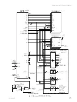
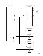
Fig. 3-6 shows the connection between the CPU, memories and the PCMCIA buffers.
As the memory, two (IC103, IC104) 32-Mbit (2 M
x
16-bit) flash memories and two (IC101, IC102) 64-
Mbit (1M
x
16-bit
x
4 banks) synchronous DRAMs are used. The flash memories are used for storing
the program and parameters. SDRAMs are used as the work area.
The operating clock (7.5 MHz) is supplied from X100. The clock signal (32.768 kHz) for the real-time
clock is generated by using the externally connected crystal oscillator (X101).
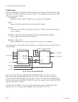
The reset signal for the CPU and flash memories is generated by monitoring the
+
3.3 V potential with the
power voltage watchdog IC (IC115). The flash memory requires 20 microseconds after it is reset until it
can be operated. It means that a sufficient delay time must be given to the reset signal that is input to the
CPU so that the flash memory data can be read immediately after the CPU starts up.
The input and output ports of the serial controller are connected to the Diagnostics port via the line driver/
receiver (IC200). This enables the diagnostics software to be operated by activating the minimum
circuitry around the CPU. The diagnostics serial port consists of the data transmission and reception lines
only, and no control lines.
The PCMCIA interface consists of the buffers operating on the
+
3.3 V-2 power that are connected to the
SH-3 bus signal. The three output ports, seven input ports (including the power supply current monitor-
ing information), interrupt and bus wait signal are used in addition to the SH-3 bus.
3-2. Circuit Description of the Respective Boards
Summary of Contents for PCS-1500
Page 8: ......
Page 75: ...1 67 PCS 1500 1500P Sony Corporation Printed in Japan ...
Page 76: ......
Page 130: ......
Page 198: ......


