3-14
PCS-1500/1500P
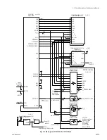
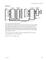
Fig. 3-7 shows the buses signals that control the respective blocks.
The block controlling buses are divided into the 5 V bus and 3.3 V bus.
5 V bus :
The bus line that controls the block that operates on
+
5 V power.
The UART, BRI and NETIF blocks and optional board. They operate even in the
Standby state.
3.3 V bus : The bus line that controls the block that operates on
+
3.3 V-2 power.
The VCP, VIDDA, AC and EC blocks. They do not operate in the Standby state.
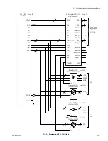
The bus control PLD (IC110) has the following functions:
.
Power supply control and reset control
.
Generation of the buffer control signals that are suited to the bus cycle generated by the CPU
.
Generation of the device access control signals
.
Bus wait control for the CPU
.
Encoding of the interrupt priority levels and interrupt control such as masking some interrupts.
.
A part of the PCMCIA interface control
The optimum setup for the bus cycle of each block, which the CPU has generated, is performed by the
register inside the CPU.
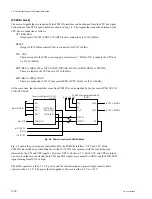
The circuitry whose power is turned off during the Standby state is connected the IC110 via the bus
switches (IC111, IC112) that operate on
+
3.3 V-2 power.
The operating power supply voltage is
+
3.3 V. The circuit blocks whose power is turned off during the
Standby state and the interface buffers operate on
+
3.3 V-2 power.
3-2. Circuit Description of the Respective Boards
Summary of Contents for PCS-1500
Page 8: ......
Page 75: ...1 67 PCS 1500 1500P Sony Corporation Printed in Japan ...
Page 76: ......
Page 130: ......
Page 198: ......


