3-19
PCS-1500/1500P
[BRI block]
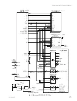
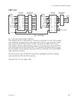
The BRI block performs the BRI-2B line control and data transmitting/receiving. The BRI block consists of the following
devices. The I-Interface control IC (IC800) as the central component of this block, the 256-kbit SRAM (IC801) where the
firmware for the I-Interface control IC (IC800) is stored, the 256-kbit SRAM (IC802) that is a work area RAM, the bus
signal selector buffers (IC810, IC811) and SRAM address setting latches (IC808, IC809) that are used to download the
firmware to SRAM from the CPU, the latch circuit (IC806, IC805, IC803) to generate interrupts and to output the status to
the CPU from the I-Interface control IC (IC800), and the circuit (IC803, IC804, IC807, IC812) to generate the signals that
control the above-described circuit in response to the access from the CPU. (Refer to Fig. 3-11.)
Because the I-Interface control IC (IC800) starts its operation by executing the program codes that are stored in the SRAM
(IC801), the firmware must be downloaded to the SRAM (IC801) beforehand from the CPU. Downloading is performed
by the following setup.
(1) Setting the SRAM interface output of the I-Interface control IC (IC800) to Hi-Z by putting the “RES_BRI” and
“MODE_SET” signals active.
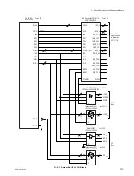
(2) Connecting the CPU system bus with the SRAM (IC801) via the bus signal selector buffer (IC810, IC811) and the
SRAM address setting latches (IC808, IC809) by putting the “DOWNLOAD” signal active.
(3) Repeating writing the SRAM address into the latches (IC808, IC809) and writing the program code into the SRAM.
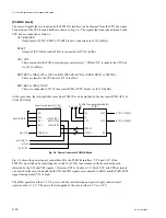
The interrupt signal to the CPU from the I-Interface control IC (IC800) is created when the I-Interface control IC (IC800)
writes into the latch circuit (IC806, IC805, IC803) using the SRAM interface. This interrupt signal is once input into
IC750 of the NETIF block and is multiplexed with the other interrupts, then is output as “IRQ_TDM”. The interrupt signal
is cleared when the “SDETCLR” signal goes active when the CPU reads the specific address. The interrupt signal status
and the result of the SRAM check by the I-Interface control IC (IC800) can be read out from the CPU via the buffer
(IC758). The information on which the broadcast video format (NTSC or PAL) is specified and whether the camera (PCS-
C150/C150P) is connected to the processor directly or not can be obtained by reading this buffer (IC758).
The interface with the telephone line contains a choke coil (FL800) as a countermeasure against EMI and pulse transform-
ers (T201, T202) between the modular jack (CN800) and the I-Interface control IC (IC800).
The line data is converted to two pairs (A pair for transmission and reception respectively) of data that is synchronized with
64 kHz, and is transferred between the I-Interface control IC (IC800) and the NETIF block (IC750).
The operating clock signal (12.288 MHz) of the I-Interface control IC (IC800) is supplied from TDM_ASIC (IC750) of the
NETIF block.
The BRI block is reset by the “RES_BRI” signal that is supplied from the CPU block.
It operates on the
+
5 V power supply voltage.
3-2. Circuit Description of the Respective Boards
Summary of Contents for PCS-1500
Page 8: ......
Page 75: ...1 67 PCS 1500 1500P Sony Corporation Printed in Japan ...
Page 76: ......
Page 130: ......
Page 198: ......


