3-28
PCS-1500/1500P
[VIDDA block]
The VIDDA block consists of the combination of the Graphics Overlay ASIC (IC352) and 16 bit-
SDRAM (IC353), and the Video Encoder (IC402). The VIDDA block has the function of overlaying the
graphics on the video data that is output from the VCPex (IC300), video encoding and D/A conversion.
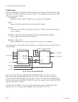
Overlaying the graphics on the video data is performed by the combination of the Graphics Overlay ASIC
(IC352) and 16 bit-SDRAM (IC353). (Refer to Fig. 3-14.) In the Graphics Overlay ASIC (IC352), the
graphics data that is written by the CPU overwrites on top of the video signal that is input from the
VCPex (IC300), and is output to the Video Encoder (IC402). The H sync signal, V sync signal and field
ID signals are input from the Video Encoder (IC402) to the Graphic Overlay ASIC (IC352). Creation of
the I
2
C bus signals that enables the CPU to control the Video Decoder (IC400) and Video Encoder
(IC402), and creation of the 27 MHz clock signal that is used in the VCP, VIDAD and VIDDA blocks are
performed by Graphics Overlay ASIC (IC352). In addition to the above, selection of the input S-video
signals, resetting the Pre-filter ASIC (IC350), Video Decoder (IC400) and Video Encoder (IC402) and
selection of microphone inputs are controlled by the output port signal of the Graphics Overlay ASIC
(IC352).
The operating clock (54 MHz) of the Graphics Overlay ASIC (IC352) is supplied from the crystal
oscillator X350. Resetting is performed by the “RES_STB” signal that is supplied from the CPU block.
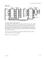
The Video Encoder (IC402) converts the video data that is input from the Graphics Overlay ASIC
(IC352) to the NTSC/PAL video signal. The input video data is the 8-bit data in which the luminance and
the chrominance signals are multiplexed. The operating clock signal (27 MHz) is obtained from the
output of the Graphics Overlay ASIC (IC352). The controls from the CPU are performed using the I
2
C
bus via the Graphics Overlay ASIC (IC352). Resetting is controlled by the output port of the Graphics
Overlay ASIC (IC352). (Refer to Fig. 3-15.) Power to the video output analog circuit is the
+
5 V-4
power that is obtained from the
+
5 V-2 power supply via an LC filter.
It operates on the
+
3.3 V-2 and the
+
5 V-2 power supply voltage.
[VIDIN block]
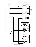
The VIDIN block is the analog video circuit up to the Video Decoder (IC400) that consists of 75
Z
terminating resistors, the Video Selector (IC401) and others. (Refer to Fig. 3-15.)
The S-video input signal including the luminance and chrominance signals, is selected either from the
camera or AUX-1 by the Video Selector (IC401). The selected signal is input to the Video Decoder
(IC400). The input signal selection is controlled by the output port of the Graphics Overlay ASIC
(IC352). The composite signal that is input from AUX-2 is input to the Video Decoder (IC400) via the
buffer circuit (Q406). The composite signal that is input from the AV-Link input (DE-54 board) is
directly input to the Video Decoder (IC400).
Power to the VIDIN block is the
+
5 V-3 power that is obtained from the
+
5 V-2 power supply via an LC filter.
[VIDOUT block]
The VIDOUT block is the analog video circuit up to the video output connector from the Video Encoder
(IC402) that consists of the low-pass filters (FL402 to FL404), the Video Drivers (IC403, IC404) and
others. (Refer to Fig. 3-15.)
The S-video luminance signal, chrominance signals and composite signal that are output from the Video
Encoder (IC402) are terminated by 200
Z
and are passed through the respective low-pass filters to
remove the unwanted high frequency components. The output video level is adjusted in accordance with
the PAL and NTSC broadcast formats by the circuit constants of the low-pass filter circuit. The low-pass
filter circuit operates on the
+
10 V power voltage.
The video signals that have passed through the low-pass filter enter the Video Drivers (IC403, IC404)
where they are amplified by 6 dB, and feed the output connector through a 75
Z
serial resistor. Power to
the Video Drivers (IC403, IC404) is the
+
5 V-4 power that is obtained from the
+
5 V-2 power supply via
an LC filter.
3-2. Circuit Description of the Respective Boards
Summary of Contents for PCS-1500
Page 8: ......
Page 75: ...1 67 PCS 1500 1500P Sony Corporation Printed in Japan ...
Page 76: ......
Page 130: ......
Page 198: ......


