background image

5-1

RDR-GX220/GX330

SECTION 5

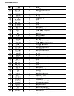
IC PIN FUNCTION DESCRIPTION

Pin No.

Pin name

I/O

Function

1

ONDO

I

Detection of board temperature

2

SIRCSIN

I

Input  of remote control signal

3

AVLINK-IN

I

Fixed at “L”

4

FLD_DATA

O

Output of FLD data signal

5

FLD_IN

I

Fixed at “L”

6

FLD_CLK

O

Output of FLD clock signal

7

BYTE

I

Fixed at “L”

8

CNVSS

I

Connected to GND when the flash is overwritten is VCC

9

XCIN

I

Input of sub-clock signal  (32.768KHz)

1 0

XCOUT

O

Not used

1 1

_RESET

I

Input of system reset signal input

1 2

XOUT

O

Output of main-clock signal (10MHz)

1 3

VSS

Digital GND

1 4

XIN

I

Input of main-clock signal (10MHz)

1 5

VCC1

Power supply input  (Analog 5V)

1 6

_NMI

I

Fixed at “H”

1 7

INT_RTC

I

Input of RTC INT signal from RTC

1 8

_IT_REQ

I

Input of communication request signal with system controller

1 9

SLICE

I

Input of slicer operation detection from 37 Pin

2 0

IT_XRST

O

Output communication reset signal with RISM 3

2 1

DIMMER

O

Output of LED power supply switch

2 2

JUST_CLK_2

O

Not used

2 3

RISM_STATUS2

O

Output of communication status 2 signal with system controller

2 4

P75

O

Not used

2 5

P74

O

Not used

2 6

P73

O

Not used

2 7

AVLINK-OUT

O

Not used

2 8

TU_SCL_1

O

Output of IIC clock signal

2 9

TU_SDA_1

O

Input/output IIC data signal

3 0

VSS2

Analog GND

3 1

LP2

O

Output of filter signal 2 (for Fsc)

3 2

LP3

O

Output of filter signal 3 (forVPS)

3 3

LP4

O

Output of filter signal 4 (for PDC)

3 4

VDD2

Power supply input (Analog 5V)

3 5

TEST1

Fixed at “L”

3 6

M 1

Fixed at “L”

3 7

SLICEON

O

Output of slicer operation detection (to 

ql

 pin)

3 8

IT_SOUT

O

Output of serial TXD 1 signal with system controller

3 9

IT_SIN

I

Input of serial RXD 1 signal with system controller

4 0

IT_SCLK

O

Output of serial CLK 1 signal with system controller

4 1

MONITOR

I

Input of RTS signal with system controller

4 2

TU_SDA_2

O

Not used

4 3

TU_SCL_2

O

Not used

4 4

RISM_STATUS3

O

Not used

4 5

RISM_STATUS1

I

Input of communication status 1 signal with system controller

4 6

CLKOUT

O

Analog GND

4 7

PCONT

O

Output of switch system power control signal

4 8

FAN_DET

I

Input of fan stopping detect signal

4 9

FAN_ONOFF

O

Output of fan on/off signal (“H”:fan on)

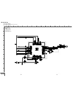
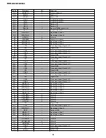
5-1. IT CONTROL IC (IC603: M306H5FGFP-C35FP/-C37FP) (AV-100 BOARD))

Summary of Contents for RDR-GX330 - DVD Recorder With TV Tuner

Page 1: ...jack 1 0 Vp p S VIDEO 4 pin mini DIN Y 1 0 Vp p C 0 286 Vp p NTSC GX330 0 3 Vp p PAL GX220 LINE 1 IN LINE 2 IN AUDIO Phono jack 2 Vrms more than 22 kilohms VIDEO Phono jack 1 0 Vp p S VIDEO 4 pin mini DIN Y 1 0 Vp p C 0 286 Vp p NTSC GX330 0 3 Vp p PAL GX220 DV IN 4 pin i LINK S100 DIGITAL OUT COAXIAL Phono jack 0 5 Vp p 75 ohms COMPONENT VIDEO OUT Y PB PR GX330 Y PB CB PR CR GX220 Phono jack Y 1 ...

Page 2: ... return to chassis must not exceed 0 5mA 500 microampers Leakage current can be measured by any one of three methods 1 A commercial leakage tester such as the Simpson 229 or RCA TW 540A Follow the manufacturers instructions to use these instruments 2 A battery operatedAC milliammeter The Data Precision 245 digital multimeter is suitable for this job 3 Measuring the voltage drop across a resistor b...

Page 3: ...esetting the Recorder 1 20 Additional Information 1 20 Troubleshooting 1 20 Self diagnosis Function When letters numbers appear in the display 1 21 Notes About This Recorder 1 21 Specifications 1 22 About i LINK 1 22 Guide to Parts and Controls 1 22 2 DISASSEMBLY 2 1 Upper Case 2 2 2 2 Tray Cover Assembly 2 2 2 3 Front Panel Section 2 3 2 4 FL 155 Board FR 237 Board 2 3 2 5 DVD Drive 2 4 2 6 RD 60...

Page 4: ...s and Description of Service Mode Menu 6 3 6 4 Device Check Menu Diagnostic Test 6 4 7 ELECTRICAL ADJUSTMENT 7 1 Video System Adjustment GX330 7 1 7 2 Video System Adjustment GX220 7 3 8 REPAIR PARTS LIST 8 1 Exploded Views 8 1 8 1 1 Overall Section 8 1 8 1 2 Chassis Section 8 2 8 2 Electrical Parts List 8 3 ...

Page 5: ...mes impossible Note2 If you close the tray with a CD disc inserted in it the CD can be ejected However if you close the tray while it is empty there can be a case that ejection of the tray becomes impossible Note3 Even if you replace the DVD drive unit while the tray remains under the state as described above the situation cannot be improved 2 If the tray cannot be ejected while the disc is not in...

Page 6: ...he Disc Information display Playable only on DVD R in VR mode compatible players finalisation necessary page 32 Video mode Automatically formatted in Video mode Playable on most DVD players finalisation necessary page 32 RW RWVR RWVideo R RVR RVideo continued 8 Usable disc versions as of March 2006 8x speed or slower DVD RWs 6x speed or slower DVD RWs Ver 1 1 Ver 1 2 with CPRM 2 16x speed or slowe...

Page 7: ...ome DVD RWs DVD Rs DVD RWs DVD Rs DVD RAMs or CD RWs CD Rs cannot be played on this recorder due to the recording quality or physical condition of the disc or the characteristics of the recording device and authoring software The disc will not play if it has not been correctly finalised For more information see the operating instructions for the recording device You cannot mix VR mode and Video mo...

Page 8: ...Inc Step 4 Connecting the AC Power Cord Mains Lead Connect the supplied AC power cord mains lead to the AC IN terminal of the recorder Then plug the recorder and TV power cords mains leads into the mains After you connect the AC power cord mains lead you must wait for a short while before operating the recorder You can operate the recorder once the front panel display lights up and the recorder en...

Page 9: ...D2 you will be unable to operate this recorder Changing programme positions of the recorder using the remote Number buttons ENTER 19 Hookups and Settings Step 6 Easy Setup Make the basic adjustments by following the on screen instructions in Easy Setup 1 Turn on the recorder and your TV Then switch the input selector on your TV so that the signal from the recorder appears on your TV screen The ini...

Page 10: ...lose the disc tray Wait until LOAD disappears from the front panel display Unused DVDs are formatted automatically For DVD RW discs DVD RWs are formatted in the recording format VR mode or Video mode set by Format DVD RW in the DVD setup For DVD R discs DVD Rs are automatically formatted in Video mode To format an unused DVD R in VR mode format the disc using the Disc Information display page 34 b...

Page 11: ...t scene of the recording title Order Sorted By Date In order of when the titles were recorded The title that is recorded most recently is listed at the top By Title In alphabetical order By Number In order of recorded title number Sub menu 27 Eight Basic Operations Getting to Know Your DVD Recorder 4 Displaying the Playing Remaining Time and Play Information You can check the playing time and rema...

Page 12: ...isc See 1 Inserting a Disc on page 23 2 Press OPTIONS to select Disc Information and press ENTER The Disc Information display appears Available settings differ depending on the disc type Example When the inserted disc is a DVD RW 3 Select Disc Name and press ENTER Enter the disc name in the Input Disc Name display page 29 b Note You can enter up to 64 characters for a DVD s disc name The disc name...

Page 13: ...whether or not the recorder is turned on You can turn off the recorder without affecting the recording even after recording starts b Note To play a recorded disc on other DVD equipment finalise the disc page 32 Like the standard 3 recording modes of video tapes you can select the desired recording mode using the REC MODE button Recording modes with higher quality provide a more beautiful recording...

Page 14: ...ge 43 Even if the timer is set for the same daily or weekly programme the timer recording cannot be made if it overlaps with a programme that has priority will appear next to the overlapped setting in the Timer List Check the priority order of the settings Even if the timer is set timer recordings cannot be made while recording a programme that has priority The Rec Mode Adjust function only works ...

Page 15: ...the overlapped setting in the Timer List Check the priority order of the settings will be cut off 43 Timer Recording Recording From Connected Equipment You can set the recorder to automatically record programmes from connected equipment that has a timer function such as a satellite tuner Connect the equipment to the LINE 1 IN jacks of the recorder page 22 When the connected equipment turns on the ...

Page 16: ... on the recorder you turn off the recorder VIDEO CD CD DATA DVD DATA CD only you make a recording except for DVD RWs DVD Rs in VR mode you disconnect the AC power cord mains lead To play restricted DVDs Parental Control If you play a restricted DVD the message Do you want to temporarily change the Parental Control level to appears on your TV screen 1 Select OK and press ENTER The display for enter...

Page 17: ...n if you fast forward the recorded programme there will always be a time difference of about one minute or more between the recorded programme and the current TV broadcast You can play a previously recorded programme while recording another on the same disc Playback continues even if the recording is a timer recording 1 While recording press TITLE LIST The Title List appears 2 Select the title you...

Page 18: ...yback may not be possible For example the picture may be unclear playback may not appear smooth the sound may skip and so on Depending on the disc playback may take some time to start Some files cannot be played Albums play in the following order Structure of disc contents When you insert a DATA CD DATA DVD and press H the numbered tracks or files are played sequentially from 1 through 7 For JPEG ...

Page 19: ...otes Images or sound may be momentarily interrupted at the point where you erase a section of a title Sections shorter than five seconds may not be erased For DVD RWs the erased section may be slightly different from the points you selected You can manually insert a chapter mark at any point you like during playback or recording Press CHAPTER MARK at the point where you want to divide the title in...

Page 20: ...the tape for you you do not need to operate your digital video camera Do the following to start using the DV Edit functions of this recorder See the instruction manual supplied with the digital video camera as well before connecting z Hint If you plan to do additional editing on a disc after the initial dub use the DV IN jack and record on a DVD RW DVD R VR mode b Notes You cannot make a recording...

Page 21: ...ER if the IN point is correct If the IN point is incorrect select the IN point using c C and press ENTER The display for setting the OUT point end of the scene appears 6 Select the OUT point using m M and press ENTER Playback pauses 7 Press ENTER if the OUT point is correct If the OUT point is incorrect select the OUT point using c C and press ENTER The selected scene is added to the scene informa...

Page 22: ...the programme position of another station repeat from step 2 Some broadcast systems provide a Teletext service in which complete programmes and their data title date programme position recording start time etc are stored day by day A TV guide page corresponds to each day of the week When recording a programme the recorder automatically takes the programme name from the Teletext pages and stores it...

Page 23: ...n DISPLAY is pressed On Turns on the screen saver function Off Turns off the function 75 Settings and Adjustments Audio Settings Audio The Audio setup allows you to adjust the sound according to the playback and connection conditions 1 Press SYSTEM MENU while the recorder is in stop mode 2 Select SETUP and press ENTER 3 Select Audio and press ENTER The Audio setup appears with the following option...

Page 24: ...assword appears enter a new four digit password using the number buttons then select OK and press ENTER b Notes If you forget your password you will have to reset it by selecting Parental Control of Factory Setup in the Others setup page 80 When you play discs which do not have the Parental Control function playback cannot be limited on this recorder Depending on the disc you may be asked to chang...

Page 25: ...screen even though the picture size is set in TV Type of the Video Output in the Video setup The picture size of the title is fixed There is no sound Re connect all connections securely The connecting cord is damaged The input source setting on the amplifier or the connection to the amplifier is incorrect The recorder is in reverse play fast forward slow motion or pause mode If the audio signal do...

Page 26: ...ricity etc causes the recorder to operate abnormally turn off the recorder and wait until the clock appears in the front panel display Then unplug the recorder and after leaving it off for a while plug it in again Five numbers or letters are displayed in the front panel display The self diagnosis function was activated see the table on page 87 The disc tray does not open after you press Z open clo...

Page 27: ...patible equipment having two or more i LINK jacks DV jacks see the instruction manual of the equipment to be connected i LINK is a more familiar term for IEEE 1394 data transport bus proposed by SONY and is a trademark approved by many corporations IEEE 1394 is an international standard standardized by the Institute of Electrical and Electronics Engineers i LINK s maximum baud rate varies accordin...

Page 28: ...ator 46 Displays DATA CDs as CD z Hint You can turn off the front panel display when the recorder is turned off by setting Dimmer to Save Power in the Others setup page 80 A AERIAL IN OUT jacks 11 B LINE 1 IN R AUDIO L VIDEO jacks 12 C LINE 1 IN S VIDEO jack 20 D DIGITAL OUT COAXIAL jack 14 E LINE OUT R AUDIO L VIDEO jacks 12 14 F AC IN terminal 15 G LINE OUT S VIDEO jack 12 H COMPONENT VIDEO OUT ...

Page 29: ... disassembly procedure SECTION 2 DISASSEMBLY Set Upper case Page 2 2 FL 155 board FR 237 board Page 2 3 Tray cover assembly Page 2 2 Front panel section Page 2 3 DVD drive Page 2 4 RD 60 board Page 2 4 D C fan Page 2 6 AV 100 board Page 2 5 Power block Page 2 6 ...

Page 30: ... 2 2 TRAY COVER ASSEMBLY Note Follow the disassembly procedure in the numerical order given 1 Two tapping screws 3 Upper case 2 Three tapping screws BV3 3 CR 3 x 8 1 The stiff wire Hole 4 Tray cover assembly 3 Two claws 2 Open the tray ...

Page 31: ...ble flat cable FAR 003 CN3002 3 Flexible flat cable FAR 002 CN3005 8 Three tapping screws BV3 3 CR 3 x 8 4 Two Non HALOGENE tapes 6 Tapping screw BV3 3 CR 3 x 8 5 Flexible flat cable FLR 006 q Remove the FR 237 board in the direction of the arrow 2 Non HALOGENE tape 9 Harness RF 117 CN3004 7 Remove the FL 155 board in the direction of the arrow ...

Page 32: ... 3 x 10 1 Flexible flat cable FRD 010 CN101 5 Two Non HALOGENE tapes 8 DVD drive 6 Flexible flat cable FRD 010 2 6 RD 60 BOARD 2 Flexible flat cable FRA 005 CN603 3 Flexible flat cable FRA 003 CN604 4 Flexible flat cable FRD 010 CN101 1 Connector CN601 6 Four tapping screws BV3 3 CR 3 x 8 8 RD 60 board 5 Harness Connector RF 117 CN701 7 Harness PD 137 ...

Page 33: ...d Remove the AV 100 board in the direction of the arrow qs Three tapping screws BV 3 x 8 q Screw B3 3 CR 3 x 8 6 Connector CN3 7 Connector CN601 2 Connector CN103 1 The wire pin that holds the harness is set up 3 The wire pin that holds the flexible flat cables are set up qa Five tapping screws BV3 3 CR 3 x 10 5 Flexible flat cable FAR 003 CN602 ...

Page 34: ...rews BV3 3 CR 3 x 8 1 Connector CN3 2 Tapping screw P 3 x 8 4 Remove the Power block in the direction of the arrow 3 Two tapping screws BV3 3 CR 3 x 10 4 Remove the D C fan in the direction of the arrow 2 Connector CN103 1 The wire pin that holds the harness is set up ...

Page 35: ...r block RD 60 board FR 237RISM3 TA_SATA CN V DEC DTT IF Flash ROM OPTION CN AV_CN POWER DV PHY PLL AUDIO_AD_DA AV 100 board POWER AUDIO IN AUDIO OUT TUNER IT CONTROLLER VIDEO IN OUT FL 155 board POWER SWITCH FR 237 board FL DRIVE LINE2 IN FUNCTION SW 2 7E ...

Page 36: ...IO ADC DAC IC803 VIDEO AMP SELECTOR IC702 REMOTE COMMANDER RECEIVER IC3002 AUDIO IN SELECT IC201 IC1401 Y2 TUL TUR MONO IN OUT L OUT R SIRCS KEY0 KEY1 FR 5V XPAMUTE Y C C2 V2 L2 R2 L1 R1 Y1 C1 V1 FR 237 BOARD 1 3 AV 100 BOARD J702 LINE 1 IN S VIDEO VIDEO AUDIO R AUDIO L Y C Y C 6 IC103 RISM3 MUTING COMPONENT VIDEO OUT FUNCTION KEY UNSW4V OUT RESET IC606 AND GATE IC605 SUPER AND MEMORY 128Mbit IC50...

Page 37: ...INSEL_2 INSEL_1 12 14 2 R2 IN TU R L1 L2 IN TU L 9 10 13 3 VIDEO AMP SELECTOR IC702 5 R1 EQ IC202 AUDIO IN SELECT IC201 IC1401 AMP IC203 Y G G C Y C J701 J701 LINE OUT DIGITAL OUT COAXIAL S VIDEO VIDEO AUDIO R AUDIO L Y CB CR COMPONENT VIDEO OUT 13 11 9 7 5 3 1 14 21 20 18 17 27 26 24 23 13 12 11 10 9 8 7 6 3 2 XL MUTE 2 1 MUTING Q309 310 D301 D303 AUDIO AMPLIFIER IC302 TO FROM RD 060 BOARD CN603 ...

Page 38: ...26 27 16 51 20 47 21 22 23 24 45 46 DQ0 DQ15 A0 XWE XCAS XRAS CS CK XCK A12 BA0 1 LDQS UDQS LDM UDM 2 4 5 7 54 56 57 59 8 10 11 13 60 62 63 65 26 27 16 51 20 47 21 22 23 24 45 46 DQ0 DQ15 A0 XWE XCAS XRAS CS CK XCK A12 BA0 1 LDSS UDQ3 LDM UDM H7 H10 F7 G6 8 10 E10 E7 D7 9 10 J3 K3 K10 E4 K9 E3 F4 I O1 I O16 NAND CS HADRS 19 HADRS 20 INT 2 HOE HWS 0 ALE CE CLE R R RE WE DSE 35 42 44 51 54 56 31 1 1...

Page 39: ...VER IC3001 FLD LED DRIVER IC702 VIDE0 AMP SELECTOR IC701 3 3V REG IC604 AND GATE CN601 Q601 605 VIDEO BUFFER Q606 Q607 BUFFER D503 FR 5V CN3001 KEY0 KEY0 FL POW 6V CN3002 2 10 1 7 9 3 4 6 5 D1301 1304 T3001 DC DC CONVERTER TRANSFORMER S3101 CN31O1 F2 F1 ND3001 FLUORESCENT INDICATOR TUBE Q3001 3002 OSC POWER IC202 203 EQ IC302 AUDIO AMP IC303 5V REG IC402 5V REG IC104 5V REG IC102 3 3V REG IC107 FA...

Page 40: ...E_A0 IDE_D9 IDE_A3 CS1 GND GND IDE_RST IDE_D14 IDE_D0 GND GND GND IDE_R IDE_D8 IDE_D1 IDE_INT IDE_D12 IDE_D7 IDE_D2 N C IDE_D4 IDE_D13 IDE_D5 GND IDE_A1 IDE_DREQ N C IDE_HD16 IDE_D3 IDE_A4 CS0 IDE_D11 IDE_IORDY IDE_W AV 100 RD 060 DGND TPB TPB TPA TPA DGND FR 237 UNSW 8V GND GND UNSW4V PCONT UNSW12V SW5V GND UNSW6V UNSW6V FL 155 POWER Fan DVD DRIVE FLR 006 FFC 1 0mm l 211 5 FAR 002 FFC 1 0mm l 335...

Page 41: ...ignal on DVD refer ence disc and when playing CD reference disc Readings are taken with a digital multimeter DC 10MΩ Voltage variations may be noted due to normal production tolerances 4 2 SCHEMATIC DIAGRAMS THIS NOTE IS COMMON FOR SCHEMATIC DIAGRAMS In addition to this the necessary note is printed in each block WAVEFORMS AV 100 BOARD 4 3 4 4 WAVEFORMS AV 100 RD60 When indicating parts by referen...

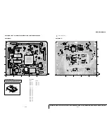
Page 42: ...ounted in this model For printed wiring board 4 5 POWER AUDIO IN AUDIO OUT TUNER IT CONTROLLER VIDEO IN OUT AV 100 AV 100 SIDE A AV 100 SIDE B Power block RD 60 board FR 237RISM3 TA_SATA CN V DEC DTT IF Flash ROM OPTION CN AV_CN POWER DV PHY PLL AUDIO_AD_DA AV 100 board POWER AUDIO IN AUDIO OUT TUNER IT CONTROLLER VIDEO IN OUT FL 155 board POWER SWITCH FR 237 board FL DRIVE LINE2 IN FUNCTION SW SI...

Page 43: ...for printed wiring board of AV 100 board Refer to page 4 4 for waveform AV 100 1 6 BOARD POWER REF NO 1000 SERIES XX MARK NO MOUNT NO MARK PB MODE MARKED MOUNT TABLE 4 7 4 8 POWER AV 100 1 6 The components identified by mark or dotted line with mark are critical for safety Replace only with part number specified ...

Page 44: ...8 7 6 5 4 3 14 15 AV 100 2 6 BOARD AUDIO IN REF NO 1000 SERIES XX MARK NO MOUNT NO MARK PB MODE MARKED MOUNT TABLE 4 9 4 10 AUDIO IN AV 100 2 6 For Schematic Diagram Refer to page 4 5 for printed wiring board of AV 100 board Refer to page 4 4 for waveform ...

Page 45: ... 7 6 5 4 3 14 15 AV 100 3 6 BOARD AUDIO OUT REF NO 1000 SERIES XX MARK NO MOUNT NO MARK PB MODE MARKED MOUNT TABLE 4 11 4 12 AUDIO OUT AV 100 3 6 For Schematic Diagram Refer to page 4 5 for printed wiring board of AV 100 board Refer to page 4 4 for waveform ...

Page 46: ... 6 5 4 3 14 15 AV 100 4 6 BOARD TUNER REF NO 1000 SERIES XX MARK NO MOUNT NO MARK PB MODE MARKED MOUNT TABLE 4 13 4 14 TUNER AV 100 4 6 For Schematic Diagram Refer to page 4 5 for printed wiring board of AV 100 board Refer to page 4 4 for waveform 9 RDR GX330 ...

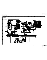
Page 47: ... XX MARK NO MOUNT NO MARK PB MODE MARKED MOUNT TABLE 4 15 4 16 IT CONTROLLER AV 100 5 6 For Schematic Diagram Refer to page 4 5 for printed wiring board of AV 100 board Refer to page 4 4 for waveform The components identified by mark or dotted line with mark are critical for safety Replace only with part number specified ...

Page 48: ...5 4 3 14 15 AV 100 6 6 BOARD VIDEO IN OUT REF NO 1000 SERIES XX MARK NO MOUNT NO MARK PB MODE MARKED MOUNT TABLE 4 17 4 18 VIDEO IN OUT AV 100 6 6 For Schematic Diagram Refer to page 4 5 for printed wiring board of AV 100 board Refer to page 4 4 for waveform REC ...

Page 49: ...19 for printed wiring board of FL 155 board FL 155 BOARD POWER SWITCH REF NO 1000 SERIES XX MARK NO MOUNT NO MARK REC PB MODE FL 155 BOARD SIDE B A B 1 FL 155 BOARD SIDE A A B 1 1 A B C D E F G 2 7 6 5 4 3 Power block RD 60 board FR 237RISM3 TA_SATA CN V DEC DTT IF Flash ROM OPTION CN AV_CN POWER DV PHY PLL AUDIO_AD_DA AV 100 board POWER AUDIO IN AUDIO OUT TUNER IT CONTROLLER VIDEO IN OUT FL 155 b...

Page 50: ...L DRIVE LINE2 IN FUNCTION SW PRINTEDWIRING BOARD Uses unleaded solder There are a few cases that the part printed on this diagram isn t mounted in this model For printed wiring board 4 21 FL DRIVE LINE2 IN FUNCTION SW FR 237 FR 237 SIDE A FR 237 BOARD SIDE B Power block RD 60 board FR 237RISM3 TA_SATA CN V DEC DTT IF Flash ROM OPTION CN AV_CN POWER DV PHY PLL AUDIO_AD_DA AV 100 board POWER AUDIO I...

Page 51: ...7 6 5 4 3 14 15 For Schematic Diagram Refer to page 4 21 for printed wiring board of FR 237 board FR 237 BOARD FL DRIVE LINE2 IN FUNCTION SW REF NO 1000 SERIES XX MARK NO MOUNT NO MARK PB MODE MARKED MOUNT TABLE 4 23 4 24 FL DRIVE LINE2 IN FUNCTION SW FR 237 ...

Page 52: ...E6 C1 H1 F1 Y1 L1 J1 AA1 W1 W3 G3 AC3 M3 D3 E3 P3 U3 R3 V3 AD1 AB1 K1 N1 T1 B1 A1 AE1 AD3 AB3 K3 AA13 AA15 AA11 AA19 AA14 AA10 AA16 AA12 AA7 AA8 AA9 AA6 Y21 L21 J21 W21 G21 K21 N21 T21 H21 F21 P21 U21 R21 V21 M21 1 4 5 8 9 1 5 10 15 20 25 30 66 33 34 40 45 50 55 60 1 5 10 15 20 25 30 66 33 34 40 45 50 55 60 1 4 5 8 1 4 5 8 9 1 2 3 4 5 7 2 3 1 5 4 6 G7 H7 J7 K7 F7 E7 D7 C7 G8 H8 J8 K8 F8 E8 D8 C8 G...

Page 53: ... RISM3 REF NO 1000 SERIES XX MARK NO MOUNT NO MARK PB MODE MARKED MOUNT TABLE For Schematic Diagram Refer to page 4 25 for printed wiring board of RD 60 board Refer to page 4 4 for waveform RISM3 RD 60 1 8 SIGNAL PATH VIDEO SIGNAL CHROMA REC PB Y Y CHROMA AUDIO SIGNAL TO DISK DRIVE CN202 PAGE 4 59 ...

Page 54: ...7 6 5 4 3 14 15 4 30 4 29 RD 60 2 8 BOARD ATA_SATA CN REF NO 1000 SERIES XX MARK NO MOUNT NO MARK PB MODE MARKED MOUNT TABLE For Schematic Diagram Refer to page 4 25 for printed wiring board of RD 60 board Refer to page 4 4 for waveform ATA_SATA CN RD 60 2 8 ...

Page 55: ...0 9 8 7 6 5 4 3 14 15 4 31 4 32 RD 60 3 8 BOARD V DEC REF NO 1000 SERIES XX MARK NO MOUNT NO MARK PB MODE MARKED MOUNT TABLE For Schematic Diagram Refer to page 4 25 for printed wiring board of RD 60 board Refer to page 4 4 for waveform V DEC RD 60 3 8 ...

Page 56: ... 9 8 7 6 5 4 3 14 15 4 34 4 33 RD 60 4 8 BOARD DTT IF REF NO 1000 SERIES XX MARK NO MOUNT NO MARK PB MODE MARKED MOUNT TABLE For Schematic Diagram Refer to page 4 25 for printed wiring board of RD 60 board Refer to page 4 4 for waveform DTT IF RD 60 4 8 ...

Page 57: ... ROM OPTION CN REF NO 1000 SERIES XX MARK NO MOUNT NO MARK PB MODE MARKED MOUNT TABLE For Schematic Diagram Refer to page 4 25 for printed wiring board of RD 60 board Refer to page 4 4 for waveform Flash ROM OPTION CN RD 60 5 8 RISM3 P1 RISM3 P1 FLASH MEMORY P5 FLASH MEMORY P5 RISM3 P1 RISM3 P1 RISM3 P1 ...

Page 58: ...7 6 5 4 3 14 15 4 38 4 37 RD 60 6 8 BOARD AV_CN POWER REF NO 1000 SERIES XX MARK NO MOUNT NO MARK PB MODE MARKED MOUNT TABLE For Schematic Diagram Refer to page 4 25 for printed wiring board of RD 60 board Refer to page 4 4 for waveform AV_CN POWER RD 60 6 8 ...

Page 59: ... 9 8 7 6 5 4 3 14 15 4 39 4 40 RD 60 7 8 BOARD DV PHY REF NO 1000 SERIES XX MARK NO MOUNT NO MARK PB MODE MARKED MOUNT TABLE For Schematic Diagram Refer to page 4 25 for printed wiring board of RD 60 board Refer to page 4 4 for waveform DV PHY RD 60 7 8 ...

Page 60: ...5 4 3 14 15 4 42 4 41 RD 60 8 8 BOARD PLL AUDIO_AD_DA REF NO 1000 SERIES XX MARK NO MOUNT NO MARK PB MODE MARKED MOUNT TABLE For Schematic Diagram Refer to page 4 25 for printed wiring board of RD 60 board Refer to page 4 4 for waveform PLL AUDIO_AD_DA RD 60 8 8 ...

Page 61: ...1 C 5 D502 C 6 D601 C 5 D602 C 6 SIDE B D101 A 6 There are a few cases that the part printed on this diagram isn t mounted in this model For printed wiring board A B C D 1 2 5 4 3 7 6 A B C D 1 2 5 4 3 7 6 POWER BOARD POWER BLOCK SRV1855EK Power block RD 60 board FR 237RISM3 TA_SATA CN V DEC DTT IF Flash ROM OPTION CN AV_CN POWER DV PHY PLL AUDIO_AD_DA AV 100 board POWER AUDIO IN AUDIO OUT TUNER I...

Page 62: ...critical for safety Replace only with part number specified 4 45 4 46 For Schematic Diagram Refer to page 4 43 for printed wiring board of Power board POWER BOARD POWER SUPPLY SRV1855EK GX220 REF NO 1000 SERIES XX MARK NO MOUNT NO MARK PB MODE MARKED MOUNT TABLE POWER BOARD POWER BLOCK SRV1855EK TO DRIVE TO AV 100 BOARD CN104 PAGE 4 7 ...

Page 63: ...1 C 5 D502 C 6 D601 C 5 D602 C 6 SIDE B D101 A 6 There are a few cases that the part printed on this diagram isn t mounted in this model For printed wiring board A B C D 1 2 5 4 3 7 6 A B C D 1 2 5 4 3 7 6 POWER BOARD POWER BLOCK SRV1856WW Power block RD 60 board FR 237RISM3 TA_SATA CN V DEC DTT IF Flash ROM OPTION CN AV_CN POWER DV PHY PLL AUDIO_AD_DA AV 100 board POWER AUDIO IN AUDIO OUT TUNER I...

Page 64: ...critical for safety Replace only with part number specified 4 49 4 50E For Schematic Diagram Refer to page 4 41 for printed wiring board of Power board POWER BOARD POWER SUPPLY SRV1856WW GX330 REF NO 1000 SERIES XX MARK NO MOUNT NO MARK PB MODE MARKED MOUNT TABLE POWER BOARD POWER BLOCK SRV1856WW TO DRIVE TO AV 100 BOARD CN104 PAGE 4 7 ...

Page 65: ... RISM_STATUS2 O Output of communication status 2 signal with system controller 24 P75 O Not used 25 P74 O Not used 26 P73 O Not used 27 AVLINK OUT O Not used 28 TU_SCL_1 O Output of IIC clock signal 29 TU_SDA_1 O Input output IIC data signal 30 VSS2 Analog GND 31 LP2 O Output of filter signal 2 for Fsc 32 LP3 O Output of filter signal 3 forVPS 33 LP4 O Output of filter signal 4 for PDC 34 VDD2 Pow...

Page 66: ... Not used 71 VSS Digital GND 72 INSEL5 O Not used 73 BS_BIT_SW O Not used 74 BS_BST_CONT O Not used 75 BS_COR_DET O Not used 76 BS_CONV_CONT O Not used 77 BS_DEC_SW O Not used 78 BS_PCONT O Not used 79 BS_VOL_DET O Not used 80 SYNC_V_1 I Input of vertical synchronous signal 81 SYNC_V_2 I Fixed at L 82 NC I Not used 83 TU_PCONT_1 O Output of tuner power supply control signal H Power on 84 AUTO_PRES...

Page 67: ...og 5V 107 TEST3_CONT O Not used 108 START I Fixed at H 109 SYNCIN I Input composite video signal 110 SVREF I When slice the vertical synchronous signal input slice power 111 TEST2 I Fixed at GND 112 VDD3 Power supply input Analog 5V 113 CVIN1 I Input of component video signal 114 VSS3 Analog GND 115 TEST3 I Fixed at L 116 TU_AFT1 I Input of tuner ATF control signal ...

Page 68: ...TS 0 UART CSIO GPIO A25 DVDD Power supply input Digital 1 0V AA1 TRDATA 1 O Not used AA2 TRDATA 3 O Not used AA3 TRSYNC O Not used AA4 EVENT 0 O Not used AA5 VDD33 Power supply input Digital 3 4V AA6 VRMA Fixed at L AA7 VRMB Fixed at L AA8 VSSDAD10 Analog GND AA9 RREF1 REXT1 Fixed at L AA10 REF2 REXT2 Fixed at L AA11 VDD33 Power supply input Digital 3 4V AA12 VDD Power supply input Digital 1 0V AA...

Page 69: ...25 DDATA 2 Input output of data 2 AC1 TRDATA 5 O Not used AC2 TCK I Not used AC3 TDO O Not used AC4 VRPA Fixed at L AC5 VRPB Fixed at L AC6 VSSAAD10B Analog GND AC7 VCCDAD10 Power supply input Digital 3 3V ADC AC8 VSSDDA10A Digital GND AC9 VDDDDA10 Power supply input Digital 1 0V AC10 VSSDDA10B Fixed at L AC11 TESTMOD 1 O Fixed at L AC12 TESTMOD 6 O Fixed at L AC13 REC656H I Not used AC14 REC656I ...

Page 70: ... C AE6 VSSAAD10B Analog GND AE7 GOUT PD1 O Output of analog video signal G AE8 VSSADA10 Analog GND DAC AE9 YOUT PD4 O Output of analog video signal Y AE10 TESTMOD 0 O Fixed at L AE11 TESTMOD 3 O Fixed at L AE12 TESTMOD 4 O Fixed at L AE13 RESET I Input of hardware reset signal AE14 REC656I 0 I Not used AE15 R656CLKI I Not used AE16 REC656I 3 I Not used AE17 REC656I 5 I Not used AE18 REC656I 6 I No...

Page 71: ...O 0 C9 HCS 0 O Output of chip select signal 0 C10 HCS 5 Output of chip select signal GPIO 5 C11 HADRS 28 O Output of address 28 C12 HADRS 24 O Output of address 24 C13 HADRS 19 O Output of address 19 C14 HADRS 15 O Output of address 15 C15 HADRS 11 O Output of address 11 C16 HADRS 6 O Output of address 6 C17 MSDATA 1 Fixed at L C18 CTS 3 Not used C19 SCLK 1 UART CSIO GPIO C20 CTS 0 UART CSIO GPIO ...

Page 72: ...3 3V E13 VDD Power supply input Digital 1 0V E14 VSS Digital GND E15 VDD Power supply input Digital 1 0V E16 VSS Digital GND E17 VDD33 Power supply input Digital 3 3V E18 VDD Power supply input Digital 1 0V E19 VSS Digital GND E20 VDD Power supply input Digital 1 0V E21 VDD33 Power supply input Digital 3 3V E22 HDATA 4 Input output of data 4 E22 HDATA 14 Input output of data 14 E23 HDATA 12 Input ...

Page 73: ...3V J22 INT 8 Not used J23 DBI I SDI ICE JTAG TRST J24 INT 6 Fixed at H J25 INT 5 Fixed at H K1 AT2DATA 4 Fixed at L K2 AT2DATA 11 Fixed at L K3 AT2DATA 3 Fixed at L K4 AT2DATA 12 Fixed at L K5 VDD Power supply input Digital 1 0V K21 VSS Digital GND K22 INT4 Fixed at H K23 WP INT3 Fixed at H K24 SDA 1 Fixed at H K25 SDA 0 Fixed at H L1 AT2DATA 6 Fixed at L L2 AT2DATA 9 Fixed at L L3 AT2DATA 5 Fixed...

Page 74: ...25 DDATA 23 Input output of data 23 P1 ADCCLKI O Not used P2 LRCKO O Output of audio L R clock signal P3 A0DATAI I Input of audio signal P4 A0BCKI I Input of audio bit clock signal P5 VDD Power supply input Digital 3 3V P11 VSS Digital GND P12 VSS Digital GND P13 VSS Digital GND P14 VSS Digital GND P15 VSS Digital GND P21 DDATA 18 Input output of data 18 P22 DDATA 26 Input output of data 26 P23 DD...

Page 75: ...data strobe signal 2 V1 PHYDIO 5 Not used V2 PHYDIO 3 Not used V3 PHYDIO 0 Not used V4 PHYCTL 1 Not used V5 VDD33 Power supply input Analog 3 3V DAC V21 VDD Power supply input Digital 1 0V V22 VDD25 Power supply input Digital 2 5V V23 DDATA 15 Input output of data 15 V24 DDATA 7 Input output of data 7 V25 DDQS 0 Output of data strobe signal 0 W1 PHYDIO 2 Not used W2 PHYLPS O Not used W3 PHYSCLK I ...

Page 76: ...ars on the display panel of the main unit While the diagnostics is in progress either OK or NG appears on the monitor screen to enable the judgment whether the respective devices or the peripheral are normal or have any abnormality When an abnormality is detected the diagnostics is stopped at that moment and you can select to keep running the diagnostics or to stop it 6 1 Check Item When NG is dis...

Page 77: ...ed MAIN MENU 1 Version No 2 Display Color 3 Total Time 9 HDD MODE 0 G Code Setting MODEL SYSCON Version HDD Serial ID HDD Sony ID MAIN MENU Version No MODEL MRX151xxx Region Code SYSCON Version ITcon Version Drive Version Display Color 1 White Signal ON 2 White Signal OFF RETURN RETURN RETURN 2 1 RETURN 3 RETURN 4 RETURN 5 RETURN 6 RETURN 7 RETURN 8 RETURN 9 Total Time 1 Total Power ON 2 Total DVD...

Page 78: ...nu Diagnostic Test 1 Key 1 is not used 2 When the key 2 is pressed down the Super AND device check will be executed The SuperAND device is checked whether it is mounted or not and the I2C communication between Rism3 IC103 and Super AND is checked 3 Key 3 is not used 4 When the key 4 is pressed down the DDR Data device check willbeexecuted TheDDRdeviceischeckedwhetheritismounted or not and the elec...

Page 79: ...ification 1 0 V 0 07 p p Check method 1 Insert the NTSC reference disc and play back the 100 color bars 2 Confirm that the video level is 1 0 V 0 07 Vp p Fig 7 1 2 S Video Output S Y Check Purpose This check confirms that the S video Y signal output has the rated amplitude If it adjusted incorrectly the playback video signal will not be displayed corrected even when the S video cable is connected ...

Page 80: ...7 Vp p Fig 7 4 286 30mVp p 1 0 0 07Vp p 5 ComponentVideo Output B Y Check Purpose This check confirms that the B Y signal of the component video conforms to the NTSC standard If this signal level is not correct color of the video signal will have different color when the COMPONENT connector output signal is connected to a projector having COMPONENT input Mode PLAY Signal Color bars Test point COMP...

Page 81: ...e PAL reference disc and play back the 100 color bars 2 Confirm that the video level is 1 0 V 0 07 Vp p Fig 7 1 2 S Video Output S Y Check Purpose This check confirms that the S video Y signal output has the rated amplitude If it adjusted incorrectly the playback video signal will not be displayed corrected even when the S video cable is connected Mode PLAY Signal Color bars Test point S VIDEO OUT...

Page 82: ... 0 07 Vp p Fig 7 4 300 30mVp p 1 0 0 07Vp p 5 ComponentVideo Output B Y Check Purpose This check confirms that the B Y signal of the component video conforms to the PAL standard If this signal level is not correct color of the video signal will have different color when the COMPONENT connector output signal is connected to a projector having COMPONENT input Mode PLAY Signal Color bars Test point D...

Page 83: ...line with mark are critical for safety Replace only with part number specified RDR GX220 GX330 8 1 1 OVERALL SECTION 6 7 not supplied not supplied not supplied Chassis section 4 4 2 8 5 2 2 3 1 2 Ref No Part No Description Remark 1 X 2109 539 1 PANEL ASSY FRONT GX220 RUS 1 X 2109 538 1 PANEL ASSY FRONT GX220 AUS SP 1 X 2109 537 1 PANEL ASSY FRONT GX330 E 1 A 1206 211 A PANEL ASSY FRONT GX330 BR 2 ...

Page 84: ... FLAT FRA 005 54 1 831 410 11 CABLE FLEXIBLE FLAT FRA 003 55 1 468 959 21 POWER BLOCK GX220 55 1 468 960 11 POWER BLOCK GX330 Ref No Part No Description Remark Note The components identified by mark or dotted line with mark are critical for safety Replace only with part number specified 56 X 2109 036 1 COVER ASSY TRAY EXCEPT GX330 BR 56 A 1206 210 A COVER ASSY TRAY GX330 BR 57 1 797 413 11 DRIVE D...

Page 85: ...F 0 25PF 50V GX220 C1406 1 107 826 91 CERAMICCHIP 0 1UF 10 00 16V GX220 C1407 1 162 924 91 CERAMICCHIP 56PF 5 00 50V GX220 C1408 1 165 908 91 CERAMICCHIP 1UF 10 10V GX220 C1409 1 107 826 91 CERAMICCHIP 0 1UF 10 00 16V GX220 C1410 1 126 964 91 ELECT 10UF 20 00 50V GX220 C1411 1 126 962 91 ELECT 3 3UF 20 00 50V GX220 C1412 1 107 826 91 CERAMICCHIP 0 1UF 10 00 16V GX220 C1413 1 107 826 91 CERAMICCHIP...

Page 86: ...C628 1 125 891 11 CERAMICCHIP 0 47UF 10 00 10V C629 1 107 826 11 CERAMICCHIP 0 1UF 10 00 16V C630 1 125 891 11 CERAMICCHIP 0 47UF 10 00 10V C631 1 162 964 11 CERAMICCHIP 0 001UF 10 00 50V C632 1 107 826 11 CERAMICCHIP 0 1UF 10 00 16V C633 1 107 826 11 CERAMICCHIP 0 1UF 10 00 16V C634 1 107 826 11 CERAMICCHIP 0 1UF 10 00 16V C635 1 107 826 11 CERAMICCHIP 0 1UF 10 00 16V C639 1 107 826 11 CERAMICCHI...

Page 87: ...9 067 40 DIODESTZ6 8N T146 D731 8 719 067 40 DIODESTZ6 8N T146 D732 8 719 067 40 DIODESTZ6 8N T146 FERRITE FB201 1 414 228 11 FERRITE 0UH GX220 RUS FB202 1 414 228 11 FERRITE 0UH GX220 RUS FB301 1 414 228 11 FERRITE 0UH GX220 RUS FB302 1 414 228 11 FERRITE 0UH GX220 RUS FB701 1 500 283 11 FERRITE 0UH GX220 RUS FB702 1 500 283 11 FERRITE 0UH GX220 RUS FB703 1 500 283 11 FERRITE 0UH GX220 RUS FB704 ...

Page 88: ... R1410 1 216 825 91 METAL CHIP 2 2K 5 1 10W GX220 R1411 1 216 825 91 METAL CHIP 2 2K 5 1 10W GX220 R1412 1 216 846 91 METAL CHIP 120K 5 1 10W GX220 R1415 1 216 825 91 METAL CHIP 2 2K 5 1 10W GX220 R1416 1 216 864 11 SHORTCHIP 0 R142 1 216 295 91 SHORTCHIP 0 R144 1 216 295 91 SHORTCHIP 0 R145 1 216 295 91 SHORTCHIP 0 R1451 1 216 821 91 METAL CHIP 1K 5 1 10W R1452 1 218 895 91 METAL CHIP 100K 0 5 1 ...

Page 89: ...20 5 1 10W R350 1 211 989 91 METAL CHIP 68 5 1 10W R352 1 216 817 91 METAL CHIP 470 5 1 10W R354 1 216 817 91 METAL CHIP 470 5 1 10W R362 1 216 829 11 METAL CHIP 4 7K 5 1 10W R364 1 216 845 91 METAL CHIP 100K 5 1 10W R365 1 216 839 91 METAL CHIP 33K 5 1 10W R366 1 216 821 91 METAL CHIP 1K 5 1 10W R367 1 216 864 11 SHORTCHIP 0 EXCEPTGX220 RUS R368 1 216 864 11 SHORTCHIP 0 EXCEPTGX220 RUS R401 1 216...

Page 90: ...218 871 11 METAL CHIP 10K 0 5 1 10W R714 1 216 855 91 METAL CHIP 680K 5 1 10W R715 1 216 841 91 METAL CHIP 47K 5 1 10W R716 1 216 845 91 METAL CHIP 100K 5 1 10W R718 1 218 867 11 METAL CHIP 6 8K 0 5 1 10W R719 1 218 852 11 METAL CHIP 1 6K 0 5 1 10W R726 1 216 817 91 METAL CHIP 470 5 1 10W R728 1 216 840 91 METAL CHIP 39K 5 1 10W R729 1 216 837 91 METAL CHIP 22K 5 1 10W R733 1 216 864 11 SHORTCHIP ...

Page 91: ...ODESLI 343URT32WST FERRITE FB3006 1 414 228 11 FERRITE 0UH GX220 RUS FB3007 1 414 228 11 FERRITE 0UH GX220 RUS IC IC3001 8 759 643 83 ICUPD16315GB 3BS IC3002 6 600 500 01 ICGP1UM28XK0SF INDUCTOR L3001 1 412 537 31 INDUCTOR 100UH INDICATOR ND3001 1 519 849 21 INDICATORTUBE FLUORESCENT TRANSISTOR Q3001 8 729 901 88 TRANSISTOR2SC2411K T 146 CR Q3002 8 729 901 88 TRANSISTOR2SC2411K T 146 CR Q3003 6 55...

Page 92: ...124 1 165 908 91 CERAMICCHIP 1UF 10 10V C125 1 128 994 21 ELECT CHIP 47UF 20 10V C126 1 126 209 11 ELECT CHIP 100UF 20 00 4V C127 1 128 994 21 ELECT CHIP 47UF 20 10V C128 1 125 777 11 CERAMICCHIP 0 1UF 10 00 10V C129 1 125 777 11 CERAMICCHIP 0 1UF 10 00 10V C130 1 125 777 11 CERAMICCHIP 0 1UF 10 00 10V C131 1 125 777 11 CERAMICCHIP 0 1UF 10 00 10V C132 1 125 777 11 CERAMICCHIP 0 1UF 10 00 10V C133...

Page 93: ...20 RUS SP C336 1 125 777 11 CERAMICCHIP 0 1UF 10 00 10V GX220 RUS SP C337 1 125 777 11 CERAMICCHIP 0 1UF 10 00 10V GX220 RUS SP C338 1 125 777 11 CERAMICCHIP 0 1UF 10 00 10V GX220 RUS SP C339 1 164 943 81 CERAMICCHIP 0 01UF 10 00 16V GX220 RUS SP C340 1 164 943 81 CERAMICCHIP 0 01UF 10 00 16V GX220 RUS SP C501 1 137 710 91 CERAMICCHIP 10UF 20 6 3V C502 1 125 777 11 CERAMICCHIP 0 1UF 10 00 10V C504...

Page 94: ... 10UH GX220 RUS SP L302 1 469 555 21 INDUCTOR 10UH GX220 RUS SP L303 1 469 555 21 INDUCTOR 10UH GX220 RUS SP L601 1 419 630 21 COIL CHOKE 4 7UH L602 1 400 073 21 INDUCTOR 4 7UH L603 1 469 555 21 INDUCTOR 10UH GX220 RUS SP LF701 1 400 476 11 INDUCTOR 0UH TRANSISTOR Q601 8 729 010 05 TRANSISTORMSB709 RT1 Q602 8 729 010 05 TRANSISTORMSB709 RT1 Q603 8 729 010 05 TRANSISTORMSB709 RT1 Q604 8 729 010 05 ...

Page 95: ...11 RES CHIP 33 5 1 16W R172 1 218 933 11 RES CHIP 22 5 1 16W R173 1 218 933 11 RES CHIP 22 5 1 16W R174 1 218 933 11 RES CHIP 22 5 1 16W R175 1 218 933 11 RES CHIP 22 5 1 16W R180 1 218 965 81 RES CHIP 10K 5 1 16W R181 1 218 965 81 RES CHIP 10K 5 1 16W R182 1 218 945 11 RES CHIP 220 5 1 16W R183 1 218 945 11 RES CHIP 220 5 1 16W R190 1 208 699 11 RES METAL FILM CHIP 4 7K 1005 R191 1 208 699 11 RES...

Page 96: ...K 5 1 10W R661 1 218 990 11 SHORTCHIP 0 R701 1 216 864 11 SHORTCHIP 0 R703 1 218 941 81 RES CHIP 100 5 1 16W R705 1 218 965 81 RES CHIP 10K 5 1 16W R706 1 218 953 11 RES CHIP 1K 5 1 16W R709 1 218 941 81 RES CHIP 100 5 1 16W R710 1 218 965 81 RES CHIP 10K 5 1 16W R711 1 218 965 81 RES CHIP 10K 5 1 16W R712 1 218 965 81 RES CHIP 10K 5 1 16W R713 1 218 965 81 RES CHIP 10K 5 1 16W R714 1 218 965 81 R...

Page 97: ...RES NETWORK 22K 1005X4 RB502 1 234 400 21 CONDUCTOR NETWORK 2010X4 RB503 1 234 400 21 CONDUCTOR NETWORK 2010X4 RB601 1 234 381 21 RES NETWORK 100K 1005X4 RB602 1 234 378 21 RES NETWORK 10K 1005X4 RB701 1 234 371 21 RES NETWORK 47 1005X4 RB702 1 234 371 21 RES NETWORK 47 1005X4 RB703 1 234 371 21 RES NETWORK 47 1005X4 VIBRATOR X301 1 781 940 41 VIBRATOR CRYSTAL 14 318MHZ GX220 RUS SP X701 1 813 695...

Page 98: ...8 16 RDR GX220 GX330 152 Sony Corporation Home Electronics Network Company 9 883 921 11 2006F0100 1 2006 06 Published by Product Design 1 Department ...

Reviews: