background image

SERVICE MANUAL

DVD RECORDER

SPECIFICATIONS

RDR-GX350/HX650/

HX750/HX950

RMT-D245P/D246P/D247P

AEP Model

RDR-GX350/HX650/HX750/HX950

UK Model

RDR-GX350/HX750

Russian Model

RDR-GX350/HX750/HX950

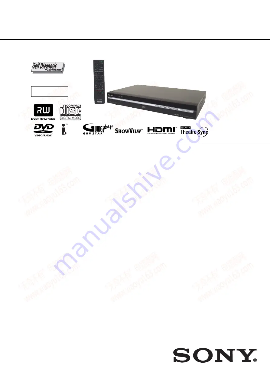
Photo: RDR-HX750

RMT-D247P

(GX350/HX650)

(HX750/HX950)

(HX750/HX950)

System

Laser:

 Semiconductor laser

Channel coverage: 

PAL/SECAM (B/G, D/K, I, L)
VHF: E2 to E12, R1 to R12, F2 to F10, 
Italian A to H, Ireland A to J, South 
Africa 4 to 11, 13
UHF: E21 to E69, R21 to R69, B21 to 
B69, F21 to F69
CATV: S01 to S05, S1 to S20, France 
B to Q
HYPER: S21 to S41

The above channel coverage merely ensures 
the channel reception within these ranges. It 
does not guarantee the ability to receive 
signals in all circumstances. For details, see 
“Receivable channels”.

Video reception:

 Frequency synthesizer 

system

Audio reception:

 Split carrier system

Aerial out:

 75-ohm asymmetrical aerial 

socket

Timer:

 Clock: Quartz locked/Timer 

indication: 24-hour cycle (digital)/
Power back-up duration: 1 hour 

Video recording format:

 MPEG-2, 

MPEG-1

Audio recording format/applicable 

bit rate:

 Dolby Digital 2 ch 

256 kbps/128 kbps (in EP, SLP, and 
SEP mode), PCM

Inputs and outputs

LINE 2 OUT
(AUDIO):

 Phono jack/2 Vrms/10 kilohms

(VIDEO):

 Phono jack/1.0 Vp-p

(S VIDEO):

 4-pin mini DIN/Y: 1.0 Vp-p, 

C: 0.3 Vp-p (PAL)

LINE 2 IN
(AUDIO):

 Phono jack/2 Vrms/more than 

22 kilohms

(VIDEO):

 Phono jack/1.0 Vp-p

(S VIDEO):

 4-pin mini DIN/Y: 1.0 Vp-p, 

C: 0.3 Vp-p (PAL)

LINE 3 – TV:

 21-pin 

CVBS OUT 
S-Video/RGB OUT (upstream)

LINE 1/DECODER:

 21-pin 

CVBS IN/OUT 
S-Video/RGB IN 
Decoder

DV IN:

 4-pin/i.LINK S100

DIGITAL OUT (COAXIAL):

 Phono jack/

0.5 Vp-p/75 ohms

COMPONENT VIDEO OUT 

(Y, P

B

/C

B

, P

R

/C

R

):


Phono jack/Y: 1.0 Vp-p, 
P

B

/C

B

: 0.7 Vp-p, P

R

/C

R

: 0.7 Vp-p

G-LINK:

 mini jack

HDMI OUT:

 HDMI 19-pin-Standard 

Connector

USB:

USB jack Type A (For connecting 
digital still camera, Memory card 
reader and USB memory)
USB jack Type B (For connecting 
PictBridge-compatible printers)

General

Power requirements:

 220-240 V AC, 

50/60 Hz

Power consumption:


Dimensions (approx.):


4

RDR-GX350: 22 W
RDR-HX650: 40 W
RDR-HX750/HX950: 44 W

30 

×

 66.5 

×

 286 mm (width/height/

depth) incl. projecting parts

Hard disk drive capacity:


RDR-HX650/HX750: 160 GB
RDR-HX9

RDR-HX750: AEP, UK/HX950: AEP, UK:

RDR-HX750/HX950:

RDR-HX750/HX950:

50: 250 GB

Mass (approx.): 

RDR-GX350 : 3.6 kg
RDR-HX650/HX750/HX950: 4.4 kg

RDR-HX750/HX950: 

Operating temperature:

 5

°

C to 35

°

C

Operating humidity:

 25% to 80%

Supplied accessories:


Mains lead (1)
Aerial cable (1)
Remote commander (remote) (1)

Set top box controller (1)
R6 (size AA) batteries (2)

Specifications and design are subject to 
change without notice.

Ver. 1.2  2007.10

Revised-2

www. xiaoyu163. com

QQ 376315150

9

9

2

8

9

4

2

9

8

TEL 13942296513

9

9

2

8

9

4

2

9

8

0

5

1

5

1

3

6

7

3

Q

Q

TEL  13942296513  QQ  376315150  892498299 

TEL  13942296513  QQ  376315150  892498299 

http://www.xiaoyu163.com

http://www.xiaoyu163.com

Summary of Contents for RDR-GX350

Page 1: ...an 22 kilohms VIDEO Phono jack 1 0 Vp p S VIDEO 4 pin mini DIN Y 1 0 Vp p C 0 3 Vp p PAL LINE 3 TV 21 pin CVBS OUT S Video RGB OUT upstream LINE 1 DECODER 21 pin CVBS IN OUT S Video RGB IN Decoder DV IN 4 pin i LINK S100 DIGITAL OUT COAXIAL Phono jack 0 5 Vp p 75 ohms COMPONENT VIDEO OUT Y PB CB PR CR Phono jack Y 1 0 Vp p PB CB 0 7 Vp p PR CR 0 7 Vp p G LINK mini jack HDMI OUT HDMI 19 pin Standar...

Page 2: ...G DO NOT APPROACHTHE LASER EXITWITH THE EYE TOO CLOSELY IN CASE IT IS NECESSARY TO CONFIRM LASER BEAM EMISSION BE SURE TO OBSERVE FROM A DISTANCE OF MORETHAN 25 cm FROMTHE SURFACE OF THE OBJECTIVE LENS ON THE OPTICAL PICK UP BLOCK CAUTION The use of optical instrument with this product will increase eye hazard Unleaded solder Boards requiring use of unleaded solder are printed with the lead free m...

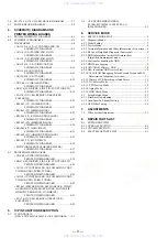
Page 3: ...Track etc 1 16 Erasing and Editing 1 17 Before Editing 1 17 Erasing and Editing a Title 1 17 Erasing and Editing a Chapter 1 18 Creating and Editing a Playlist 1 18 Dubbing HDD y DVD 1 19 Before Dubbing 1 19 HDD DVD Dubbing 1 19 Dubbing Using Dubbing List 1 19 Making a Backup Disc DVD Backup 1 20 DV Camcorder Dubbing 1 20 Before DV Camcorder Dubbing 1 20 Dubbing an Entire DV Format Tape DV One Tou...

Page 4: ...OARD 4 47 RD 065 POWER BLOCK EMMA BLOCK VIDEO AUDIO BLOCK MEMORY BLOCK SATA IDE IF HDMI DV USB BLOCK DVD DRIVE PRINTED WIRING BOARD 4 51 FL 178 DV USB REMOCON RECEIVER POWER SW PRINTED WIRING BOARD 4 55 5 IC PIN FUNCTION DESCRIPTION 5 1 IT CONTROL IC IC101 LC87F06J2A F58W3 E AV 114 BOARD 5 1 5 2 AV ENCODER DECODER IC IC1001 MC10050F1 105 505 LU1 A RD 65 BOARD 5 3 6 SERVICE MODE 6 1 SERVICE MODE MA...

Page 5: ...D drive unit while the tray remains under the state as described above the situation cannot be improved 2 If the tray cannot be ejected while the disc is not inserted Execute the forced ejection Insert a DVD ROM DVD test disc DVD software available on the market or the like on the tray and try to close the tray There are cases that it recovers the trouble 3 Contents of forcedly ejected blank disc ...

Page 6: ... the 4 digit Input No on the screen using the service remote controller 7 The model name setting method is complete Screen disappears Upon completion of the model name setting be sure to press both ENTER and 3 simultaneously on the service remote controller without fail It sets the remote control code 3 Fig 1 S company P company selection Table1 Correspondence table between tentative model name an...

Page 7: ...n conditions Failure to physically identify the HDD no connection defective HDD interface error Physical identification of HDD possible but not identified Physical identification of HDD possible HDD identified but failure in logical formatting Physical identification of HDD possible HDD identified and correct logical formatting HDD correctly identified Details on HDD data are described below Blank...

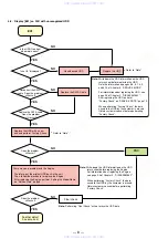
Page 8: ...he original HDD back in the unit Then follow the procedure to replace the Engine After replacing the Engine perform Setting the Model Name on Service Note page 6 YES Does the problem still occur Another defect has occurred YES Unauthorized HDD Replace the SATA Cable NO NO NO NO NO Final check NO Replace the HDD Note Performing Final Check will not erase the HDD data Refer to Note Refer to Note Not...

Page 9: ... playing a VIDEO MP3 or JPG the contents freeze Any error is not displayed on the FLD Display the ATA ATAPI history by using HDD Access Flow on page 6 10 Is the HDD free from abnormal noises YES Does the history show no errors YES NO NO END Final check Replace the HDD Has the Final check ended with success YES NO Note Performing Final Check will not erase the HDD data Refer to Note www xiaoyu163 c...

Page 10: ...YS INIT 07 03 19 12 36 06 HDD Zero MR 07 03 19 12 36 06 HDD Initialze 07 03 19 12 36 06 HDD Zero MR 07 03 19 12 27 27 Status NG 4 6 Factory Check 1 Pull out and then reconnect the AC cable 2 Press ESC key followed by P RUN key to start Formatting 3 When B COMPLETE appears the Factory Check is complete 4 Press Power button The unit starts normally When Factory Check has finished completely without ...

Page 11: ...omplete 6 Power OFF Test 6 0 0 0 0 0 0 0 7 0 0 0 0 0 0 0 8 0 0 0 0 0 0 0 9 0 0 0 0 0 0 0 A 0 0 0 0 0 0 0 B COMPLETE 1 0 0 0 0 0 0 0 8 1 0 0 0 0 0 0 HDD ERR 01 HDD ERR 02 aError display HDD ERR 81 HDD ERR 82 HDD ERR 03 HDD ERR 04 HDD ERR 05 HDD ERR 07 HDD ERR 09 2 0 0 0 0 0 0 0 3 H M S 8 0 0 0 0 0 0 0 aNormal display 8 3 0 0 0 0 0 0 H M S 8 4 COMPLETE 8 2 H M S 4 H M S 5 F M H M S 80 Performance Ch...

Page 12: ...d AV 118 AG EM AV 118 BG EM Board VDC Board VDC 001 AG Board Flexible Flat Cable FVR 001 FFC FVA 002 FFC PV 145 HARNESS PAE 002 HARNESS not supplied Type AS BS CS DS Destination AEP1 AEP2 UK Russian AEP1 AEP2 AEP3 AEP1 UK Russian AEP2 AEP1 AEP2 Model RDR GX350 RDR HX650 RDR HX750 RDR HX950 RD 065 AS RD 065 CS RD 065 BS RD 065 DS RD 065 BS RD 065 DS RD 065 BS RD 065 DS RD 065 BS RD 065 DS RD 065 BS...

Page 13: ...disconnect the recorder from the wall outlet To disconnect the AC power cord mains lead grasp the plug itself never pull the cord On placement Place the recorder in a location with adequate ventilation to prevent heat build up in the recorder Do not place the recorder on a soft surface such as a rug that might block the ventilation holes Do not place the recorder in a confined space such as a book...

Page 14: ...rd playback on this product is not guaranteed b Notes Some DVD RWs DVD Rs DVD RWs DVD Rs DVD RAMs or CD RWs CD Rs cannot be played on this recorder due to the recording quality or physical condition of the disc or the characteristics of the recording device and authoring software The disc will not play if it has not been correctly finalised For more information see the operating instructions for t...

Page 15: ...ent Video Out to Progressive in the Video In Out setup to send progressive video signals For details see Component Video Out on page 115 E HDMI input jack Use a certified HDMI cord not supplied to enjoy high quality digital picture and sound through the HDMI OUT jack When connecting a Sony TV that is compatible with the HDMI control function see page 18 To see the signals from the connected set to...

Page 16: ... Notes Do not connect your TV s audio output jacks to the LINE IN R AUDIO L jacks at the same time This will cause unwanted noise to come from your TV s speakers With connection B do not connect the LINE IN R AUDIO L and LINE 2 OUT R AUDIO L jacks to your TV s audio output jacks at the same time This will cause unwanted noise to come from your TV s speakers With connection A after you have complet...

Page 17: ...IDE TV 1 continued 24 Progressive When you connect a progressive format TV to this recorder using the COMPONENT VIDEO OUT jacks select Compatible HDD caution messages Read the HDD caution messages and press ENTER 4 Select Finish Setup using M m and press ENTER Easy Setup is completed To return to the previous step Press O RETURN z Hint If you want to run Easy Setup again select Easy Setup in the B...

Page 18: ...ipment s output jack connected to the input jack of this recorder This may cause noise feedback Do not connect more than one type of video cord between the recorder and your TV at the same time Connecting to the LINE 2 IN jacks on the front panel OUTPUT S VIDEO AUDIO L R VIDEO VCR etc Audio video cord not supplied S video cord not supplied DVD recorder Signal flow to LINE 2 IN 28 Connecting an Ext...

Page 19: ...s for recorder to stop recording To watch another TV programme while recording If your TV is connected to the T LINE 3 TV jack set your TV to the TV input using the TV DVD button and select the programme you want to watch If your TV is connected to the LINE 2 OUT or COMPONENT VIDEO OUT jacks set the TV to TV input using the TV t button page 21 TV Direct Rec for SMARTLINK connections only When the ...

Page 20: ...may take a few seconds for the thumbnail pictures to be displayed After editing the title thumbnail picture may change to the first scene of the recording title After dubbing the title thumbnail picture set on the source recording is cancelled 4 Displaying the Playing Time and Play Information You can check the playing time of the current title chapter track or disc Also you can check the disc nam...

Page 21: ...me is short You can edit or record on the disc even after finalising Finalising is necessary when playing on any equipment other than this recorder After finalising you cannot edit or record on the disc If you want to record on it again unfinalise page 41 or reformat the disc page 42 However if you reformat the disc all recorded contents will be erased Finalising is necessary The disc can be playe...

Page 22: ...ently selected time slot Use to select a different time slot z Hint You can also move the cursor to the Menu Bar by pressing MENU If you are having trouble displaying the television programme list please check the following Your country region must be set correctly page 23 The clock must be set correctly If the clock is not set set it manually page 109 This recorder downloads the GUIDE Plus data s...

Page 23: ...keywords press the yellow button Add You can register up to 16 keywords To cancel the registration select a keyword and press the red button Delete 3 Press ENTER To change the profile settings Repeat from step 1 above 1 Select My TV in the Menu Bar and press ENTER The programmes that match the profile conditions are displayed 2 Select a programme using M m and press ENTER To set a programme for ti...

Page 24: ...just sound Programmes are recorded in the following aspect ratio In the original aspect ratio when recording to the HDD when HDD Recording Format is set to Video Mode Off in the Recording setup page 122 DVD RWs DVD Rs VR mode In 4 3 when recording to DVD RWs DVD Rs When recording to DVD R DLs Video mode the title is divided when the layer switches The recorder automatically receives and records st...

Page 25: ...recording press x REC STOP b Note If you turn off the recorder during recording recording is stopped Using the Quick Timer function normal recording continued 56 You can adjust the picture quality from the connected equipment such as a TV or VCR by selecting a preset setting You can also adjust the picture quality by changing detailed settings and store up to three settings in the memory 1 Press S...

Page 26: ...or if you select PCM as recording mode You cannot select L1 in step 2 if LINE 1 In is set to Decoder in the Video In Out setup page 115 RW RWVR RWVideo RVR R HDD RVideo INPUT REC MODE z REC x REC STOP DVD HDD programme position 60 Playback Playing the Recorded Programme DVD DivX video file only 1 Press HDD or DVD If you select DVD insert a disc see 1 Inserting a Disc on page 31 If you insert a DVD...

Page 27: ...ts within the same title You can play repeatedly all the titles tracks files or a single title chapter track on the HDD or a disc 1 Press PLAY MODE during playback The Play Mode menu appears 2 Select Repeat and press ENTER 3 Select an item to be repeated using M m Repeat Title for HDD DVDs DATA DVDs 1 DATA CDs 1 repeats the current title Repeat Chapter for HDD DVDs repeats the current chapter Repe...

Page 28: ...tarts only recording in the following cases when the programme positions are preset differently between the recorder and the connected TV when watching the programme from the external equipment connected to your TV The picture tuned by the recorder pauses when TV Pause is set to Recorder s Tuner in the Options 2 setup page 128 You may not be able to use the TV Pause function depending on some TVs ...

Page 29: ...r the editing points may be slightly different from the point you selected when you dub the titles by High speed dubbing Erasing and Editing a Title This section explains the basic edit functions Note that editing is irreversible To edit DVD RWs DVD Rs VR mode without changing the original recordings create a Playlist title page 76 1 Press TITLE LIST For DVD RWs DVD Rs in VR mode switch the Title ...

Page 30: ... X To return to the beginning of the chapter press X and then press 4 Press ENTER The chapter is divided into two RWVR HDD RVR M m ENTER TITLE LIST M m X Dividing a chapter Divide continued 76 1 After step 4 of Erasing and Editing a Chapter select Erase Move 2 Select a chapter using and press ENTER 3 Select Erase and press ENTER The display asks for confirmation 4 Select Yes and press ENTER The ch...

Page 31: ...DUB button in the following cases Dub the title using Dubbing List page 80 When dubbing the title recorded in MN6 mode or longer duration mode to a DVD RW DVD R When dubbing the title recorded in HQ mode to a DVD Copy protection signals Dubbing Copy Free No copy protection signal Copy Once HDD RWVR RWVideo RW RVR R RVideo HDD RWVR RVR RW RWVR RWVideo R HDD RVR RVideo 80 Dubbing Using Dubbing List ...

Page 32: ...out i LINK on page 140 How chapters are created The contents dubbed to the HDD or DVD become a single title This title is divided into chapters When dubbing to the HDD or a DVD RW DVD R VR mode and when Auto Chapter HDD VR is set to On in the Recording setup page 121 each shooting session on the tape becomes a chapter on the disc For other discs the recorder divides the title into chapters accordi...

Page 33: ...ou can play audio tracks using the Title List Press TITLE LIST Then select a track and press ENTER b Note When any video titles are recorded on a DATA DVD the MP3 audio tracks on that DATA DVD cannot be played To lock the recorder Child Lock You can lock all of the buttons on the recorder so that the settings are not cancelled by mistake When the recorder is turned off hold down x on the recorder ...

Page 34: ...s Assign albums a genre Change the track order Notes on copying You cannot copy audio tracks on the HDD to discs or USB devices Some audio tracks may not be copied depending on the file size You cannot copy audio tracks if the HDD is full or almost full An album name and MP3 audio track name are also copied However there may be some names that cannot be copied When copying is stopped partway track...

Page 35: ...speed changes as follows fast reverse fast forward m T t M m T T t t M When you press and hold the button fast forward fast reverse continues at the selected speed untilyou release the button To resume normal playback press H X pause Pauses playback To resume normal playback press H Playing repeatedly Repeat continued 96 You can play the contents of the HDD or connected USB device in the order you...

Page 36: ...ect Copy and press ENTER 12Select the destination album using M m and press ENTER To cancel select No b Note Albums or JPEG image files are not copied to the HDD in the following cases when the HDD disc space is insufficient for copying when there are already the maximum number of files and or albums on the HDD You can copy the edited JPEG image albums to a DVD RW DVD R Video mode A slideshow is a...

Page 37: ...appears Switch to the album list if necessary 2 Select a JPEG image file using M m and press ENTER The selected JPEG image file is displayed on the entire screen To display the detailed information 1 Select a JPEG image file and press 2 Select Detailed Information and press ENTER The detailed information for the selected JPEG image file appears 1 Follow steps 1 to 4 of Using the Photo Album List T...

Page 38: ... The Disc Setup setup appears with the following options The default settings are underlined Basic Input Disc Name You can label a disc For details see page 38 Protect Disc You can protect a disc against erasure For details see page 39 Format DVD RW DVD RW only The recorder automatically starts formatting in VR mode or Video mode whichever is selected below when a new unformatted DVD RW is inserte...

Page 39: ...nued 112 Skip CH System Select the region to get the best broadcast reception AFT If the Auto Fine Tuning function does not work effectively select Off and press m Press to obtain a clearer picture and press ENTER Sound System Select an available TV system page 112 Name Changes or enters a new station name up to 5 characters The recorder must receive programme position information e g SMARTLINK in...

Page 40: ... Level If the playback sound is distorted set this item to Compression The recorder reduces the audio output level This function affects the output of the following jacks LINE 2 OUT R AUDIO L jacks LINE 3 TV jack LINE 1 DECODER jack External Audio b Note When receiving audio input signals from the DV input jack the recorder automatically selects Stereo or Bilingual regardless of the External Audio...

Page 41: ...20 73 115 MN19 79 120 MN18 LSP 84 130 MN17 90 140 MN16 96 150 MN15 ESP 100 155 MN14 105 165 MN13 110 175 MN12 115 185 MN11 120 190 MN10 125 200 MN9 LP 135 210 MN8 150 235 MN7 165 265 MN6 EP 200 315 MN5 235 370 MN4 SLP 270 425 MN3 SEP 340 530 MN2 405 635 MN1 455 710 Recording mode Approx recording time hours DVD RW DVD RW DVD R DVD R DVD R DL DVD R DL PCM 2 1 hr 1 min 1 hr 51 min MN32 HQ 1 hr 1 min...

Page 42: ...l Control Change Level display appears 8 Enter your four digit password using the number buttons and press ENTER 9 Select the level The lower the value the stricter the limitation Discs rated higher than the selected level will be restricted 10 Press ENTER The Parental Control setting is complete To cancel the Parental Control setting for the disc select Off in step 9 Change Password 1 Select Pare...

Page 43: ...rts the connected USB device if it does not respond to the recorder If the connected USB device still does not work properly try following Turn the connected USB device off and on again Disconnect and then connect the USB cable Confirm Printer Displays the manufacturer and model name of the printer connected to the recorder Note that this function may not work depending on the printer TV Pause Sel...

Page 44: ...he HDMI cord again The HDMI OUT jack is connected to a DVI device DVI jacks do not accept audio signals The equipment connected to the HDMI OUT jack does not conform to the audio signal format In this case set Audio Output to PCM in the HDMI Output setup page 126 GUIDE Plus system Sound continued 132 Sound distortion occurs Set Tuner Level in the Audio In setup to Compression page 116 Sound is noi...

Page 45: ...ttons do not function and LOCKED appears in the front panel display The recorder is locked Cancel the Child Lock page 61 88 The disc tray does not open and TRAYLOCKED appears in the front panel display Contact your Sony dealer or local authorized Sony service facility REPAIR appears in the front panel display The recorder s repair function is activated to repair the hard disk drive or disc when th...

Page 46: ...der an album can be played For JPEG image files the recorder can load up to 99 albums and or up to 999 files under an album on a DATA CD DATA DVD or the connected USB device at a time To view unloaded albums reload them Proceeding to the next or another album may take some time The image size that can be displayed is limited The following image sizes can be displayed width 160 5 120 pixels by heig...

Page 47: ...y button 60 88 104 The N button has a tactile dot G x stop button 60 88 94 104 H z REC button 31 I x REC STOP button 31 J HDD button indicator 31 DVD button indicator 31 K PROGRAM buttons 31 The button has a tactile dot L INPUT input select button 59 M LINE 2 IN S VIDEO VIDEO L MONO AUDIO R jacks 27 N ONE TOUCH DUB button 86 O DV IN jack 84 P USB jack type A 92 98 Q PictBridge USB jack type B 106 ...

Page 48: ...a Chile cl China cn Denmark dk Finland fi France fr Germany de Hong Kong hk India in Indonesia id Italy it Japan jp Korea kr 1325 1324 1412 1426 1415 1611 1608 1620 1821 1907 0519 1905 0308 2023 2008 0702 2119 Malaysia my Mexico mx Netherlands nl New Zealand nz Norway no Pakistan pk Philippines ph Portugal pt Russia ru Singapore sg Spain es Sweden se Switzerland ch Taiwan tw Thailand th United Kin...

Page 49: ...sembly Page 2 2 Hard disk Page 2 5 Front panel section Page 2 3 FR 274 board FL 178 board Page 2 3 DVD drive Page 2 4 Power supply block Page 2 6 AV 114 118 board Page 2 5 VDC 001 board Page 2 6 Type AS BS only DC fan Page 2 4 www xiaoyu163 com QQ376315150 9 9 2 8 9 4 2 9 8 TEL 13942296513 9 9 2 8 9 4 2 9 8 0 5 1 5 1 3 6 7 3 Q Q TEL 13942296513 QQ 376315150 892498299 TEL 13942296513 QQ 376315150 8...

Page 50: ...ee screws special front point screw 4 Upper case 1 The stiff wire 3 Two claws 4 Tray cover assembly 2 Open the tray Hole www xiaoyu163 com QQ376315150 9 9 2 8 9 4 2 9 8 TEL 13942296513 9 9 2 8 9 4 2 9 8 0 5 1 5 1 3 6 7 3 Q Q TEL 13942296513 QQ 376315150 892498299 TEL 13942296513 QQ 376315150 892498299 http www xiaoyu163 com http www xiaoyu163 com ...

Page 51: ... CN202 9 Flexible flat cable 17core CN203 1 Flexible flat cable FLR 010 5core q FR 274 board 4 Connector 6p CN101 3 Connector 10p CN102 except GX350 2 4 FR 274 BOARD FL 178 BOARD www xiaoyu163 com QQ376315150 9 9 2 8 9 4 2 9 8 TEL 13942296513 9 9 2 8 9 4 2 9 8 0 5 1 5 1 3 6 7 3 Q Q TEL 13942296513 QQ 376315150 892498299 TEL 13942296513 QQ 376315150 892498299 http www xiaoyu163 com http www xiaoyu1...

Page 52: ...S BS only 4 Connector 4p CN203 wf Connector 13p CN4501 ws Two screws PSW3 6 wd Clamp L35 wg DVD drive 5 Connector 13p CN201 qg Two screws BV3 qh Four screws BV3 qf Remove the harness 6 Harness 7p CN5604 ql 1 The wire pin that holds the harness is set up 1 Two screws BV3 2 DC fan Air flow www xiaoyu163 com QQ376315150 9 9 2 8 9 4 2 9 8 TEL 13942296513 9 9 2 8 9 4 2 9 8 0 5 1 5 1 3 6 7 3 Q Q TEL 139...

Page 53: ... 1 Flexible flat cable 11core CN106 2 Flexible flat cable 17core CN105 9 AV 114 118 board 6 Connector 5core CN301 Type CS DS only 5 Earth plate 7 Two screws BV3 8 Two screws BV3 4 Flexible flat cable FRA 006 40core CN101 www xiaoyu163 com QQ376315150 9 9 2 8 9 4 2 9 8 TEL 13942296513 9 9 2 8 9 4 2 9 8 0 5 1 5 1 3 6 7 3 Q Q TEL 13942296513 QQ 376315150 892498299 TEL 13942296513 QQ 376315150 8924982...

Page 54: ...or 12p CN202 1 Flexible flat cable 24core CN106 1 Connector 12p CN202 3 Two board holders 2 Three screws BV3 4 Spacer 5 Power supply block www xiaoyu163 com QQ376315150 9 9 2 8 9 4 2 9 8 TEL 13942296513 9 9 2 8 9 4 2 9 8 0 5 1 5 1 3 6 7 3 Q Q TEL 13942296513 QQ 376315150 892498299 TEL 13942296513 QQ 376315150 892498299 http www xiaoyu163 com http www xiaoyu163 com ...

Page 55: ...ION NOTE When replacing parts refer to SERVICE NOTE 5 CHANGED POINTS OF SERVICE MANUAL Revised 2 See page 12 www xiaoyu163 com QQ376315150 9 9 2 8 9 4 2 9 8 TEL 13942296513 9 9 2 8 9 4 2 9 8 0 5 1 5 1 3 6 7 3 Q Q TEL 13942296513 QQ 376315150 892498299 TEL 13942296513 QQ 376315150 892498299 http www xiaoyu163 com http www xiaoyu163 com ...
Page 56: ...yu163 com QQ376315150 9 9 2 8 9 4 2 9 8 TEL 13942296513 9 9 2 8 9 4 2 9 8 0 5 1 5 1 3 6 7 3 Q Q TEL 13942296513 QQ 376315150 892498299 TEL 13942296513 QQ 376315150 892498299 http www xiaoyu163 com http www xiaoyu163 com ...

Page 57: ... CONVERTER F1 F2 SEG1 16 GRD1 12 FLDATA FLCLK FLSTB V 12V VEE ND201 FLUORESCENT DISPLAY S201 203 204 S207 213 FUNCTION SWITCH D212 214 HDD DVD IC101 REMOTE CONTORL RECEIVE IR V 5USB S VIDEO VIDEO AUDIO R AUDIO L MONO LINE2 IN CN104 CN105 USB BTYPE USB ATYPE DV IN CN103 KEY1 2 S101 POWER S102 ONE TOUCH DUB SDA SCL IC1201 IC1221 512Mbit x2 DDR SDRAM 17 DADRS0 12 DDATA0 31 IC201 64Mbit SDRAM MD0 15 M...

Page 58: ... DSCL CEC AMUTE1 X525P RFTHRU FANCTL TUON SWVION9V P_CONT SWVION5V TU_DCCON 57 65 29 99 6 98 100 79 37 73 FLON FLDATA FLCLK FLSTB LED_HDD2 LED_A_TV LED_D_TV LED_DIVX LED_PLTV KEY1 KEY2 KEY3 IR 63 49 51 50 97 96 95 94 93 17 18 19 7 52 54 60 61 62 64 74 IC101 1 5 IT CONTROLLER TX1 TX2 SDA SCL CEC0 DDC_SW2 27 28 69 38 SDET2 XAMUTE2 RCSEL1 RCSEL2 P_SAVE CSYNCIN BLANK FUNC_ON SQUEEZE FUNC AVLOUT AVLTH ...

Page 59: ...12Mbit X 2 DDR SDRAM DDATA0 7 16 23 DDATA8 15 24 31 IC1201 IC1221 DBA0 DBA1 DCLKO DCLKNO DWE DCAS DRAS DCS0B DCKE DDM0 DDM2 DDQS0 DDQS2 DDM1 DDM3 DDQS1 DDQS3 29 32 35 40 28 41 42 DQ0 DQ15 A0 A12 2 4 5 7 8 10 11 13 54 56 57 59 60 62 63 65 BA0 BA1 CK CK WE CAS RAS CS CKE LDM HDM LDQS UDQS B4 A4 C5 B5 E1 E2 D1 D2 D3 E4 C4 D4 E5 26 27 45 46 21 22 23 24 44 20 47 16 51 B3 A3 C1 B1 C2 B2 A2 C3 D5 F3 J1 F...

Page 60: ...3 6 S201 213 212 OPEN CLOSE HDD DVD S203 204 207 REC STOP INPUT SELECT REC S208 211 CH CH PLAY STOP TO FROM AV 114 118 BOARD CN105 SEE PAGE 3 4 SDRDQ0 15 7 SDRA0 SDRA10 SDRA0 10 SDRDQ0 SDRDQ15 51 49 46 42 40 36 34 30 31 35 37 41 43 47 50 52 SDRABP SDRWE SDRCAS SDRRAS SDRCS SDRCLK SDRCKE IC105 SDRAM 21 24 27 32 19 DQ0 DQ15 A0 A9 2 3 5 6 8 9 11 12 39 40 42 43 45 46 48 49 A10 AP XWE XCAS XRAS XCS CLK...

Page 61: ...RD FL 178 BOARD FR 274 BOARD IC5802 IC201 64Mbit SDRAM IC5602 SATA BRIDGE V 12VA V 5A IN IC5103 DV PHY 18 5 JA5801 L4551 V 3DS V 3V_D L5601 V 3D EMI 1 3 2 _ IC1302 VREF_D VREF_D 8 1 3 2 _ IC200 EEPROM IC1102 64Mbit FLASH ROM IC3201 AUDIO DAC IC3202 AUDIO LPF IC3101 AUDIO ADC IC4701 4703 BUFFER V 3D V 3D IC3701 BUFFER IC3702 AND GATE IC5801 IC5701 SPDIF SELECT IC5203 AND GATE V 3D 10 14 1 CN5201 6 ...

Page 62: ...950 w w w x i a o y u 1 6 3 c o m Q Q 3 7 6 3 1 5 1 5 0 9 9 2 8 9 4 2 9 8 T E L 1 3 9 4 2 2 9 6 5 1 3 9 9 2 8 9 4 2 9 8 0 5 1 5 1 3 6 7 3 Q Q TEL 13942296513 QQ 376315150 892498299 TEL 13942296513 QQ 376315150 892498299 http www xiaoyu163 com http www xiaoyu163 com ...
Page 63: ...D 2R GND 2L 2V 2C 2V GND GND GND YP_OUT HPD X525P DDC_SW 1 XRST1 GND DSCL GND GND R_IN CEC GNDA GND DSDA B_IN GND HST_TO_M GND ASCK GND DAT_TO_M GND HSM_TO_T MRST GND L_IN AMUTE1 L_OUT G_I N C R_I N Y_I N C_OUT DAM_TO_T Y_OUT P_CONT2 GND R_OUT GND CB_OUT CR_OUT DITV FLPO N V 12RIE FLDATA PLT V KEY3 KEY2 GND FLCLK A_TV KEY1 FLST B D_TV HDD2 IR GND V 5F GND 2Y 2C 2R 2L GN D GN D 2V GN D SDET 2 GND I...

Page 64: ...stic curve B unless otherwise noted 2 non flammable resistor 5 fusible resistor C panel designation f internal component C adjustment for repair G IN OUT direction of B line U B Line V B Line Circled numbers refer to waveforms Voltages are dc between measurement point and ground Readings are taken with a color bar signals on DVD reference disc Readings are taken with a digital multimeter DC 10MΩ V...

Page 65: ...755 JA751 150 R754 JL712 220k R701 4 7k R753 0uH L751 R703 0 100p C752 JL713 1k R751 0 1 C751 JL714 4 7k R752 100p C753 R226 15k 0 R161 JL153 0 1 C134 0 R201 GND L2_LIN C2IN KEY1 KEY2 KEY3 DBGP 2 DBGP 1 DBGP 0 LED_PLTV LED_DIVX LED_D_TV LED_A_TV LED_HDD2 DAT_TO_ M DAM_TO_ T ASCK HSM_TO_ T DDC_SW 1 DDC_SW 2 AVLTH SQU FUNC_ON RCSEL2 RCSEL1 XAMUTE2 FUNC_IN AGC P_CONT2 AMUTE1 TXD1 TU_DCCON HOTPLUG AVL...

Page 66: ...8E 50V 100p C322 50V 1 F C323 50V 0 1 F C328 UDZSTE 179 1B D302 Q304 2SD2153T100V Q309 2SC5876T106QR 1SS355TE 17 D304 16V 100 C312 25V 22 C205 16V 0 1 B C208 SWVION9 V 0 5A IC317 32V 0 R251 1 2 3 4 5 6 7 8 9 10 11 12 13 14 15 16 17 18 19 20 21 22 23 24 24P CN302 Y_IN BTOMAIN GTOMAIN C R_I N GND V 5V I V 5V I GND GND V 32V P_CONT2 DET_ANT ANT5V_SW DT_TUON FAN EV 5 8V EV 5 8V GND EV 12 1V P_CONT GND...

Page 67: ...10 10k R312 1SS355TE 17 D303 22k R314 XP4401 Q311 25V 0 1 F C324 180k R313 0 5 100k R315 0 5 22k R316 V 32V 0uH L305 50V 10 C326 JL302 JL303 JL304 JL310 JL318 JL328 JL327 JL321 JL324 V 5R8E 50V 100p C322 50V 1 F C323 50V 0 1 F C328 UDZSTE 179 1B D302 Q304 2SD2153T100V Q309 2SC5876T106QR 1SS355TE 17 D304 16V 100 C312 25V 22 C205 16V 0 1 B C208 SWVION9 V 0 5A IC317 32V 0 R251 1 2 3 4 5 5 P CN301 GND...

Page 68: ...9 UMZ6 8N T106 D410 UMZ6 8N T106 D413 UMZ6 8N T106 D415 UMZ6 8N T106 D416 UMZ6 8N T106 D414 UMZ6 8N T106 NNCD3 9F T1B D421 NNCD3 9F T1B D422 47 R455 R421 1 8M R420 1 8M L801 0uH L802 0uH 0 R801 C478 0 C485 0 25V 0 1 F C463 UMZ6 8N T106 D801 Y_I N TU_LIN TU_RIN TU_VIN RTOMAIN AV1_LOUT AV2_LOUT AV1_ROUT AV2_ROUT RGBOUT R COUT GOUT BOUT BIN GIN R CIN AV1_V YOUT AV2_V YIN AV2_V YOUT AV1_V YIN P_SAVE 2...

Page 69: ...50V 4 7 C541 50V 4 7 C542 3 9k R534 3 9k R535 HN1C03FU TE85R Q506 AV2_V YIN AV2_V YOUT AV1_ROUT AV1_LOUT 50V 4 7 C544 470 R550 100k R555 100k R554 HN1C03FU TE85R Q507 3 9k R557 100 R553 3 9k R556 AV2_ROUT 100 R551 50V 4 7 C543 470 R552 AV2_LOUT DTA124EUA T106 Q508 1SS355TE 17 D528 16V 100 C545 V 12R1 SAMUTE 680 R561 15k R560 10k R558 22k R566 12k R568 25V 22 C547 BTOMAIN 15k R564 680 R565 GTOMAIN ...

Page 70: ...B C631 50V 560p C630 50V 560p C633 1k R623 1k R626 TU_RIN TU_LIN 25V 0 1 F C627 25V 0 1 F C626 JL656 JL657 JL65 8 JL659 JL660 V 5BB 50V 2200p B C602 50V 2200p B C603 JL604 0uH L604 0uH L605 10V 100 C609 50V 100p C604 JL603 JL605 JL608 JL609 JL610 JL611 JL612 JL616 JL617 V 32V V 5TU 0 R603 35V 47 C611 ISA1602AM1TP 1EF Q602 ISA1602AM1TP 1EF Q601 10k R605 AGC JL618 L601 0uH JL60 1 JL602 10k R606 AFT ...

Page 71: ... 21 22 23 24 24P CN106 EM I G O I F10 3 EM I G O I F10 2 EM I G O I F106 EM I G O I F10 4 EMI G O I F105 EMI G O I F107 EM I G O I F10 1 100 R176 1 3 5 7 0 R182 0 R183 0 R184 16V 0 01 B C242 0 R185 4 7 k R186 4 7 k R187 50V 1000p B C235 50V 1000p B C236 50V 1000p B C246 50V 1000p B C233 50V 1000p B C240 50V 1000p B C239 50V 1000p B C243 50V 1000p B C250 50V 1000p B C251 50V 1000p B C247 16V 0 1 F ...

Page 72: ...4 JL242 JL245 JL265 JL270 JL274 JL276 JL280 JL285 47 R250 47 R251 47 R252 L201 100uH C207 200V 2700p 1 7 8 9 10 11 12 5 6 14 19 18 17 13 16 20 15 23 24 27 21 28 26 25 22 31 33 35 30 32 36 34 29 42 44 43 40 37 39 38 41 46 52 48 47 45 2 4 49 51 S212 S207 S211 S210 Q206 DTC143TUA T106 D212 SDPB31H3C0100 R231 2 2K GRD1 1 SEG1 2 SEG1 4 SEG1 1 SEG1 0 SEG8 SEG7 SEG5 SEG4 SEG3 GRD1 0 GRD1 GRD9 GRD8 GRD7 G...

Page 73: ...P KEY2 KEY1 IR V 5F GND DV IN USB A type B type USB TPB TPB TPA TPA V 5 D GND D D D GND VFB ONE_TOUCH_DUB USBDM 1 GND GND V 5USB USBDM 2 USBDP 1 USBVFB GND GND USBDP 2 POWER B B CN201 FLR 010 FFC TO FR 274 BOARD IC101 RECEIVER Pict Bridge THROUGH THE RV 001 HARNESS RD 065 TO CN5201 BOARD 6 7 THROUGH THE RV 003 HARNESS RD 065 CN5101 BOARD 6 7 TO RDR HX750 HX950 FL 178 BOARD DV USB REMOCON RECEIVER ...

Page 74: ...3MC L6STFG IC4562 VI N GND CONT NB VOUT 6 3V 1 X6S C4567 6 3V 1 X6S C4570 X6S C4563 1 6 3V 6 3V 1 X6S C4562 S 1112B50MC L7JTFG IC4561 VI N GND CONT NB VOUT TP4565 0 R4575 10uH L4551 50V 1000p B C4553 0 R4559 15k C4526 2 7k R4504 2 7k R4505 2 7k R4507 0 R4573 V 1R 0 V 5D V 1R5_IN V 3D GND D V 3A V 3V V 2R 5 V 5_AO V 1R5_IN V 3D GNDA V 5_VO V 5_VI GND D V 12A V 5_AIN P_CONT2 V 3D V 2R 5 GND D V 1R 8...

Page 75: ...18 RFO AG18 CRC AE17 CTEC AE16 AE18 CBHWBL CID CREG AG11 CBC AE15 CAD AE14 CWAGC AE12 CWHP AE13 CBCO AG12 AG13 EXTR AJ16 AH15 AJ15 AH14 AJ14 ASY AH13 EFM AJ13 RFI_P AH17 RFI_M AH16 AG16 AG17 TEO LE SWRF1 SWRF3 RFP6 FEO LE SWRF2 SWRF4 RFP5 ADIN LE RFP4 AE19 AD18 AD19 AC19 TEST_MODE FPIND TEST1 AD17 DGND A1 DGND F12 DGND F13 DGND F14 DGND F15 DGND F16 DGND K10 DGND K11 DGND L10 DGND N6 DGND N24 DGND...

Page 76: ...FU T5RSOYJF IC3702 6 3V 1 X6S C3707 50V 1000p B C3706 10k R3738 10k R3113 TU_HPD DDC_SW 1 TU_DSDA TU_DSCL TU_CEC HSMTOT X525P AOBCK GI AOD0 AMUTE NSCS SPDIFO C RI RXD PR ROUT AILRCK0 ADCCLKO RXD1 PB BOUT AIBD0 ADPOW SMCKOUT Y GOUT AIBCK0 JTRST SMDOUT YI COUT SPDIFO_LL YOUT BI S MDIN DACCLKO 232RST AOLRCK R3337 R3341 R3302 YP_OUT CR_OUT CB_OUT Y_OUT C_OUT LCHOUT RCHOUT AMUTE1 RCHIN LCHI N XRST1 HST...

Page 77: ...ADD17 RADD18 N21 RADD19 T23 RADD20 R22 RADD21 RADD22 P24 RADD23 GPIO02 RADD24 GPIO03 N19 RADD25 GPIO04 P19 RDATA00 RDATA01 Y21 RDATA02 AA21 RDATA03 U23 RDATA04 V22 RDATA05 T24 RDATA06 U24 RDATA07 N23 RDATA08 R23 RDATA09 RDATA10 T22 RDATA11 T21 RDATA12 P21 RDATA13 N22 RDATA14 N20 RDATA15 R21 FOEB GOEB FWEB GWED AA24 DADD00 B4 DADD01 A4 DADD02 C5 DADD03 B5 DADD04 E1 DADD05 E2 DADD06 D1 DADD07 D2 DAD...

Page 78: ... INTRQ RESERVED DA1 PDIAG DA0 DA2 CS0 CS1 DASP GND GNDD V 3D TP1005 TP1003 TP1004 0 R5693 0 R5692 0 R5690 XRESET 4V 100 C5613 EMI G O I L5601 TP999 16V 0 01 B C5626 16V 0 01 B C562 7 16V 0 01 B C5628 16V 0 01 B C5629 16V 0 01 B C5630 16V 0 01 B C5631 16V 0 01 B C5632 MC10050F1 105 LU1 A IC1001 AT1D00 M4 AT1D01 R1 AT1D02 R4 AT1D03 R2 AT1D04 N5 AT1D05 R3 AT1D06 P4 AT1D07 T1 AT1D08 T2 AT1D09 P5 AT1D1...

Page 79: ...209 50V 1000p B C5219 0 R5201 0 R5202 10 R5222 0 R5216 0 R5217 50V 1000p B C5216 50V 1000p B C5211 16V 0 1 F C5222 50V 1000p B C5223 3 3k R5203 47k R5214 820 R5204 10k R5859 50V 1000p B C5821 50V 1000 p B C5822 V 3HD 1 2 3 4 L5201 0uH 1 2 3 4 L520 2 0uH TP5802 TP5803 TP5804 TP5805 S 2SK2034 TE85L Q5808 0 R5831 0 R5837 UMD2N TR Q5809 3 2 1 6 5 4 10k R5861 4 7k R5862 680 R5863 TP5801 1k R5864 TP5806...

Page 80: ...C516 12k R505 10V 0 1 B C532 10V 0 1 B C504 1k R504 1k R503 1k R507 1k R506 V 12M 1 8 R511 1 8 R510 16V 0 1 F C513 16V 0 1 F C512 1 2 3 4 5 5P CN601 RED BLACK LPS1 GNDD LPS2 50V 1000p B C508 GNDD 1k R603 1k R604 10k R601 10k R602 33k R515 12k R516 50V 33p C509 50V 68p C510 TP523 TP522 TP521 TP520 TP519 TP501 50V 470p C503 16V 1 B C511 25V 0 1 B C515 16V 0 1 F C501 TP612 TP611 TP607 TP610 TP605 TP5...

Page 81: ...1 10uH L601 D501 SB360 PC101 2 2 PC123 C401 470u 35V C402 470u 35V C201 470u 35V C201 470u 35V C501 470u 35V C502 470u 35V C203 0 1u R502 680 D604 ISS133 D603 ISS133 R203 1k R204 VR201 5k 18k R205 15k P501 2 5A 32V L105 IC101 OSC PC101 1 2 PC123 PHOTO COUPLER SWITCHING TRANSFORMER 5 8V ADJ IC201 IC202 SHUNT REGULATOR IC601 SHUNT REGULATOR TH101 L104 C601 470u 35V D601 SB360 C207 1500p C208 1500p D...

Page 82: ...1 F101 TP306 C222 TP112 F102 TP113 TP307 C223 F103 TP308 C224 F104 TP309 C225 F105 F106 C227 F107 TP310 TP121 TP122 TP123 C234 TP124 TP125 TP126 TP127 TP128 TP129 TP130 TP131 C242 TP132 TP133 TP134 TP135 TP136 TP137 C248 TP138 C249 TP139 C250 TP140 C251 TP141 C252 TP142 C253 TP143 C254 TP144 TP145 TP146 C257 TP147 TP148 TP149 Q102 Q103 Q106 Q107 TP150 TP151 TP152 TP153 TP154 TP155 TP156 TP157 TP15...

Page 83: ...1 JL203 JL227 JL205 JL233 JL230 JL226 JL228 JL256 JL255 JL254 JL257 JL213 JL286 JL285 JL284 JL283 JL282 JL281 JL280 JL279 JL278 JL277 JL276 JL275 JL274 JL273 JL272 JL271 JL270 JL269 JL268 JL267 JL266 JL265 JL264 JL263 JL262 JL261 JL260 JL259 JL249 JL258 JL253 JL248 JL252 JL251 JL250 JL247 JL245 JL246 JL244 JL243 JL242 JL241 JL240 JL239 JL238 JL237 JL236 JL235JL234 JL223 JL224 JL222 JL209 JL207 JL2...

Page 84: ... D 1 D522 D 1 D530 F 1 D531 E 2 D801 D 3 IC101 C 6 IC102 B 7 IC103 C 5 IC104 B 5 IC401 C 3 IC402 D 4 IC403 D 4 IC601 B 3 Q101 B 6 Q102 B 5 Q103 C 5 Q104 D 5 Q105 D 5 Q108 D 6 Q110 D 6 Q111 D 5 Q112 D 6 Q301 B 5 Q303 A 4 Q304 B 5 Q401 B 4 Q402 D 3 Q403 D 3 Q404 B 1 Q406 C 1 Q407 B 1 Q408 D 3 Q410 D 3 Q411 D 3 Q413 D 3 Q506 D 2 Q507 D 2 Q604 B 4 Q605 B 4 w w w x i a o y u 1 6 3 c o m Q Q 3 7 6 3 1 5...

Page 85: ...D509 D 6 D510 D 6 D511 E 6 D512 E 6 D523 E 6 D524 E 6 D526 E 6 D527 E 5 D528 C 5 D529 E 6 IC150 B 1 IC317 E 3 IC406 E 6 Q201 E 2 Q302 B 3 Q305 E 2 Q306 E 2 Q307 E 3 Q308 E 3 Q309 E 3 Q310 E 3 Q311 E 3 Q501 D 5 Q502 E 5 Q503 E 5 Q504 E 5 Q505 E 5 Q508 C 5 Q509 E 6 Q510 E 6 Q511 E 6 Q601 B 3 Q602 B 3 Q603 B 3 Q606 B 5 Q751 F 6 Q752 F 6 w w w x i a o y u 1 6 3 c o m Q Q 3 7 6 3 1 5 1 5 0 9 9 2 8 9 4 ...

Page 86: ... 2 D521 D 2 D530 F 2 D531 E 2 D801 C 3 IC101 C 7 IC402 D 5 IC403 D 4 IC601 A 4 Q101 B 7 Q102 B 6 Q103 C 6 Q104 C 7 Q105 C 6 Q108 C 7 Q110 C 7 Q111 D 6 Q112 D 7 Q301 A 5 Q303 A 5 Q304 A 5 Q401 B 5 Q402 D 4 Q403 D 4 Q404 B 2 Q406 C 2 Q407 B 2 Q410 D 4 Q411 D 4 Q413 D 4 Q506 D 2 Q507 D 2 Q604 A 5 Q605 A 5 IT CONTROLLER IR POWER FAN CONT VIDEO AUDIO EURO TUNER AV 118 4 48 w w w x i a o y u 1 6 3 c o m...

Page 87: ...0 E 3 Q311 E 3 Q408 D 4 Q502 D 6 Q503 E 6 Q504 E 6 Q505 E 6 Q508 C 6 Q509 E 6 Q510 E 6 Q511 E 6 Q601 A 6 Q602 B 7 Q606 A 6 Q751 F 7 Q752 F 7 IT CONTROLLER IR POWER FAN CONT VIDEO AUDIO EURO TUNER AV 118 CN101 CN201 CN301 CN302 CN103 CN105 CN106 IC406 AV 118 BOARD SIDE B D C E F 1 2 3 4 5 6 7 8 16 11 1 874 A B 416 4 49 w w w x i a o y u 1 6 3 c o m Q Q 3 7 6 3 1 5 1 5 0 9 9 2 8 9 4 2 9 8 T E L 1 3 ...

Page 88: ...3 R105 C3339 R3311 C1205 R104 R3310 C1204 CN1402 CN1401 C3333 C3332 R3309 R5631 C3331 C3330 R5630 R3308 R3307 C1007 R3113 R3112 R3305 R3304 R3303 R3302 C3329 R3301 R5629 R5628 R5627 R5626 R5818 R5624 R5817 R5623 R5622 R5814 R5812 Q3701 C3705 C3703 R5619 C5641 C3701 JA5801 C5640 R5617 IC5802 R5616 IC5801 R5614 R5613 R5806 R5612 R5804 R5801 C5632 IC5602 R5221 C5630 R5607 R5606 C5822 C3305 C5821 C582...

Page 89: ...3 R5652 R5846 R312 R506 R3711 C1029 R1001 R505 CN101 R310 R504 C1027 R3327 R503 C1026 R3326 R5841 C1025 R3325 C1024 R3324 R118 C1023 R117 C1217 IC3702 C1022 R3322 C1216 R3321 R115 C1215 R3708 R114 C1020 R3320 C1213 R307 R113 R112 R306 C1212 R111 R305 R110 R304 R303 R302 R5836 R301 C1019 R3319 C3341 R5835 C1401 C1018 C3340 C1017 R3317 C1016 R3316 C1015 C1209 C1014 C1208 R107 C1013 C1207 C1012 R106 ...

Page 90: ... R104 R105 R106 R107 R108 R109 R112 R113 C101 C103 C104 C105 C106 C107 C108 C109 C110 C112 FL 178 BOARD SIDE B A B 1 2 3 4 16 11 1 873 465 FL 178 BOARD SIDE A CN101 B 3 CN102 B 3 CN103 B 3 CN104 B 2 CN105 B 1 CN106 B 4 IC101 A 2 Uses unleaded solder 4 55 4 56E w w w x i a o y u 1 6 3 c o m Q Q 3 7 6 3 1 5 1 5 0 9 9 2 8 9 4 2 9 8 T E L 1 3 9 4 2 2 9 6 5 1 3 9 9 2 8 9 4 2 9 8 0 5 1 5 1 3 6 7 3 Q Q T...

Page 91: ... function key signal 1 Input of function key signal 2 Input of function key signal 3 Input of auto gain control signal Fixed at H Input of detection signal for euro scart Fixed at H Input of line 2 S video detection signal Fixed at H Output of n link switch signal Input output of IIC data signal Output of IIC clock signal Output of system reset signal for EURO MSP Not used Input of tuner AFT contr...

Page 92: ...Output of system power supply control signal Output of switching regulator control signal Output of FLD grid power supply on signal Output of system power supply control signal Input of system reset signal Fixed at L Input of C synchronization composite video signal Not used Input of blanking signal for euro scart Output of tuner power supply control signal Output of serial TXD signal 1 Not used O...

Page 93: ...or DAC Output of DA converter for analog video signal Y Fixed at L Output of DA converter for analog video signal red Fixed at L Output of DA converter for analog video signal blue Input output of buffer memory interface data bus 14 Output of lower byte data I O mask control Input output of buffer memory interface data bus 5 Input output of buffer memory interface data bus 1 Input output of buffer...

Page 94: ...ace data Output of serial flash interface clock Input of serial flash interface data Output of serial flash command address Power supply input Analog 1 5V Power supply input Analog 3 0V Power supply input Analog 3 0V Power supply input Analog 3 0V Power supply input Analog 3 0V Non connect Not used Not used Fixed at GND Fixed at GND Fixed at GND Input output of digital video data 5 Input output of...

Page 95: ...nal reference voltage Output of pick up reference voltage Output of peak power signal 2 Fixed at L Fixed at L Fixed at L Fixed at L Fixed at L Fixed at L Fixed at L Not used Not used Output of transfer data 0 Input of receive data 0 Input output of digital video data 4 Input output of digital video data 0 Output of RAMWR signal Not used Fixed at L Input of 3 value control switch Output of RXDA2 si...

Page 96: ...or Fixed at L Fixed at L Output of tracking drive signal D A converter Output of Focuse drive signal D A converter Output of RF digital signal Input of receive data Fixed at GND Not used Output of off pulse signal Output of peak pulse Output of peak pulse Output of laser drive high frequency superposition control signal Output of RCCK signal Input of RCDT signal Input of main beam signal D1 Input ...

Page 97: ...Input of reference voltage Output of DA converter for analog video signal green Y Fixed at L Output of positive clock for DDRSDRAM Output of command write enable Output of DDRSDRAM chip select 0 Output of DDRSDRAM address 10 Output of DDRSDRAM address 2 Input output of data strobe 1 Input output of DDRSDRAM data 14 Input output of DDRSDRAM data 10 Input output of data strobe 3 Fixed at H Output of...

Page 98: ... DDRSDRAM address 9 Output of DDRSDRAM address 12 Input output of DDRSDRAM data 31 Input output of DDRSDRAM data 29 Input output of DDRSDRAM data 27 Input output of DDRSDRAM data 25 Input output of PHY link data 6 for PHY Input output of PHY link data 4 for PHY Input output of PHY link data 2 for PHY Input output of PHY link data 0 for PHY Input output of PHY link control 0 for PHY Output of link ...

Page 99: ...input Output of EJTAG data Input of EJTAG mode set Fixed at L Fixed at L Fixed at L Input of AD converter for video signal chrominance or red Input output of DDRSDRAM data 22 Input output of DDRSDRAM data 21 Input output of DDRSDRAM data 20 Input output of DDRSDRAM data 6 Input output of DDRSDRAM data 7 Power supply input Input of EJTAG DINT Input of EJTAG reset Input of H lock clock for video dec...

Page 100: ...EC Input of 27MHz clock A GND for PLL Input of 27MHz clock B Output of serial data Input of serial data Power supply input 1 0V for DLL Digital GND Power supply input Power supply input Power supply input Power supply input Power supply input Input output of serial data for HDMI debug Fixed at H Input of system reset GND for V DEC Power supply input 3 0V for ADC Output of 24MHz clock Input output ...

Page 101: ...output of IDE I F data 9 Digital GND Power supply input Power supply input Power supply input Output of data 06 for IDE I F Output of DIOW signal for IDE I F Output of data 10 for IDE I F Fixed at H Fixed at L Input output of ROM GIO data 12 Output of ROM GIO address 10 Output of ROM GIO address 12 Output of ROM GIO address 22 Input output of IDE I F data 1 Input output of IDE I F data 3 Input out...

Page 102: ... GND Output of address 1 for IDE I F Output of data 01 for IDE I F Output of data 02 for IDE I F Output of data 11 for IDE I F Output of address 2 for IDE I F Output of data 13 for IDE I F Input of clear to send Output of ROM GIO address 14 Output of ROM GIO address 13 Output of ROM GIO address 11 Input output of ROM GIO data 3 Input output of ROM GIO data 6 Output of IDE I F I O read for HDD Outp...

Page 103: ... Output of ROM GIO enable Output of ROM GIO address 4 Not used Input output of buffer memory interface data bus 15 Input output of buffer memory interface data bus 11 Input output of buffer memory interface data bus 0 Input output of buffer memory interface data bus 7 Input output of buffer memory interface data bus 10 Power supply input Digital GND Digital GND GND Analog GND Analog GND Analog GND...

Page 104: ...oyu163 com QQ376315150 9 9 2 8 9 4 2 9 8 TEL 13942296513 9 9 2 8 9 4 2 9 8 0 5 1 5 1 3 6 7 3 Q Q TEL 13942296513 QQ 376315150 892498299 TEL 13942296513 QQ 376315150 892498299 http www xiaoyu163 com http www xiaoyu163 com ...
Page 105: ...er button 10 button FRM TIM button CHAP button ESC button DISP button CX button STILL STEP button SIDE A button CHAPTER SKIP button SCAN button PAUSE button X3 button REP A button REP B button TV LDP button CLEAR button STEREO button SEARCH button CHP TIM button DIG ANA button TEST button SIDE B button CHAPTER SKIP button SCAN button PLAY button X3 button P RUN button A MON button www xiaoyu163 co...

Page 106: ...c channel Setting mode Firmware Download 1 Holding user setting V data 2 Shipping mode EPG Service Mode DV Service Mode HDD Check mode EPG Detail Screen Aging mode DVD Aging mode HDD 3 First screen subscreen 4 OSD Filter setting Fouth screen subscreen 4 VR Recording Related Error Logs First screen subscreen 3 HDD information First screen Version info etc 4 DIG ANA Select the Recordable Input Funct...

Page 107: ... the recorder is on Press and hold x STOP key and press 1 STANDBY ON key on the front panel The recorder turns off with all settings reset 9 Turn of the main power ON 10 Press ESC then DISP keys by using the service remote controller and then confirm each Model Name 11 Press ESC Returns to the original screen Recorder s Model Setting Input the number using the remote for Service Input No Manufactu...

Page 108: ...rsion of the recorder software 3 Revision No of the system control computer software 4 Version No of the tuner microcomputer Result of the combination check with system u com 5 Information on the built in drive Model name version No model type 6 Data of the built in HDD capacity of the HDD 7 DEVICE information EMMA type ES No 8 FLASH ROM information 9 Region No 0 CPRM information CPRM key No OK Ap...

Page 109: ...RW DVR L11X OK 1 00 OK HDD WDC WD1600BB xxGUCx 160 DEVICE E2R FE FLASH 64M REGION 2 C Input CH ch Freq Diff Low 1 AGC Volt mV Input channel Input frequency difference 1 AGC voltage 2 Input Frequency Faraway High within 200kHz Just Tune within Low 200kHz over 200kHz Display High 7 High 1 5 Center Low 1 5 Low 7 Intense field area Clear image Less intense field area Noise may be generated Weak field ...

Page 110: ...nd serial number cannot be read check the HDD label 4 Check HDD SN not recognize or recognize k Enter the HDD SN Refer to D of the above screen Check whether the HDD SN is recognized 5 HDD Life Time h m s k Enter the Life Time Refer to E of the above screen Note If the HDD life time is not found check it on page 6 7 of Chapter 6 SERVICE MODE 6 HDD Status Blank No Model Name k Check HDD Status Refe...

Page 111: ...the HDD The HDD is very sensitive to shocks and vibrations Care must be taken especially during operation when the power is on The HDD is very sensitive to electrostatic charges Rapid change in temperature or humidity may cause deterioration of the HDD Note After receiving damage caused by any above mentioned factors the HDD may operate normally for dozens or hundreds of hours but then suddenly cr...

Page 112: ...te before moving the unit In this case damage to the HDD caused by sudden shutoff may be small because the emergency relief mechanism is activated However if sudden shutoff occurrs during recording or playback recorded data may be damaged Be sure to check the operations Caution for handling the HDD repair part 1 Handle the HDD in a safe environment Handle the HDD over an antistatic pad that can al...

Page 113: ... by HDD recovery HDD is not recognized on the bus Incorrect HDD Management Data HDD initialized Abnormal power off Incorrect MBR data Incorrect HDD Management Data Magic Incorrect HDD SMART Incorrect HDD serial No Incorrect MBR data HDD Reset executed Incorrect action No response from the mechanical control computer Abnormal status change Task has not been activated Title recording time full Error...

Page 114: ...000000 00 00 00 HDD ERR is Selected x ATA ATAPI ERR History display specification Command Command Error register Status register EXECUTE DEVICE DIAGNOSTIC 90 FLUSH CACHE E7 IDENTIFY DEVICE EC IDLE E3 READ DMA C8 READ DMA EXT 25 SET FEATURES EF SMART B0 STANDBY E2 STANDBY IMMEDIATE E0 WRITE DMA CA WRITE DMA EXT 35 IDLE IMMEDIATE E1 Read Verify EXT 42 Only use performance and factory check Note EXT ...

Page 115: ... replaced data on lighting time of each LD will be retained in the MAIN Assy Therefore before either the MAINAssy or LOADERAssy is to be replaced it is recommended that you write down the lighting time data 5 Press ESC Returns to the original screen Simplified judgment method of optical pickup quality 1 Stains on pickup lens 2 Deterioration of CD R DVD RW laser diode Screens are switched when DIG ...

Page 116: ... ATA ATAPI LD Degrade CD 0070 104 OK DVD 0068 96 OK TMP 00A3 41 C ADJ 0067 26 C TLT FFD5 o o 1 2 3 4 5 Description Degradation judgment of LD for CD Regarded as NG when the value is 120 or higher same standard as for the PC drive Degradation judgment of LD for DVD Regarded as NG when the value is 120 or higher same standard as for the PC drive Current temperature inside the Writer Temperature appr...

Page 117: ...related errors page 6 14 to 6 16 6 Subscreen 5 to 11 These subscreens are not for service use Used for broadly dividing the poorly reproducible trouble phenomena Press DIG ANA three times to browse the error log RunFnc Ecl STDBY Rate 21 VID 1000 enVobu Ren Sec ChgAtr WorkSt EngTyp Prot F Rec Err TrnStp Output Wait LastRecMsg PARAMCHG LyrOren LyrBndlSN SglLayer Drv Err ErrAdr Pause DscSt1 DscSt2 Ds...

Page 118: ...Be V mode Although TMP_VMGI is not written it may be Video mode disc Mech No Res No response from the mechanical control computer MKB invalid Media Key Block reading error NWA Exhaust Next Writable Address surpassed and impossible to use OPC NG Optical Power Control failed PCA Full Power Calibration Area has been used up Read Err Reading failed ECC 4 byte Code for Error Correction failed etc Read ...

Page 119: ...ying side H2D TO SPRP HDD DVD VR Timeout at internal processing H2D TO DVDWR HDD DVD VR Timeout at HDD recording side Dubbing Related Errors ERROR MESSAGE DESCRIPTION Do nothing Do nothing for demand ESFSYS CORUPT easyfsys error ESFSYS INIT easyfsys initializing HDD Buff High High level process executed for the HDD Buffer HDD DEF DONE HDD deflag finished HDD DEF ERR HDD deflag error HDD Destroy HD...

Page 120: ...ppropriate NaviPack DMA NV Pck MK Err Error in creating NaviPack Ourob Strm NG Inappropriate Stream data to the Ouroboros input Over Heat Abnormal temperature PARAM NO ACCP Recording parameter is not matched Process Over Process is overfull Protect Scr Source to be recorded is copy protected Rec Pause No operation permitted during recording pause Relocation Do VR recording data was relocated Repai...

Page 121: ...Stream time code data are obtained when the tape is played in forward direction Otherwise time code data are obtained through an AV C command CGMS Copy Generation Management System The two digit codes added to broadcast programs represent the following 00 Copy freely 10 Once copy 11 Never copy With input Signal type 525 60 625 50 1125 60 1250 50 or Invalid is indicated Without input No is indicate...

Page 122: ...appropriately completed NG Initialization of DV related LSI IC102 IC108 has not been completed properly Defective communication with DV related LSI IC102 IC108 and Host u com IC1001 Check the number of DV devices when one DV device is connected to the recorder 01 The connected DV device is correctly identified Other than 01 The connected DV device is not correctly identified Check of DV decoding w...

Page 123: ...ns to the original screen The next download starting time for the EPG data is displayed Next Data Download Time Starting time Duration Duration required for acquiring the EPG data The Gemster EPG data cannot be found Number times of Host Scan and Schedule Download DT models only Always 00 except DT model The 6 latest error logs when EPG data were received are displayed with the latest one at the t...

Page 124: ...ry and postal code settings are wrong Line Line 01 Lines 03 05 Reception conditions Lines 07 10 details on errors during reception Description The rightmost figure represents the number of the current detail screen This number corresponds to the order of the EPG reception error log from the top Month day when reception started Time when reception started Time when reception ended Data receiving ch...

Page 125: ...r indication is retained During Aging the number of loops is indicated on the FL display as shown below AGING 0001 If an error is generated the aging operation stops Note Indications on the FL display are retained and this information is also retained as an OSD Note Recording time depends on the recording rate set For example if the recording rate is MN32 only up to 60 titles can be registered Che...

Page 126: ...t for servicing to quit Aging mode and return to Normal mode Note If during recording Recording is stopped If during playback Playback is paused If during erasure of all memory data from the HDD the unit stops after all memory data have been erased 6 2 15 HDD Check Mode 1 Turn of the main power ON 2 On the screen after exiting all menu screens press ESC on the service remote controller 3 Press CX ...

Page 127: ... synchronization or vertical synchronization is lost on the broadcast reception screen Entry Entry from the normal operating mode Record Play Stop 1 Turn of the main power ON 2 Press ESC on the service remote controller 3 Press CHP TIM Setting screen 4 Press ESC Returns to the original screen Entry from the individual setting mode 1 Upon completion of the above operation press DIG ANA Setting scre...

Page 128: ...ew setting becomes active as soon as it is made As a new setting is stored in nonvolatile memory it will be retrieved when the unit it turned on the next time Note2 After the factory preset values are downloaded the setting value for the OSD Filter will be the default Value 4 Key operation of OSD Filter setting OSD Filter Setting OSD Filter Key Rev x 3 SPEED x 3 Fwd SPEED CLEAR ESC Operation Chang...

Page 129: ...that the video level is 1 0 V 0 07 Vp p Fig 7 1 1 0 0 07 Vp p 2 S Video Output S Y Check Purpose This check confirms that the S video Y signal output has the rated amplitude If it adjusted incorrectly the playback video signal will not be displayed corrected even when the S video cable is connected Mode PLAY Signal 100 Color bars Test point S VIDEO OUTPUT S Y connector terminated in 75Ω Instrument...

Page 130: ...this signal level is not correct color of the video signal will have different color when the COMPONENT connector output signal is connected to a projector having COMPONENT input Mode PLAY Signal 100 Color bars Test point COMPONENT VIDEO OUT Pb connector terminated in 75Ω Instrument Oscilloscope Specification 700 mV 50 mVp p Check method Note 1 Do not set RGB OUT to ON Note 2 Do not connect the HD...

Page 131: ...standard If it adjusted incorrectly the playback color will not be too dark or too thin Mode PLAY Signal 100 Color bars Test point Scart Video output connector pin qg terminated in 75Ω Instrument Oscilloscope Specification 300 mV 30 mVp p Check method Note SCART OUT should be set to S Video 1 Insert the PAL reference disc and play back the 100 color bars 2 Confirm that the burst signal level is 30...

Page 132: ... B Check Purpose This check confirms that the B signal of the RGB video conforms to the PAL standard If this signal level is not correct color of the video signal will have different color when the Scart connector output signal is connected to a projector having Scart input Mode PLAY Signal 100 Color bars Test point Scart Video output B connector pin 7 terminated in 75Ω Instrument Oscilloscope Spe...

Page 133: ...A PANEL BLOCK ASSY FRONT HX750 SILVER AEP1 2 A 1254 504 A PANEL BLOCK ASSY FRONT HX750 BLACK AEP2 RU 2 A 1254 829 A PANEL BLOCK ASSY FRONT HX750 SILVER AEP2 RU 2 A 1256 056 A PANEL BLOCK ASSY FRONT HX950 AEP1 2 A 1256 070 A PANEL BLOCK ASSY FRONT HX950 AEP2 RU 2 A 1256 153 A PANEL BLOCK ASSY FRONT HX650 BLACK AEP1 AEP3 2 A 1256 177 A PANEL BLOCK ASSY FRONT HX650 SILVER AEP1 AEP3 2 A 1256 209 A PAN...

Page 134: ...X950 66 3 087 220 01 TAPE NON HALOGENE 0U601 1 693 741 11 TUNER TMFE2 407A Ref No Part No Description Remarks Ref No Part No Description Remarks Note The components identified by mark 0 or dotted line with mark 0 are critical for safety Replace only with part number specified not supplied not supplied not supplied not supplied not supplied U601 not supplied not supplied not supplied not supplied n...

Page 135: ... CERAMIC CHIP 0 1uF 25V C141 1 115 156 11 CERAMIC CHIP 1uF 10V C142 1 100 831 91 CERAMIC CHIP 0 001uF 2 50V C149 1 162 915 11 CERAMIC CHIP 10PF 0 5PF 50V C150 1 115 156 11 CERAMIC CHIP 1uF 10V C152 1 115 156 11 CERAMIC CHIP 1uF 10V C156 1 164 156 11 CERAMIC CHIP 0 1uF 25V C157 1 107 826 11 CERAMIC CHIP 0 1uF 10 16V C202 1 164 156 11 CERAMIC CHIP 0 1uF 25V C204 1 126 933 11 ELECT 100uF 20 16V C205 ...

Page 136: ...ERAMIC CHIP 470PF 5 50V C510 1 164 156 11 CERAMIC CHIP 0 1uF 25V C511 1 164 230 11 CERAMIC CHIP 220PF 5 50V C515 1 164 156 11 CERAMIC CHIP 0 1uF 25V C516 1 164 315 11 CERAMIC CHIP 470PF 5 50V C517 1 164 230 11 CERAMIC CHIP 220PF 5 50V C518 1 100 831 91 CERAMIC CHIP 0 001uF 2 50V C519 1 164 315 11 CERAMIC CHIP 470PF 5 50V C520 1 100 831 91 CERAMIC CHIP 0 001uF 2 50V C528 1 104 655 91 ELECT 470uF 20...

Page 137: ...19 081 42 DIODE UMZ6 8N T106 D515 8 719 081 42 DIODE UMZ6 8N T106 D516 8 719 081 42 DIODE UMZ6 8N T106 D517 8 719 081 42 DIODE UMZ6 8N T106 D518 8 719 081 42 DIODE UMZ6 8N T106 D519 8 719 081 42 DIODE UMZ6 8N T106 D520 8 719 081 42 DIODE UMZ6 8N T106 D521 8 719 081 42 DIODE UMZ6 8N T106 D522 8 719 081 42 DIODE UMZ6 8N T106 D523 6 501 855 01 DIODE DAN217UT106 D524 6 501 855 01 DIODE DAN217UT106 D52...

Page 138: ...29 028 83 TRANSISTOR DTA124EUA T106 Q509 8 729 620 13 TRANSISTOR 2SC4154TP 1EF Q510 8 729 620 13 TRANSISTOR 2SC4154TP 1EF Q511 6 551 699 01 TRANSISTOR ISA1602AM1TP 1EF Q601 6 551 699 01 TRANSISTOR ISA1602AM1TP 1EF Q602 6 551 699 01 TRANSISTOR ISA1602AM1TP 1EF Q604 6 551 699 01 TRANSISTOR ISA1602AM1TP 1EF Q605 6 551 699 01 TRANSISTOR ISA1602AM1TP 1EF Q606 8 729 620 13 TRANSISTOR 2SC4154TP 1EF Q751 ...

Page 139: ...RT CHIP 0 R233 1 216 845 11 METAL CHIP 100K 5 1 10W R251 1 216 295 91 SHORT CHIP 0 R301 1 216 295 91 SHORT CHIP 0 R302 1 216 295 91 SHORT CHIP 0 R303 1 216 295 91 SHORT CHIP 0 R304 1 216 809 11 METAL CHIP 100 5 1 10W R305 1 216 803 11 METAL CHIP 33 5 1 10W R306 1 216 803 11 METAL CHIP 33 5 1 10W R307 1 216 295 91 SHORT CHIP 0 R308 1 216 295 91 SHORT CHIP 0 R309 1 216 823 11 METAL CHIP 1 5K 5 1 10W...

Page 140: ...W R541 1 216 845 11 METAL CHIP 100K 5 1 10W R542 1 216 809 11 METAL CHIP 100 5 1 10W R543 1 216 809 11 METAL CHIP 100 5 1 10W R544 1 216 809 11 METAL CHIP 100 5 1 10W R545 1 216 809 11 METAL CHIP 100 5 1 10W R546 1 216 845 11 METAL CHIP 100K 5 1 10W R547 1 216 845 11 METAL CHIP 100K 5 1 10W R548 1 216 845 11 METAL CHIP 100K 5 1 10W R549 1 216 845 11 METAL CHIP 100K 5 1 10W R550 1 216 817 11 METAL ...

Page 141: ...1 771 410 21 SWITCH TACTILE ONE TOUCH DUB HX750 HX950 VARISTOR VDR102 1 802 071 21 VARISTOR CHIP HX750 HX950 VDR104 1 802 071 21 VARISTOR CHIP HX750 HX950 FR 274 BG BOARD not supplied Ref No 30000 series 2 319 520 01 SPACER FL CAPACITOR C201 1 128 111 11 ELECT 100uF 20 25V C204 1 164 230 11 CERAMIC CHIP 220PF 5 50V C206 1 164 230 11 CERAMIC CHIP 220PF 5 50V C207 1 107 377 21 MYLAR 0 0027uF 5 200V ...

Page 142: ...1 SWITCH TACTILE INPUT SELECT S207 1 786 726 11 SWITCH TACTILE z REC S208 1 771 410 21 SWITCH TACTILE CHANNEL S209 1 771 410 21 SWITCH TACTILE CHANNEL S210 1 786 726 11 SWITCH TACTILE N PLAY S211 1 786 726 11 SWITCH TACTILE x STOP S212 1 786 726 11 SWITCH TACTILE DVD EXCEPT GX350 S213 1 786 726 11 SWITCH TACTILE HDD EXCEPT GX350 TRANSFORMER T201 1 445 207 11 TRANSFORMER DC DC CONVERTER RD 65 AS BO...

Page 143: ...uF 10 10V C532 1 125 777 11 CERAMIC CHIP 0 1uF 10 10V C1001 1 125 777 11 CERAMIC CHIP 0 1uF 10 10V C1002 1 125 777 11 CERAMIC CHIP 0 1uF 10 10V C1003 1 126 209 11 ELECT CHIP 100uF 20 4V C1004 1 114 130 11 CERAMIC CHIP 1uF 6 3V C1005 1 164 937 11 CERAMIC CHIP 0 001uF 10 50V C1006 1 114 130 11 CERAMIC CHIP 1uF 6 3V C1007 1 126 210 21 ELECT CHIP 220uF 20 4V C1008 1 114 130 11 CERAMIC CHIP 1uF 6 3V C1...

Page 144: ...30 11 CERAMIC CHIP 1uF 6 3V C1801 1 114 130 11 CERAMIC CHIP 1uF 6 3V C1802 1 125 889 11 CERAMIC CHIP 2 2uF 10 10V C1803 1 164 882 11 CERAMIC CHIP 220PF 5 16V C1804 1 164 934 11 CERAMIC CHIP 330PF 10 50V C1805 1 119 923 11 CERAMIC CHIP 0 047uF 10 10V C1811 1 114 130 11 CERAMIC CHIP 1uF 6 3V C1812 1 125 889 11 CERAMIC CHIP 2 2uF 10 10V C1813 1 164 874 11 CERAMIC CHIP 100PF 5 50V C1814 1 164 878 11 C...

Page 145: ...HIP 4 7uF 10 6 3V C4515 1 126 205 11 ELECT CHIP 47uF 20 6 3V C4516 1 124 779 21 ELECT CHIP 10uF 20 16V C4522 1 114 130 11 CERAMIC CHIP 1uF 6 3V C4524 1 127 760 11 CERAMIC CHIP 4 7uF 10 6 3V C4525 1 127 760 11 CERAMIC CHIP 4 7uF 10 6 3V C4526 1 218 967 11 RES CHIP 15K 5 1 16W C4531 1 114 130 11 CERAMIC CHIP 1uF 6 3V C4532 1 164 943 81 CERAMIC CHIP 0 01uF 10 16V C4533 1 114 130 11 CERAMIC CHIP 1uF 6...

Page 146: ... 81 CERAMIC CHIP 0 01uF 10 16V EXCEPT GX350 C5615 1 125 777 11 CERAMIC CHIP 0 1uF 10 10V EXCEPT GX350 C5616 1 125 777 11 CERAMIC CHIP 0 1uF 10 10V EXCEPT GX350 C5617 1 164 943 81 CERAMIC CHIP 0 01uF 10 16V EXCEPT GX350 C5622 1 164 943 81 CERAMIC CHIP 0 01uF 10 16V EXCEPT GX350 C5623 1 164 943 81 CERAMIC CHIP 0 01uF 10 16V EXCEPT GX350 C5624 1 164 943 81 CERAMIC CHIP 0 01uF 10 16V EXCEPT GX350 C562...

Page 147: ... 21 COMMOM MODE CHOKE COIL L5802 1 457 374 21 COMMOM MODE CHOKE COIL L5803 1 457 374 21 COMMOM MODE CHOKE COIL L5804 1 457 374 21 COMMOM MODE CHOKE COIL TRANSISTOR Q1801 6 551 699 01 TRANSISTOR ISA1602AM1TP 1EF Q1811 6 551 699 01 TRANSISTOR ISA1602AM1TP 1EF Q2501 6 551 699 01 TRANSISTOR ISA1602AM1TP 1EF Q2502 6 551 699 01 TRANSISTOR ISA1602AM1TP 1EF Q2503 6 551 699 01 TRANSISTOR ISA1602AM1TP 1EF Q...

Page 148: ...R505 1 218 966 11 RES CHIP 12K 5 1 16W R506 1 218 953 11 RES CHIP 1K 5 1 16W R507 1 218 953 11 RES CHIP 1K 5 1 16W R510 1 217 907 11 RES CHIP 1 8 5 1 10W R511 1 217 907 11 RES CHIP 1 8 5 1 10W R515 1 218 971 11 RES CHIP 33K 5 1 16W R516 1 218 966 11 RES CHIP 12K 5 1 16W R601 1 218 965 11 RES CHIP 10K 5 1 16W R602 1 218 965 11 RES CHIP 10K 5 1 16W R603 1 218 953 11 RES CHIP 1K 5 1 16W R604 1 218 95...

Page 149: ...R1405 1 218 933 11 RES CHIP 22 5 1 16W R1406 1 218 933 11 RES CHIP 22 5 1 16W R1407 1 218 933 11 RES CHIP 22 5 1 16W R1411 1 234 378 21 RES NETWORK 10K 1005X4 R1412 1 218 965 11 RES CHIP 10K 5 1 16W R1413 1 218 973 11 RES CHIP 47K 5 1 16W R1414 1 218 933 11 RES CHIP 22 5 1 16W R1415 1 218 933 11 RES CHIP 22 5 1 16W R1416 1 218 933 11 RES CHIP 22 5 1 16W R1421 1 218 965 11 RES CHIP 10K 5 1 16W R142...

Page 150: ...IP 680 5 1 16W R3336 1 218 937 11 RES CHIP 47 5 1 16W CS DS R3336 1 218 990 81 SHORT CHIP 0 AS BS R3337 1 218 965 11 RES CHIP 10K 5 1 16W AS BS R3341 1 218 937 11 RES CHIP 47 5 1 16W CS DS R3341 1 218 990 81 SHORT CHIP 0 AS BS R3342 1 218 965 11 RES CHIP 10K 5 1 16W AS BS R3344 1 218 947 11 RES CHIP 330 5 1 16W CS DS R3703 1 218 941 81 RES CHIP 100 5 1 16W R3704 1 218 941 81 RES CHIP 100 5 1 16W R...

Page 151: ...P 10K 5 1 16W R4728 1 218 965 11 RES CHIP 10K 5 1 16W R4729 1 218 990 81 SHORT CHIP 0 EXCEPT CS R4731 1 218 961 11 RES CHIP 4 7K 5 1 16W R4732 1 218 961 11 RES CHIP 4 7K 5 1 16W R5101 1 234 381 21 RES NETWORK 100K 1005X4 R5102 1 234 381 21 RES NETWORK 100K 1005X4 R5103 1 218 977 11 RES CHIP 100K 5 1 16W R5104 1 218 977 11 RES CHIP 100K 5 1 16W R5105 1 234 702 11 RES NETWORK 68 1005X4 R5106 1 234 7...

Page 152: ... 218 953 11 RES CHIP 1K 5 1 16W EXCEPT GX350 R5690 1 218 990 81 SHORT CHIP 0 EXCEPT GX350 R5692 1 218 990 81 SHORT CHIP 0 R5693 1 218 990 81 SHORT CHIP 0 R5701 1 218 949 11 RES CHIP 470 5 1 16W EXCEPT GX350 R5702 1 218 949 11 RES CHIP 470 5 1 16W R5703 1 218 951 11 RES CHIP 680 5 1 16W R5704 1 218 943 11 RES CHIP 150 5 1 16W R5705 1 216 864 11 SHORT CHIP 0 R5706 1 211 990 11 METAL CHIP 75 0 5 1 10...

Page 153: ...50V C140 1 164 854 11 CERAMIC CHIP 15PF 5 50V C141 1 114 130 11 CERAMIC CHIP 1uF 6 3V C142 1 114 130 11 CERAMIC CHIP 1uF 6 3V C143 1 114 130 11 CERAMIC CHIP 1uF 6 3V C144 1 114 130 11 CERAMIC CHIP 1uF 6 3V C145 1 163 021 91 CERAMIC CHIP 0 01uF 10 50V C146 1 163 021 91 CERAMIC CHIP 0 01uF 10 50V C147 1 163 021 91 CERAMIC CHIP 0 01uF 10 50V C148 1 163 021 91 CERAMIC CHIP 0 01uF 10 50V C149 1 163 021...

Page 154: ...2P CN106 1 784 746 11 CONNECTOR FFC 24P IC IC101 6 702 362 01 IC MM1563DFBE IC102 6 708 708 01 IC MM1561FFBE IC104 6 711 285 01 IC uPD64015AGM UEU A VDC 001 COIL L101 1 412 951 11 INDUCTOR 10uH L102 1 412 951 11 INDUCTOR 10uH L103 1 412 951 11 INDUCTOR 10uH L104 1 412 951 11 INDUCTOR 10uH L105 1 412 954 11 INDUCTOR 18uH L106 1 412 954 11 INDUCTOR 18uH L107 1 412 954 11 INDUCTOR 18uH L108 1 412 954...

Page 155: ...RENCH HX750 HX950 AEP1 2 899 893 31 MANUAL INSTRUCTION GERMAN HX750 HX950 AEP1 2 899 893 41 MANUAL INSTRUCTION ITALIAN HX750 HX950 AEP1 2 899 893 51 MANUAL INSTRUCTION DUTCH HX750 HX950 AEP1 2 899 893 61 MANUAL INSTRUCTION SPANISH HX750 HX950 AEP1 3 100 905 11 MANUAL INSTRUCTION FRENCH HX650 AEP1 AEP3 3 100 905 21 MANUAL INSTRUCTION GERMAN HX650 AEP1 3 100 905 31 MANUAL INSTRUCTION ITALIAN HX650 A...

Page 156: ...ublished by Quality Assurance Dept RDR GX350 HX650 HX750 HX950 www xiaoyu163 com QQ376315150 9 9 2 8 9 4 2 9 8 TEL 13942296513 9 9 2 8 9 4 2 9 8 0 5 1 5 1 3 6 7 3 Q Q TEL 13942296513 QQ 376315150 892498299 TEL 13942296513 QQ 376315150 892498299 http www xiaoyu163 com http www xiaoyu163 com ...
Page 157: ...ddition of service note Page 12 Change of Disassembly Page 2 1 5 6 7 Change of block diagrams Page 3 1 to 3 10 Change of schematic diagrams and printed wiring boards Page 4 1 5 7 9 25 27 49 Change of IC Pin Function Description Page 5 3 to 5 13 Change of repair parts list S M Rev issued Yes Yes Reverse www xiaoyu163 com QQ376315150 9 9 2 8 9 4 2 9 8 TEL 13942296513 9 9 2 8 9 4 2 9 8 0 5 1 5 1 3 6 ...

Reviews: