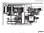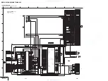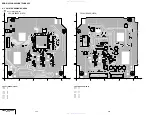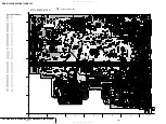
5-2
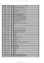
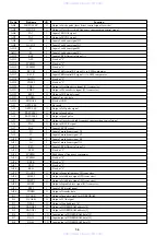
Pin No.
Pin Name
I/O
Function
51
52
53
54
55
56
57
58
59
60
61
62
63
64
65
66
67
68
69
70
71
72
73
74
75
76
77
78
79
80
81
82
83
84
94
95
96
97
98
99
100
FLCLK
RFTHRU
NC
FANCTL
VDD2
VSS2
P_CONT2
MUTECTL
EPGEQ
TUON
SWVION9V
P_CONT
FLON
SWVION5V
MRST
NC(IN)
CSYNCIN
XCHECKER
CEC
AVLIN
MSPSTAT
BLANK
HOTPLUG
TU_DCCON
TXD1
RXD1
TXD2
RXD2
HST_TO_M
VDDODA
CVBSIN
GND
FILTSLC
VDDVCO
LED_DIVX
LED_D_TV
LED_A_TV
LED_HDD2
DAT_TO_M
DAM_TO_T
ASCK
O
O
—
O
—
—
O
O
O
O
O
O
O
O
I
—
I
—
I
I
I
I
I
O
O
O
—
—
—
—
I
—
—
—
—
—
—
—
O
I
I
Output of clock signal for FLD driver
Output of tuner power supply control signal
Not used
Output of fan direction speed switching signal
Power supply input
Analog GND
Output of system power supply control signal
Output of SA mute control signal
Output of equalizer switching signal
Output of tuner block power supply control signal
Output of system power supply control signal
Output of switching regulator control signal
Output of FLD grid power supply on signal
Output of system power supply control signal
Input of system reset signal
Fixed at “L”
Input of C-synchronization/composite video signal
Not used
Input of blanking signal for euro scart
Output of tuner power supply control signal
Output of serial TXD signal [1] (Not used)
Output of serial RXD signal [1] (Not used)
Not used
Fixed at “L”
Not used
Not used
Input of composite video signal
Analog GND
Fixed at “L”
Power supply input
Not used
Output of system power supply control signal (Not used)
Fixed at “L”
Analog GND
Power supply input
Checking terminal
Checking terminal
Checking terminal
Not used
Not used
Not used
Not used
Not used
Output of serial data signal to ENC/DEC IC’s
Input of serial data signal from ENC/DEC IC’s
Input of serial clock signal from ENC/DEC IC’s
www. xiaoyu163. com
QQ 376315150
9
9
2
8
9
4
2
9
8
TEL 13942296513
9
9
2
8
9
4
2
9
8
0
5
1
5
1
3
6
7
3
Q
Q
TEL 13942296513 QQ 376315150 892498299
TEL 13942296513 QQ 376315150 892498299


