


SERVICE MANUAL
DVD RECORDER
SPECIFICATIONS
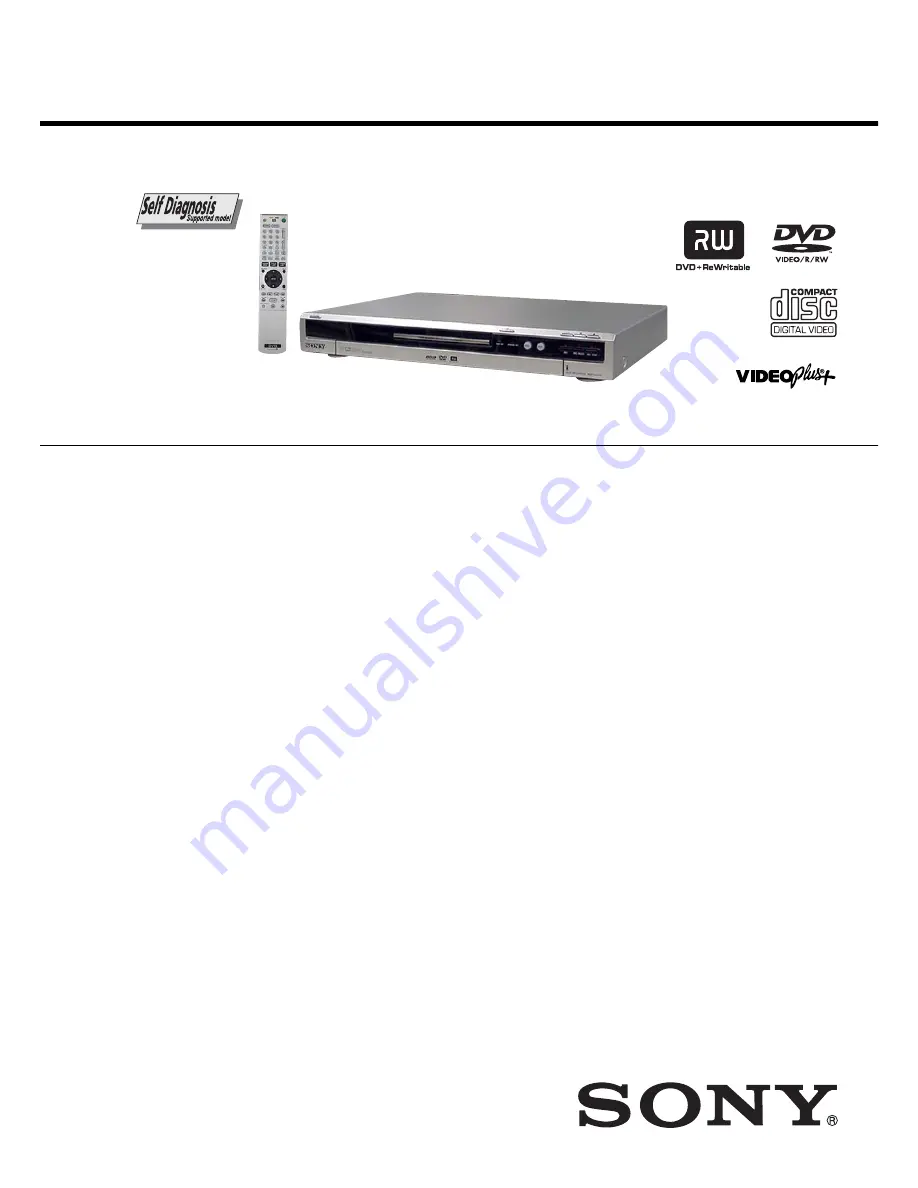
RDR-HX510
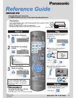
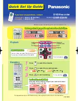
RMT-D217P
AEP Model
UK Model
System
Laser:
Semiconductor laser
Channel coverage:
PAL/SECAM (B/G, D/K, I, L)
VHF: E2 to E12, R1 to R12, F2 to F10, Italian
A to H, Ireland A to J, South Africa 4 to 13/
UHF: E21 to E69, R21 to R69, B21 to B69,
F21 to F69/CATV: S01 to S05, S1 to S20,
France B to Q/HYPER: S21 to S41
The above channel coverage merely ensures the
channel reception within these ranges. It does not
guarantee the ability to receive signals in all
circumstances.
Video reception:
Frequency synthesizer system
Audio reception:
Split carrier system
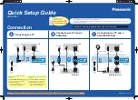
Aerial out:
75-ohm asymmetrical aerial socket
Timer:
Clock: Quartz locked/Timer indication:
24-hour cycle (digital)/Power back-up
duration: 1 hour
Video recording format:
MPEG Video
Audio recording format/applicable bit
rate:
Dolby Digital 2 ch/256 kbps
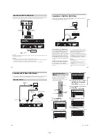
Inputs and outputs
LINE 2 OUT
(AUDIO):
Phono jack/2 Vrms/10 kilohms
(VIDEO):
Phono jack/1.0 Vp-p
(S VIDEO):
4-pin mini DIN/Y:1.0 Vp-p,
C: 0.3 Vp-p (PAL)
LINE 2 IN/LINE 4 IN
(AUDIO):
Phono jack/2 Vrms/more than
22 kilohms
(VIDEO):
Phono jack/1.0 Vp-p
(S VIDEO):
4-pin mini DIN/Y:1.0 Vp-p,
C: 0.3 Vp-p (PAL)
LINE 1 - TV :
21-pin
CVBS IN/OUT
S-Video/RGB OUT (upstream)
LINE 3/DECODER:
21-pin
CVBS IN/OUT
S-Video/RGB IN
S-Video OUT (downstream)
Decoder
DIGITAL OUT (OPTICAL):
Optical output jack/
–18 dBm (wave length: 660 nm)
DIGITAL OUT (COAXIAL):
Phono jack/
0.5 Vp-p/75 ohms
COMPONENT VIDEO OUT
(Y, P
B
/C
B
, P
R
/C
R
):
Phono jack/Y: 1.0 Vp-p, P
B
/C
B
: 0.7 Vp-p,
P
R
/C
R
: 0.7 Vp-p
General
Power requirements:
220-240 V AC,
50/60 Hz
Power consumption:
52 W
Dimensions (approx.):
430
×
65
×
328 mm
(width/height/depth) incl. projecting parts
Hard disk drive capacity:
80 GB
Mass (approx.):
4.8 kg
Operating temperature:
5
°
C to 35
°
C
Operating humidity:
25% to 80%
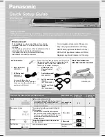
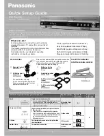
Supplied accessories:
Audio/video cord (1) (UK model only)
Mains lead (1)
Aerial cable (1)
Remote commander (remote) (1)
R6 (size AA) batteries (2)
Specifications and design are subject to change
without notice.
Compatible colour systems
This recorder is designed to record using the PAL
colour system and play back using the PAL or
NTSC colour systems.
The signals of the SECAM colour system can be
received or recorded but played back in the PAL
colour system only. Recording of video sources
based on other colour systems cannot be
guaranteed.
Summary of Contents for RDR-HX510
Page 6: ...MEMO 6 ...
Page 42: ...2 10E MEMO ...
Page 50: ...RDR HX510 MEMO 3 15 3 16E ...
Page 82: ...MEMO 5 4E ...