5-1
RDR-HX715
SECTION 5
IC PIN FUNCTION DESCRIPTION
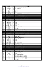
5-1. IT CONTROL IC (IC604: M306H3MC-058FPUO (AV-089 BOARD))
Pin No.
1
2
3
4
5
6
7
8
9
10
11
12
13
14
15
16
17
18
19
20
21
22
23
24
25
26
27
28
29
30
31
32
42
43
44
45
46
47
48
49
50
Pin Name
GRADE
SIRCS
AV_LINK_IN
FLD_DATA
FLD_IN
FLD_CLK
BYTE
CNVSS
XCIN
XCOUT
XRESET
XOUT
VSS
XIN
VCC
XNMI
SYNC_V
IT_REQ
SLICEON_IN
EUROPCONT
DIMMER
SH_P_CONT
BUZZER
STATUS0
RESET5V
STATUS1
AV_LINK_OUT
TU_SCL
TU_SDA
VSS2
LP2
LP3
TXT_SDA
TXT_SCL
STB_CNT
XAWAKE5
CLKOUT
AWAKE_DONE
XFLMRST
IT_XRST
FLD_XRESET
I/O
I
I
I
O
I
O
I
I
I
O
I
O
–
I
–
I
I
I
I
O
O
I/O
O
I
O
I
O
O
I/O
–
O
O
O
–
–
–
O
O
I
I
O
–
–
O
O
O
I
O
O
O
Function
Fixed at “L”
Remote control signal input
AV LINK signal input
Output of FLD data signal
Fixed at “L”
Output of FLD clock signal
Fixed at “L”
Connected to VCC when the FLASH is overwritten
Clock signal input (32.768KHz)
Clock signal output (32.768KHz)
System reset signal input
Clock signal output (10MHz)
GND
Clock signal input (10MHz)
Power supply input (5V)
Fixed at “H” (5V)
Detection of Vsync signal
Input of communication request signal with host IC
Input of slicer operation detection
Not used (Open)
Output of LED power supply switch
Not used
Not used
Status signal 0
Not used
Status signal 1
Not used (Open)
IIC clock signal output
IIC data signal input / output
GND
Filter output 2 (For Fsc)
Filter output 3 (For VPS)
Filter output 4 (For PDC)
Power supply input (5 V)
Fixed at “L”
Fixed at “L”
Output of slicer operation detection
Output of communication data with host IC
Input of communication data with host IC
Output of communication clock with host IC
Not used
Not used
Not used
Not used
Fixed at “L”
Input of wake-up state
Output of communication reset with Flash memory IC
Output of communication reset with host IC
Output of communication reset with FLD drive
www. xiaoyu163. com
QQ 376315150
9
9
2
8
9
4
2
9
8
TEL 13942296513
9
9
2
8
9
4
2
9
8
0
5
1
5
1
3
6
7
3
Q
Q
TEL 13942296513 QQ 376315150 892498299
TEL 13942296513 QQ 376315150 892498299

