— 25 —
•
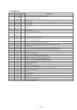
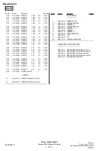
IC2 (µPD65012)
Pin No.
1 to 8
9 to11
12
13 to 20
21 to 28
29
30 to 32
33
34
35 to 38
39
40 to 42
43 to 50
51 to 52
53
54 to 59
60 to 63
64
65
66
67
68
69
70
71
72
73
74
75
76
77
78
79
80
I/O
I/O
I
—
I
I
I
—
—
I
I
O
I/O
O
—
O
O
O
O
O
O
O
O
O
—
—
O
O
O
I
I
I
O
I
Pin Function
Data transfer between µPD65012 and microprocessor.
Control input from microprocessor.
GND terminal.
Key scan input.
Key scan input.
Not used.
GND terminal.
Positive power supply terminal.
Not used.
Remote control signal received input.
External memory control output.
Data transfer between µPD65012 and external memory.
Terminals to which external memory is connected. Lower address (ADO to AD1)
GND terminal.
Terminals to which external memory is connected. Lower address (AD2 to AD7)
Terminals to which external memory is connected. Upper address (AD8 to AD11)
Not used.
Remote control signal output.
Remote control signal receiver block ON/OFF output.
SRAM IC3 (W24257S) ADD and IC8 (LH5359PA) ADD.
SRAM IC3 (W24257S) ADE and IC8 (LH5359PA) ADE.
Selector SRAM IC3 (W242575S) or ROM IC8 (LH5359PA)
EL control output. (Dark)
GND terminal.
Positive power supply terminal.
Terminals to which external memory is connected. Upper address. (AD12)
EL control output. (Bright).
Buzzer
GA reset input.
GA clock input.
Not used.
Microprocessor interrupt output.
Address latch enable input.
Pin Name
ID7 to ID0
IENN/IWIN
IRDN.
GND
IP30 to IP37
IP40 to IP47
KINT
IP50 to IP52
GND
V
DD
KINT
IP53 to IP56
REC
RDO.WTO
OCE
OD0 to OD7
AD0 to AD1
GND
AD2 to AD7
AD8 to AD11
OUTP
RMO
OP60
OP61
OP62
OP63
OP64
GND
V
DD
OP65
OP66
OP67
CLR
ICLK
RES
INT
IALE
Summary of Contents for RM-AV2000T
Page 3: ... 3 SECTION 1 GENERAL This section is extracted from instruction manual ...
Page 4: ... 4 ...
Page 5: ... 5 ...
Page 6: ... 6 ...
Page 7: ... 7 ...
Page 8: ... 8 ...
Page 9: ... 9 ...
Page 10: ... 10 ...
Page 11: ... 11 ...
Page 12: ... 12 ...
Page 13: ... 13 ...
Page 14: ... 14 ...

