11
11
RM-AX4000
RM-AX4000
SECTION 4
DIAGRAMS
Note on Schematic Diagrams:
• All capacitors are in
µ
F unless otherwise noted. (p: pF) 50 WV or
less are not indicated except for electrolytics and tantalums.
• All resistors are in
Ω
and
1
/
4
W or less unless otherwise specified.
•
f
: internal tolerance.
•
C
: panel designation.
•
A
: B+ Line.
• Voltages and waveforms are dc with respect to ground under no-
signal (detuned) conditions.
no mark : Power on
• Voltages are taken with a VOM (Input impedance 10 M
Ω
).
Voltage variations may be noted due to normal production toler-
ances.
• Waveforms are taken with a oscilloscope.
Voltage variations may be noted due to normal production toler-
ances.
• Circled numbers refer to waveforms.
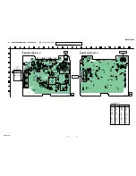
Note on Printed Wiring Boards:
•
Y
: parts extracted from the conductor side.
•
: Pattern from the side which enables seeing.
(The other layers' patterns are not indicated.)
Caution:
Pattern face side:
Parts on the pattern face side seen from
(Side B)
the pattern face are indicated.
Parts face side:
Parts on the parts face side seen from
(Side A)
the parts face are indicated.
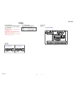
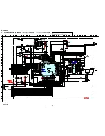
1
IC1
qg
(PI21/OSC-I)
2
IC1
qs
(PI23/OSC-I)
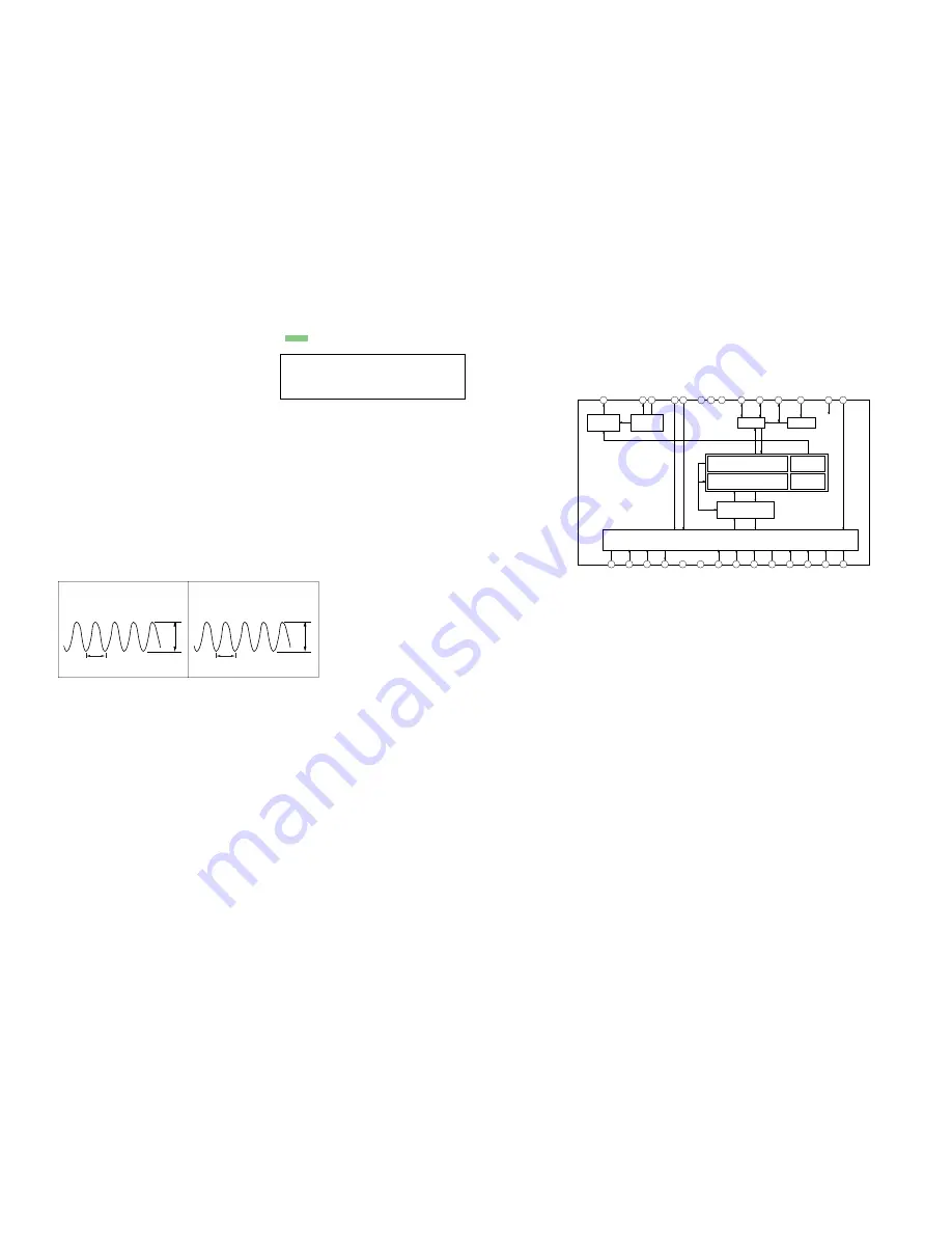
50.0 ns
2.6 Vp-p
1V/DIV, 40 ns/DIV
30.5us
3.7 Vp-p
1V/DIV, 10 us/DIV
• Waveforms
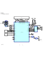
– MAIN Board –
MODE1_I
MODE0_I
XIN
XOUT
O_CLKKOUT
5
O_DRQ
6
DACK
VCC
GND
GND
D–
D+
AGND
RESET
D7
V3.3
24
23 22
21
28
27 26
25
20
19
17
16
15
18
Microcontroller Interface
1
I_CS
2
I_RD
3
I_WR/SK
4
O_INTR
24 MHz
Oscillator
Transceiver
VReg
Clock
Generator
Physical Layer Interface (PHY)
Media Access Controller (MAC)
Clock
Recovery
USB Event
Detect
Endpoint/Control FIFOs
7
I_AO/SLE/SI
8
O_DO/SO
9
D1
10
D2
11
D3
12
D4
13
D5
14
D6
Serial Interface Engine (SIE)
– MAIN Board –
IC2A USBN9604-28MXNOPB
• IC Block Diagram


