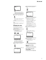

13
13
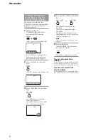
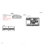
RM-AX4000
RM-AX4000
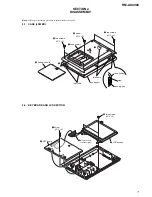
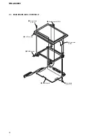
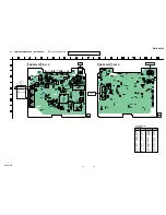
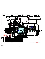
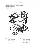
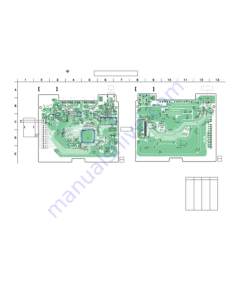
4-2. PRINTED WIRING BOARD – MAIN BOARD –
•
:Uses unleaded solder.
• Semiconductor
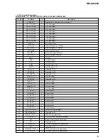
Location
Ref. No.
Location
D1
C-3
D2
A-8
D20
B-9
D21
E-5
D22
E-5
D23
E-5
D24
E-5
D40
D-9
IC1
D-5
IC3
C-3
IC4
D-3
IC6
B-4
IC2A
C-6
LED1
B3
Ref. No.
Location
LED2
B5
LED3
B-4
LED4
B-5
LED5
B-4
Q4
B-6
Q6
B-6
Q7
B-12
Q8
B-12
Q9
B-12
Q10
B-13
Q12
C-9
Q13
B-3
Q14
B-5
Q15
C-5
✩
IC1 (SYSTEM CONTROLLER) can not be replaced individually.
Replace it with MAIN board assembly for service.
IC3
IC6
IC1
IC2A
IC4
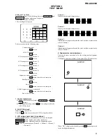
KEY BOARD
DRY BATTERY
SIZE "AA"
(IEC DESIGNATION R6)
4PCS. 6V
1-867-249-
11
VIN
VOUT
VSS
SEND
INFRARED RAYS
SEND
INFRARED RAYS
RECEIVED
INFRARED RAYS
MAIN BOARD
(SIDE A)
USB
1
5
1-867-248-
(11)
11
LCD UNIT
LCD UNIT
1-867-248-
(11)
11
1
4
MAIN BOARD
(SIDE B)