background image

S95E  Sony 


69


Summary of Contents for S95E

Page 1: ...S95E Sony 1 Service Manual TFT LCD COLOR COMPUTER DISPLAY SONY ...

Page 2: ...0 3 5 Service OSD 21 4 Disassembly flow chart 22 4 1 Disassembly steps 22 4 2 Wiring Diagram 26 4 3 Monitor Exploded View 27 5 Circuit principle analysis 28 5 1 Main board 28 5 1 1 Block diagram 28 5 1 2 Introduction of IC 29 5 1 3 Introduction of important function 26 5 2 PWPC board 31 5 2 1 Block diagram 31 5 2 2 Introduction of IC 32 5 2 3 Introduction of important function 33 6 Trouble shootin...

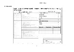
Page 3: ...S95E Sony 3 1 Precaution Warning on power connections Installation ...

Page 4: ...S95E Sony 4 Handing the LCD screen Maintenance Transportation ...

Page 5: ... LCD Panel Max dimension Horizontal 376 320mm Vertical 301 056mm R G B Analog 0 7Vp p R G B Digital TMDS H V separate TTL level 28kHz 80kHz Analog Horizontal frequency 28kHz 64kHz Digital 48 75Hz Analog Vertical rate 60Hz Digital Input signals Recommend resolution 1280 x 1024 60HZ Normal operation 50W Active off deep sleep 1W Power off 1W Power consumption Main power off 0W Power supply AC voltage...

Page 6: ...cription NO Description 1 Red Video 9 5V 2 Green Video Sync on Green 10 Sync Return 3 Blue Video 11 ID GND 4 ID GND 12 DDC Data 5 Sense of connection PC 13 Horizontal Sync 6 Red Video Return 14 Vertical Sync 7 Green Video Return 15 DDC Clock 8 Blue Video Return VGA Connector layout ...

Page 7: ...50 36 000 800 600 37 879 60 317 40 000 800 600 48 077 72 188 50 000 800 600 46 875 75 000 49 500 800 600 49 725 74 551 57 283 1024 768 48 363 60 004 65 000 1024 768 56 476 70 069 75 000 1024 768 60 023 75 029 78 750 1024 768 60 2 75 80 000 1152 864 67 5 75 108 000 1152 870 68 9 75 100 000 1152 900 61 8 66 92 940 1152 900 71 7 76 105 590 1170 584 31 2 50 46 200 1280 960 60 0 60 108 000 1280 1024 63...

Page 8: ...thin 2 seconds Besides Power Switch the picture and the green LED shall be lit When the Power button is pushed again the status shall be changed into Power Off within 1 second Besides the picture and the green LED shall disappear Menu Button OSD window shall be displayed by pressing the Menu button in the Power On condition Arrow Button These buttons are used to select the menu items make adjustme...

Page 9: ...l 4 Screen Adjust the picture s sharpness or its centering 5 Color Adjust the color temperature of the picture 6 γ Gamma Change the picture s color shade settings 7 Menu position Change the on screen menu position 8 Language Chance the language used on menus or messages 9 Reset Reset the adjustments to the default settings 10 Menu lock Lock the control of buttons to prevent accidental adjustments ...

Page 10: ...S95E Sony 10 Adjustment steps of each menu ...

Page 11: ...S95E Sony 11 ...

Page 12: ...S95E Sony 12 ...

Page 13: ...S95E Sony 13 ...

Page 14: ...S95E Sony 14 ...

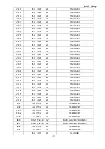
Page 15: ...S95E Sony 15 ...

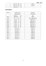
Page 16: ...S95E Sony 16 ...

Page 17: ...S95E Sony 17 ...

Page 18: ...S95E Sony 18 ...

Page 19: ...S95E Sony 19 ...

Page 20: ... for more than 30 minutes for RGB reset before W B adjustment 2 Setup 1 Prepare timing and pattern data for a signal generator according to the Sony timing specifications 2 Connect a monitor video cable to the signal generator 3 Put Color Analyzer ex CA 110 50cm away from the monitor specify it vertically in the center of the display and adjust the focus to the optimum level using an eyepiece 4 Pu...

Page 21: ... Repeat the adjustment procedure as steps b to d at 9300K 3 5 Service OSD To enter service OSD menu 1 Turn off the power switch button 2 Press volume down and then power key 3 Shows the service OSD menu That menu is located in down side of main menu 4 The service OSD menu contains additional menus as described below a ADC CALBRATION Adjust the offset voltage and gain value in PC mode b VIDEO CALBR...

Page 22: ...ce of clean cloth mat under it for preventing scratching the panel 2 Be careful when open the bezel and rear cover with the tool that mentioned above for preventing mangling them 3 Put away the screws for preventing rolling on the panel and scratching it 4 Be careful and don t scratch the connection line when open the shield 5 Press the interface with a hand and pull or insert the connection line ...

Page 23: ...ny 23 Step2 Figure Description Discharge the base 1 Wring the five screws in the bracket marked in red 2 Take the screw and stand away 3 Steel line marked in green is to rise or lower the stand Wring the screw ...

Page 24: ...ip with the other then move it in the forward hour hand 3 Pay attention to some hooks then open it with little force till the bezel and rear cover separated 4 The position marked with arrows exists some hooks 5 After bezel and rear cover separated the bezel is shown in the figure down left Discharge the rear cover shield 1 Wring down the screw in the shield which is marked in red ...

Page 25: ...s marked in red 2 Pull out the lamp and main board connection lines marked in yellow Discharge the main board 1 Wring the four screws marked with red 2 Pull out the other connection lines marked in yellow Discharge the panel Wring down the four screws marked in red A ...

Page 26: ...S95E Sony 26 The panel is disassembled absolutely 4 2 WIRING DIAGRAM ...

Page 27: ...S95E Sony 27 4 3 Monitor Exploded View ...

Page 28: ...logic brightness control logic and DDC 5 1 Main board 5 1 1 Block diagram The main board contains panel control logic brightness control logic DDC and DC convert DC circuit and so on Main board PWPC board Video signal and DDC Key board Backlight and Panel HOST computer R G B H V SDA SCL GM5321 OSC Backlight and Panel PWPC board EPROM EPROM Keyboard ...

Page 29: ...rt used to 5v convert 3 3v AIC1084 18CE DC power convert used to 5v convert 1 8v 5 1 3 Introduction of important function DC TO DC The required power supply are different for each chip and the voltage of 12v 5v offered by PWPC can t reach the requirement so we deal with this problem by means of two pieces of DC TO DC chips AIC1084 18CM AIC1084 33CM The circuit diagrams are as follows ...

Page 30: ... when it s saving energy state and Q402 break off Q203 break off so the panel doesn t work On Off Brightness control circuit ON OFF control When it works well the high level output form PIN 68 of U201 and low in saving energy state Brightness control When it works well the output PWM pulse from PIN98 of U201 adjusts the brightness the bigger the duty and the higher the brightness ...

Page 31: ...ply for each chips in the main board and inverter Inverter is DC TO AC circuit It changes the 12v DC of power supply to about 600 800v AC that drives the backlight It mostly consists of starting circuit PWM controller DC changing circuit LC surging circuit output circuit and protection circuit etc Interface of main board and PWPC board EMI filter Bridge Rectifier Start Circuit R904 R908 PWM Contro...

Page 32: ... Control Pin Error amplifier and feedback current input pin for duty cycle control 2 L Line Sense Pin Input pin for OV UV line feed forward with DCMAX reduction remote ON OFF and synchronization 3 X External Current Limit Pin Input pin for external current limit adjustment remote ON OFF and synchronization 4 S Source Pin Output MOSFET source connection for high voltage power return 5 F Frequency P...

Page 33: ...er 6 1DTC Output 1 dead time soft start setting 14 2IN Positive input for error amplifier 7 1OUT Output 1 15 SCP Timing latch setting 8 GND Ground 16 REF Reference voltage output 2 5v 5 2 3 Introduction of important function a Adapter EMI filter circuit It is common used to get rid of the disturbance existing in the electric net or coming from outside L901 is used to reduce the symmetry disturbanc...

Page 34: ...ed voltage is supplied to L Pin of IC901 TOP247Y The output pulse makes T901 work The voltage produced at the two terminals of T901 is offered to C Pin of IC901 after being commuted by D905 and filtered by C914 and then the whole start up process is end Over voltage Protection circuit 1 ZD903 can be broken down when12V DC voltage increases which leads to the current increase through IC902 and volt...

Page 35: ...filter output circuit When D Pin of IC901 has pulse output which makes T901 work while being given a low level and there is a current in the primary coil of T901 with a voltage up terminal positive and down negative so the secondary coil produces a reverse electromotive force It is the stage of storing energy in the coil because D902 D904 are closed But while being given a high C Pin of IC901 ...

Page 36: ...Pin 98 of U201 in the main board with its range of 0 5V The Inverter offers different currents to the loads because of the different feedback of voltage to the feedback terminal of PWM The smaller the value of DIM the smaller the current output of Inverter the darker the brightness Voltage start up circuit It consists of a PNP and a NPN transistor with two working stages The first stage When the O...

Page 37: ...nloaded it also means that there is no feedback voltage applied to PIN14 and PIN3 of U201 the inside circuit will work to protect the circuit DC DC Circuit The DC DC Circuit is made up of MOSFET Q203 energy storing inductor L201 and D201 The pulse output of BA9741A is magnified by the amplifier made up of Q205 Q207 to drive the MOSFET It performs charge to L201 when the high level coming thus the ...

Page 38: ...ling C215 C216 C232 are coupling capacitance for voltage division as output The two terminals of capacitance is applied across a certain voltage because of the impedance exists in capacitor The voltage across the backlight can decay to about 800V by selecting the parameter value of capacitance Feedback circuit Alternating voltage exists at the two terminals of R232 when the loads are working After...

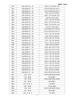
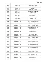
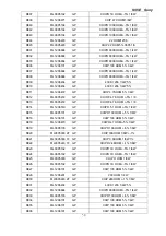
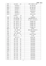
Page 39: ...S95E Sony 39 ...

Page 40: ...k if the picture is normal OK Please reinsert and make sure the AC of 100 240 is normal Measure U602 PIN2 3 3V C609 1 8V Reinsert or check the power section X301 oscillate waveforms are normal Check Correspondent component OK OK OK NG NG NG Replace U301 Check Correspondent component OK NG ...

Page 41: ...S95E Sony 41 No picture LED orange No picture Measure U602 PIN2 3 3V C609 1 8 Check Correspondent component Replace U301 X301 oscillate waveform is normal Check Correspondent component OK OK NG NG ...

Page 42: ...502 base is high level Measure U602 PIN2 3 3V C609 1 8V X301 oscillate waveform is normal Check Q502 and Q501 are broken or CN501 solder Check Correspondent component Check Correspondent component Replace U301 OK OK OK Check Correspondent component OK NG NG NG NG ...

Page 43: ... or 240V NG OK Change F901 check BD901 Q903 IC901 Check the voltage of C905 Check bridge rectified circuit NG OK Check start voltage for the pin3 of IC901 Change IC901 NG Repeating the start voltage Check the auxiliary voltage is smaller than 24V 1 Check IC902 IC903 2 Check Q901 Q902 OVP circuit NG OK Check R904 D902 D904 ZD903 OK ...

Page 44: ...V_D pin11 PDRV C pin12 PDRV A pin19 NDRV B pin20 of IC801 Check full bridge power conversion circuit and Transformer output circuit OK NG Change IC801 OK OK Check FB pin9 of IC801 and Protection loop debug and connect b pin of Q802 Q803 to GND Judge FB 0 OK Check FB circuit form lamp s return to FB pin9 of IC801 NG Normal condition Check b pin voltage of Q802 Q803 0V OK End FB circuit and Protecti...

Page 45: ...LO B GP REAR COVER 40G 152509 GP RECYCLE LABEL 40G 152512 GP RECYCLE LABEL 40G 457834 4A GP S N LABEL FOR ID 40G 457834 9A GP CARTON LABEL 40G 58162435A GP LABEL FOR PE BAG 44G6002834 9A GP PAPER PLATE 44GP902 1 GP PULP MOLD 44GP902 2 GP PULP MOLD 44GP902624 1A CARTON 45G 88607SY1 GP EPE BAG FOR MONITOR 45G 88621 21 GP PE RING 50G 600 2 HANDLE1 50G 600 3 HANDLE2 52G 1185 GP MIDDLE TAPE FOR CARTON ...

Page 46: ...rt NO for TPV Description 33G4878 LO L GP HOLDER AUDIO OUT 95G8014 3 14 GP AUDIO 3 3 WIRE HARNESS 715G1519 1 GP PCB CN801 33G3802 3H GP S3D PH K S LF SN TST CN802 88G 30226T GP PHONE JACK 3 5MM 3P C1F CN802 88G 30226T TO GP PHONE JACK 3 5MM CBPC982KAD1SP Symbol Part NO for TPV Description AIC982KAD1SP MAIN BOARD 15G8170 1 GP BKT CONNECTOR 40G 457624 1B GP CPU LABEL 40G 45762420A GP CBPC LABEL 25X6...

Page 47: ... K S LF SN TST L602 73G 253158 L INUDCTOR 15UH PE 54041S U301 90G6077 2 GP HEAT SINK X301 93G 22 53 CRYSTAL 14 318MHzHC 49U 715G1506 1 GP PCB main board C201 65G0603104 12 GP CHIP 0 1UF 16V X7R C212 65G0603104 12 GP CHIP 0 1UF 16V X7R C213 65G0603104 12 GP CHIP 0 1UF 16V X7R C214 65G0603103 32 GP CHIP 0 01UF 50V X7R C215 65G0603103 32 GP CHIP 0 01UF 50V X7R C217 65G0603103 32 GP CHIP 0 01UF 50V X7...

Page 48: ...NPO C330 65G0603104 12 GP CHIP 0 1UF 16V X7R C331 65G0603104 12 GP CHIP 0 1UF 16V X7R C332 65G0603104 12 GP CHIP 0 1UF 16V X7R C333 65G0603104 12 GP CHIP 0 1UF 16V X7R C401 65G0603104 32 GP CHIP 0 1UF 50V X7R C402 65G0603102 32 GP 1000PF 10 50V X7R C403 65G0603102 32 GP 1000PF 10 50V X7R C404 65G0603102 32 GP 1000PF 10 50V X7R C405 65G0603102 32 GP 1000PF 10 50V X7R C407 65G0603102 32 GP 1000PF 10...

Page 49: ...33 DIO SIG SM BAV99 PHSE D702 93G 64 33 DIO SIG SM BAV99 PHSE D705 93G 64 33 DIO SIG SM BAV99 PHSE D706 93G 64 33 DIO SIG SM BAV99 PHSE FB201 71G 59C800 GP CHIP BEAD FB202 71G 59C800 GP CHIP BEAD FB203 71G 59C800 GP CHIP BEAD FB301 71G 56K121 GP GA 120 OHM BEAD FB301 71G 56K121 M GP 120 OHM 6A FB302 71G 56K121 GP GA 120 OHM BEAD FB302 71G 56K121 M GP 120 OHM 6A FB303 71G 56K121 GP GA 120 OHM BEAD ...

Page 50: ...CHIPR 100 OHM 5 1 10 R231 61L0603101 GP CHIPR 100 OHM 5 1 10 R232 61L0603101 GP CHIPR 100 OHM 5 1 10 R234 61L0603101 GP CHIPR 100 OHM 5 1 10 R235 61L0603750 GP CHIPR 75 OHM 5 1 10W R236 61L0603750 GP CHIPR 75 OHM 5 1 10W R237 61L0603750 GP CHIPR 75 OHM 5 1 10W R238 61L0603330 1F GP CHIPR 3 3K OHM 1 1 1 R241 61L0603100 2F GP CHIPR 10K OHM 1 1 10 R243 61L0603472 GP CHIPR 4 7K OHM 5 1 1 R244 61L06032...

Page 51: ...OHM 5 1 10 R405 61L0603472 GP CHIPR 4 7K OHM 5 1 1 R406 61L0603103 GP CHIPR 10K OHM 5 1 10 R408 61L0603303 GP CHIP 30K OHM 5 1 10W R409 61L0603473 GP CHIP 47K OHM 1 10W R410 61L0603223 GP CHIP 22KOHM 1 16W R411 61L0603303 GP CHIP 30K OHM 5 1 10W R413 61L0603472 GP CHIPR 4 7K OHM 5 1 1 R414 61L0603392 GP CHIP 3 9K OHM 1 10W R415 61L0603472 GP CHIPR 4 7K OHM 5 1 1 R502 61L1206331 GP CHIP 330 OHM 5 R...

Page 52: ...3 59AS3 SST25VF010 20 4C SAE SO U601 56G 133 32 NS LM3485 MSOP 8 NS U602 56G 563 7 AIC1084 33PM ZD207 93G 39S 34 T UDZS5 6B ZD208 93G 39S 34 T UDZS5 6B ZD210 93G 39S 34 T UDZS5 6B ZD212 93G 39S 34 T UDZS5 6B ZD213 93G 39S 34 T UDZS5 6B ZD216 93G 39S 34 T UDZS5 6B ZD301 93G 39S 34 T UDZS5 6B ZD401 93G 39S 34 T UDZS5 6B ZD402 93G 39S 34 T UDZS5 6B ZD403 93G 39S 34 T UDZS5 6B ZD404 93G 39S 34 T UDZS5...

Page 53: ... 67G215S10115N GP EC CAP 450V 100 C905 67G215S10115Q GP LOWESR EC 100UF 450V UP C906 67G215L471 4Q GP LOW ESR EC 470UF 25V UH C906 67G215V471 4N GP KY25VB470M CC3 10 16 C908 67G215L471 4Q GP LOW ESR EC 470UF 25V UH C908 67G215V471 4N GP KY25VB470M CC3 10 16 C909 67G215L471 4Q GP LOW ESR EC 470UF 25V UH C909 67G215V471 4N GP KY25VB470M CC3 10 16 C911 67G215L471 4Q GP LOW ESR EC 470UF 25V UH C911 67...

Page 54: ... CERAMIC CAP C843 65G 3J1006EM GP 10PF 5 SL 3KV MURATA C843 65L 3J1006ET GP 10PF 5 SL 3KV TDK C844 65G 3J1006EM GP 10PF 5 SL 3KV MURATA C844 65L 3J1006ET GP 10PF 5 SL 3KV TDK C901 65G306M1022BM GP Y1 CAP 001UF 250VAC MUR C902 65G306M1022BM GP Y1 CAP 001UF 250VAC MUR C903 63G 10747410S GP 0 47UF 10 250VAC C921 65G306M1022BM GP Y1 CAP 001UF 250VAC MUR FB901 71G 55 29 GP FERRITE BEAD VAR901 61G 46 12...

Page 55: ...P 0 1UF 10 25V X7R 080 C838 65G0805104 22 GP 0 1UF 10 25V X7R 080 C839 65G0805105 22 GP CHIP 1UF 25V X7R 0805 C841 65G1206225 17 GP CHIP 2 2UF 16V Y5V 1206 C846 65G1206225 17 GP CHIP 2 2UF 16V Y5V 1206 C847 65G1206225 17 GP CHIP 2 2UF 16V Y5V 1206 C848 65G0805104 22 GP 0 1UF 10 25V X7R 080 C907 65G0805104 22 GP 0 1UF 10 25V X7R 080 C910 65G0805104 22 GP 0 1UF 10 25V X7R 080 C914 65G1206104 32 GP C...

Page 56: ...JR805 61L1206000 GP CHIPR 0 OHM 5 1 4W JR806 61L1206000 GP CHIPR 0 OHM 5 1 4W JR807 61L1206000 GP CHIPR 0 OHM 5 1 4W JR901 61L1206000 GP CHIPR 0 OHM 5 1 4W JR902 61L1206000 GP CHIPR 0 OHM 5 1 4W Q802 57G 417 4 PMBS3904 PHILIPS SMT 04 Q802 57G 417 4A 2SC3052 T112 1F Q803 57G 417 4 PMBS3904 PHILIPS SMT 04 Q803 57G 417 4A 2SC3052 T112 1F Q806 57G 760 4 DTA144WKA BY ROHM SMT Q806 57G 760 4B PDTA144WK ...

Page 57: ...105 GP CHIP IMOHM 0805 R808 61L0805362 GP CHIP 3 6KOHM 0805 R809 61L0805200 2F GP CHIP 20KOHM 1 8W R811 61L0805513 GP CHIP 51 KOHM 0805 R812 61L0805333 GP CHIP 33K OHM 0805 R814 61L0805300 2F GP CHIPR 30KOHM 1 1 8W R816 61L0805102 GP CHIPR 1K OHM 5 1 8W R817 61L0805105 GP CHIP IMOHM 0805 R818 61L0805102 GP CHIPR 1K OHM 5 1 8W R819 61L0805270 0F GP CHIPR 270 OHM 1 1 8W R820 61L0805362 GP CHIP 3 6KO...

Page 58: ...OHM 5 1 8 R913 61L0805472 GP CHIRP 4 7K OHM 5 1 8 R914 61L1206519 GP CHIPR 5 1 OHM 5 1 4W R915 61L0805101 GP CHIPR 100 OHM 5 1 8W R916 61L1206101 GP CHIP 100 OHM 5 1 4W R918 61L1206470 GP CHIPR 47 OHM 5 1 4W R919 61L0805103 GP CHIPR 10K OHM 5 1 8W R920 61L0805330 2F GP CHIP 33KOHM 1 8W 1 R921 61L0805360 1F GP CHIP 3 6KOHM 1 8W 1 R922 61L0805240 1F GP CHIPR 2 4KOHM 1 1 8W R923 61L0805102 GP CHIPR 1...

Page 59: ...K152 1T GP CERAMIC CAP C934 65G 2K152 1T GP CERAMIC CAP CN901 6G 31500 GP EYELET D901 93G 6026T52T RECTIFIER DIODE FR107 D902 6G 31502 GP 1 5MM RIVET D905 93G 6038T52T FR103 F901 84G 55 7 GP FUSE 3 15A 250V IC903 56G 158 4 T A H431BA IC903 56G 158 10 T AZ431AZ AE1 JP801 95G 90 23 GP TIN COATED JP802 95G 90 23 GP TIN COATED JP803 95G 90 23 GP TIN COATED JP804 95G 90 23 GP TIN COATED JP805 95G 90 23...

Page 60: ...5G 90 23 GP TIN COATED JP905 95G 90 23 GP TIN COATED JP906 95G 90 23 GP TIN COATED JP908 95G 90 23 GP TIN COATED JP909 95G 90 23 GP TIN COATED JP910 95G 90 23 GP TIN COATED JP911 95G 90 23 GP TIN COATED JP912 95G 90 23 GP TIN COATED JP913 95G 90 23 GP TIN COATED JP914 95G 90 23 GP TIN COATED JP915 95G 90 23 GP TIN COATED JP917 95G 90 23 GP TIN COATED JP918 95G 90 23 GP TIN COATED L901 6G 31502 GP ...

Page 61: ...P SHRINK TUBE UL CSA R904 61G152M39858F GP 0 39 OHM 5 2W 95G 90 23 GP TIN COATED 96G 29 1 GP SHRINK TUBE UL CSA KEPC982KS2P KEY BOARD 1G6017 1 GP THUMB SCREW 12G6088 1 GP BASE BUBBER FOOT 15G8180 1 GP BKT BASE UPPER 15G8181 1 GP BKT BASE LOWER 15G8243 1 GP BKT VESA 33G4877 RT L GP BUTTON 33G4879 OD L GP LENS 33G4883 1 X GP RINGE SWIVEL 34G1585APY B GP BEZEL 34G1598 LO B GP STAND COVER F 34G1599 LO...

Page 62: ...TRB SW101 77G 605 1 AL GP SMD SWITCH SW102 77G 605 1 AL GP SMD SWITCH SW103 77G 605 1 AL GP SMD SWITCH SW104 77G 605 1 AL GP SMD SWITCH SW105 77G 605 1 AL GP SMD SWITCH SW106 77G 605 1 AL GP SMD SWITCH ZD101 93G 39S 34 T UDZS5 6B ZD102 93G 39S 34 T UDZS5 6B ZD103 93G 39S 34 T UDZS5 6B ZD104 93G 39S 34 T UDZS5 6B ZD105 93G 39S 34 T UDZS5 6B ZD106 93G 39S 34 T UDZS5 6B ZD107 93G 39S 34 T UDZS5 6B ZD...

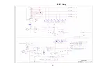
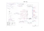
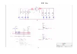
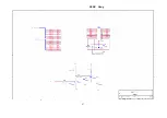
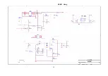
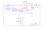
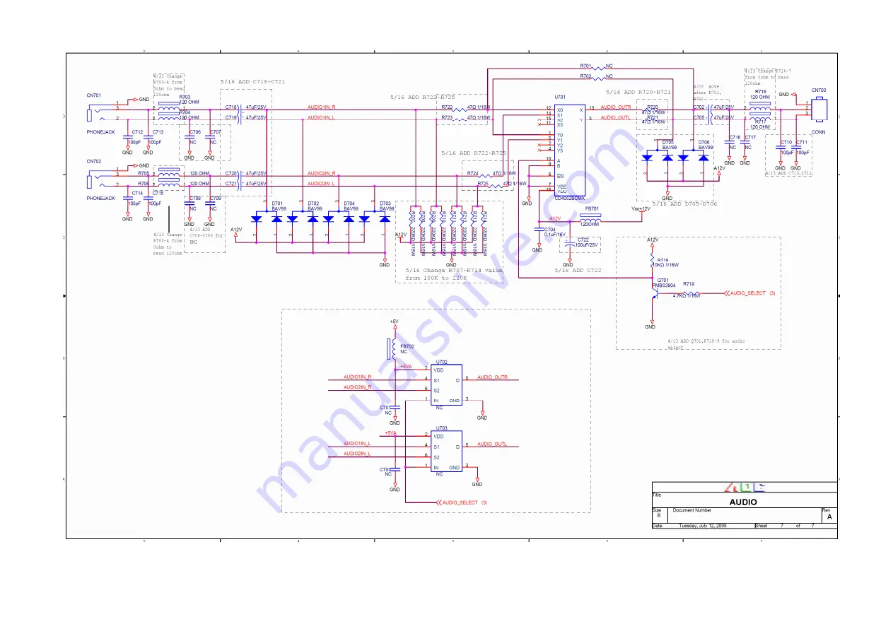
Page 63: ...S95E Sony 63 8 Schematic ...

Page 64: ...S95E Sony 64 ...

Page 65: ...S95E Sony 65 ...

Page 66: ...S95E Sony 66 ...

Page 67: ...S95E Sony 67 ...

Page 68: ...S95E Sony 68 ...

Page 69: ...S95E Sony 69 ...

Reviews: