49
•
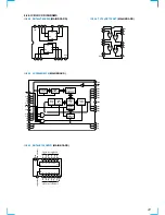
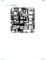
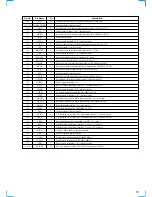
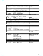
MAIN BOARD IC701 CXD1882R
(SACD DECODER)
Pin No.
1, 2
3
4
5
6
7
8
9 to 14
15
16
17
18
19
20, 21
22
23
24
25
26
27
28
29
30
31
32
33
34
35
36
37
38
39
40
41
42
43
44
45
46
47
48
49
50
51
52
53
54
55
56
57
58
59, 60
I/O
I/O
—
I/O
I
—
I
—
I
—
O
I
I
I
O
—
I
O
—
O
O
—
O
O
O
O
—
O
O
—
O
—
O
O
O
—
O
O
O
O
—
O
O
—
O
—
I
O
O
I
I/O
—
I
Description
Two-way data bus with the CPU (IC901) and expander (IC902)
Ground terminal (digital system)
Two-way data bus with the CPU (IC901) and expander (IC902)
Address signal input from the CPU (IC901)
Power supply terminal (+3.3V) (digital system)
Address signal input from the CPU (IC901)
Power supply terminal (+5V)
Address signal input from the CPU (IC901)
Ground terminal (digital system)
Wait signal output terminal Not used (open)
Read strobe signal input from the CPU (IC901)
Write strobe signal input from the CPU (IC901)
Chip select signal input from the CPU (IC901)
Interrupt signal output to the CPU (IC901)
Power supply terminal (+3.3V) (digital system)
Not used (open)
Stream data signal output to the DSD decoder (IC801)
Ground terminal (digital system)
Error flag signal output to the DSD decoder (IC801)
Stream data signal output to the DSD decoder (IC801)
Power supply terminal (+5V) (digital system)
Not used (open)
Stream data signal output to the DSD decoder (IC801)
Not used (open)
Stream data signal output to the DSD decoder (IC801)
Ground terminal (digital system)
Not used (open)
Stream data signal output to the DSD decoder (IC801)
Power supply terminal (+3.3V) (digital system)
Not used (open)
Power supply terminal (+5V) (digital system)
Stream data signal output to the DSD decoder (IC801)
Not used (open)
Stream data signal output to the DSD decoder (IC801)
Ground terminal (digital system)
Not used (open)
Stream data signal output to the DSD decoder (IC801)
Not used (open)
Serial data transfer acknowledge signal output to the DSD decoder (IC801)
Power supply terminal (+5V) (digital system)
Serial data transfer clock signal output to the DSD decoder (IC801)
Header flag signal output to the DSD decoder (IC801)
Power supply terminal (+3.3V) (digital system)
Not used (pull up)
Ground terminal (digital system)
Serial data transfer request signal input from the DSD decoder (IC801)
Not used (pull up)
Not used (pull up)
Not used (fixed at “H” )
Not used (pull up)
Power supply terminal (+5V) (digital system)
Not used (fixed at “H” )
Pin Name
D5, D6
VSS
D7
A0
VDD
A1
VDD5V
A2 to A7
VSS
XWAIT
XRD
XWR
XCS
XINT0, XINT1
VDD
XHRS
HDB7
VSS
HDB8
HDB6
VDDS
HDB9
HDB5
HDBA
HDB4
VSS
HDBB
HDB3
VDD
HDBC
VDDS
HDB2
HDBD
HDB1
VSS
HDBE
HDB0
HDBF
XACK
VDDS
DCK
XSHDR0
VDD
REDY
VSS
REQUEST
HINT
XS16
HA1
XPDI
VDDS
HA0, HA2
Summary of Contents for SCD-C333ES - Super Audio Cd Changer
Page 18: ...SCD C333ES 18 18 4 2 SCHEMATIC DIAGRAM RF SECTION Refer to page 40 for Waveforms ...
Page 28: ...SCD C333ES 28 28 4 12 SCHEMATIC DIAGRAM AUDIO SECTION 2 3 ...
Page 29: ...SCD C333ES 29 29 4 13 SCHEMATIC DIAGRAM AUDIO SECTION 3 3 ...
Page 34: ...SCD C333ES 34 34 4 18 SCHEMATIC DIAGRAM HP SECTION ...
Page 36: ...SCD C333ES 36 36 4 20 SCHEMATIC DIAGRAM SENSOR SECTION Refer to page 45 for IC Block Diagram ...
Page 38: ...SCD C333ES 38 38 4 22 SCHEMATIC DIAGRAM POWER SECTION ...

