background image

SERVICE MANUAL

SPECIFICATIONS

SDM-P82

TFT LCD Color Computer Display

US Model

Canadian Model

LCD panel

Panel type: a-Si TFT Active Matrix
Picture size: 18.1 inch

Input signal format

RGB operating frequency*
Horizontal: 28 – 92 kHz
Vertical: 56 – 85 Hz

Resolution

Horizontal: Max.1280 dots
Vertical: Max.1024 lines

Input signal levels

Analog RGB video signal

0.7 Vp-p, 75

, positive

SYNC signal

TTL level, 2.2 k

,

positive or negative
(Separate horizontal and vertical,
or composite sync)
0.3 Vp-p, 75

, negative

(Sync on green)

Digital RGB (DVI) signal: TMDS
(Single link)

Power requirements

100 – 240 V, 50 – 60 Hz,
Max. 1.2 A

Power consumption

Max. 58 W

Operating temperature

5 – 35

°

C

Dimensions (width/height/depth)

Display (upright):

Approx. 404

×

406

×

201 mm

(16

×

16

×

8 inches)

(with stand)
Approx. 404

×

332.6

×

86.2 mm

(16

×

13

1

/

8

×

3

1

/

2

inches)

(without stand)

Mass

Approx. 7.6 kg (16 lb 12 oz) (with
stand)
Approx. 6.3 kg (13 lb 14 oz)
(without stand)

Plug & Play

DDC2B

* Recommended horizontal and vertical timing condition

• Horizontal sync width duty should be more than 4.8% of total

horizontal time or 0.8

µ

s, whichever is larger.

• Horizontal blanking width should be more than 2.5

µ

sec.

• Vertical blanking width should be more than 450

µ

sec.

Design and specifications are subject to change without notice.

Summary of Contents for SDM-P82

Page 1: ...GB DVI signal TMDS Single link Power requirements 100 240 V 50 60 Hz Max 1 2 A Power consumption Max 58 W Operating temperature 5 35 C Dimensions width height depth Display upright Approx 404 406 201 mm 16 16 8 inches with stand Approx 404 332 6 86 2 mm 16 13 1 8 3 1 2 inches without stand Mass Approx 7 6 kg 16 lb 12 oz with stand Approx 6 3 kg 13 lb 14 oz without stand Plug Play DDC2B Recommended...

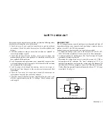
Page 2: ...ore releasing the set to the customer 1 Check the area of your repair for unsoldered or poorly soldered connections Check the entire board surface for solder splashes and bridges 2 Check the interboard wiring to ensure that no wires are pinched or contact high wattage resistors 3 Check that all control knobs shields covers ground straps and mounting hardware have been replaced Be absolutely certai...

Page 3: ...TIFIED IN THIS MANUAL FOLLOW THESE PROCEDURES WHENEVER CRITICAL COMPONENTS ARE REPLACED OR IM PROPER OPERATION IS SUSPECTED AVERTISSEMENT ATTENTION AUX COMPOSANTS RELATIFS À LA SÉCURITÉ LES COMPOSANTS IDENTIFIÉS PAR UNE TRAME ET UNE MARQUE SONT CRITIQUES POUR LA SÉCURITÉ NE LES REMPLACER QUE PAR UNE PIÈCE PORTANT LE NUMÉRO SPECIFIÉ LES RÉGLAGES DE CIRCUIT DONT L IMPORTANCE EST CRITIQUE POUR LA SÉC...

Page 4: ...ry to provide a high quality picture at the center of the screen If the input signal matches the factory preset mode the picture is appears on the screen automatically with the appropriate default adjustment If input signals do not match one of the factory preset modes When the monitor receives an input signal the automatic picture quality adjustment function of this monitor is activated and ensur...

Page 5: ...s of Service Mode 2 3 2 4 White Balance Adjustment 2 3 2 5 Action after Replacing the LCD Panel and Board 2 5 TABLE OF CONTENTS Section Title Page Section Title Page 3 DIAGRAMS 3 1 Block Diagrams 3 1 3 2 Circuit Boards Location 3 2 3 3 Schematic Diagrams and Printed Wiring Boards 3 2 1 Schematic Diagram of A a b c d e f g Board 3 4 2 Schematic Diagram of H Board 3 12 3 Schematic Diagram of I Board...

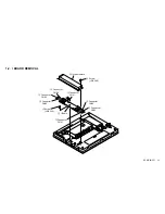
Page 6: ...SDM P82 UC 1 1 SECTION 1 DISASSEMBLY 1 1 REAR COVER AND CABINET ASSY REMOVAL 2 Rear cover 4 Cabinet assy Protechtion sheet 1 Connector cover 3 Two screws PSW 4X8 3 Two screws PSW 4X8 ...

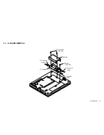
Page 7: ...82 UC 1 2 1 2 I BOARD REMOVAL 5 I Board 1 Screw RK 3X6 4 Screw RK 3X6 2 Invertor shield 3 Connector CN06 3 Connector CN05 3 Connector CN07 3 Connector CN02 3 Connector CN03 3 Connector CN04 3 Connector CN01 ...

Page 8: ...SDM P82 UC 1 3 1 3 G BOARD REMOVAL 4 Screw RK 3X6 1 Two crews RK 3X6 3 Connector CN102 3 Connector CN203 3 Connector CN101 5 G Board 2 Shield ...

Page 9: ...4 A BOARD REMOVAL 3 Interface shield 5 Frexible cable 1 Screw RK 3X6 2 Three screws PWH 3X6 6 Four screws PWH 3X6 5 Connector CN304 5 Connector CN201 5 Connector CN202 4 Six connector screws 5 Connector CN501 7 A board ...

Page 10: ...SDM P82 UC 1 5 1 5 LCD UNIT REMOVAL 1 Flexible cable 2 Two screws K 2X4 2 Beznet assy 2 Two screws K 2X4 3 LCD unit ...

Page 11: ...SDM P82 UC 1 6 1 6 LCD PANEL REMOVAL 2 LCD panel 1 Two screws PWH 3X6 1 Two screws PWH 3X6 ...

Page 12: ...SDM P82 UC 1 7 1 7 H BOARD REMOVAL 1 Switch cover 3 Connector CN901 2 Flexible cable 3 H Board ...

Page 13: ...setting when the input with no input signal is selected the system goes into the AGING MODE The NO SYNC AGING flag is held until it is cleared To clear the NO SYNC AGING flag go into the service mode and then set the AGING MODE to OFF or execute the all mode recall 5 To enter the service mode Press the POWER button with pressing the UP and DOWN buttons in the power off state and the system is set ...

Page 14: ... main menu with the UP or DOWN button then select the MAINTAIN icon on the bottom line and then press the OK button 4 In this menu screen the version number and released date of the internal software can be checked 5 The structure of the MAINTAIN menu is shown below The operation procedure is basically same as that of the ordinary user controls The function of each menu is explained in next sectio...

Page 15: ... held until it is cleared To clear the NO SYNC AGING flag go into the service mode and then set the AGINGN MODE to OFF or execute the all mode recall 7 CONTROL REG This can check the data of the internal registers This operation is not required usually 2 4 White Balance Adjustment 1 Preparation 1 Measurement point Center of screen 2 Measurement distance 50 cm 3 Measurement angle 90 4 Color analyze...

Page 16: ...ute RGB RESET in the service mode menu 2 Feed the signal listed below to INPUT2 HD15 3 Select COLOR TEMP 9300K in the service mode menu and set the data listed below as initial data for adjustment 4 Adjust SUB BRIGHTNESS R G and B Specifications are listed below 5 Select COLOR TEMP 6500K in the service mode menu and set the data listed below as initial data for adjustment Pattern Gray scale Input ...

Page 17: ...A board 1 White balance adjustment Refer to Section 2 4 2 EDID writing As the write protection is not applied in this unit it is possible to write data with an ordinary writing fixture It is required to be written for INPUT1 DVI D INPUT1 HD15 and INPUT2 HD15 respectively Take care that the data for DVI D and HD15 terminals are different from each other 3 EDID copy to the EEPROM and ETI clear Refer...

Page 18: ...AGRAMS CN602 CN603 CN601 CN301 IC303 IC305 IC304 IC601 IC201 IC307 IC603 IC401 IC301 IC502 IC503 IC503 IC504 IC505 IC302 CN501 BOARD CN801 IC801 IC802 CN802 CN803 I BOARD INVERTER H BOARD IKEY BOARD U BOARD EARPHONE G BOARD POWER A BOARD INTERFACE ...

Page 19: ...SDM P82 UC 3 2 3 2 CIRCUIT BOARDS LOCATION G Board A Board I Board H Board ...

Page 20: ...gs are taken with a color bar signal input Voltage variations may be noted due to normal production tolerances Can not be measured Circled numbers are waveform references B bus B bus Note The components identified by shading and mark are critical for safety Replace only with part number specified Note Les composants identifiés par un tramé et une marque sont critiques pour la sécurité Ne les rempl...

Page 21: ... 3 3V 5V 3 3V 5V 5V 5V REG 5V REG B SS3627 J A P1 TO G BOARD CN203 10 8 2 5 7 7 0 0 0 2 0 0 1 2 1 2 7 7 1 0 0 2 1 2 2 5 0 10 8 10 6 10 6 7 7 7 5 7 5 Divided circuit diagram One sheet of A board are circuit diagram is divided into eight sheets each having the code A a to A g For example the destination ab1 on the code A a sheet is connected to ab1 on the A b sheet a b 1 Ref No Circuit diagram divis...

Page 22: ...T 1 DVI D INPUT DIGITAL RGB B SS3627 J A P2 4 4 4 4 4 4 4 4 4 4 4 9 4 9 4 4 0 4 8 4 9 Divided circuit diagram One sheet of A board are circuit diagram is divided into eight sheets each having the code A a to A g For example the destination ab1 on the code A a sheet is connected to ab1 on the A b sheet a b 1 Ref No Circuit diagram division code ...

Page 23: ...627 J A P3 INPUT 1 HD 15 INPUT ANALOG RGB INPUT 2 HD 15 INPUT ANALOG RGB 5V SW AT2XC02 10SC EEPROM ANALOG SW 4 4 4 4 0 6 0 0 4 4 4 4 Divided circuit diagram One sheet of A board are circuit diagram is divided into eight sheets each having the code A a to A g For example the destination ab1 on the code A a sheet is connected to ab1 on the A b sheet a b 1 Ref No Circuit diagram division code ...

Page 24: ...27 de35 de33 de34 de36 de37 bd5 cd17 df20 dh21 dg22 dg23 dg24 dg25 IC401 GM5020 SCALER B SS3627 J A P4 Divided circuit diagram One sheet of A board are circuit diagram is divided into eight sheets each having the code A a to A g For example the destination ab1 on the code A a sheet is connected to ab1 on the A b sheet a b 1 Ref No Circuit diagram division code ...

Page 25: ... 2 1 3 1 2 1 1 1 7 1 6 0 0 1 3 3 3 3 3 3 3 3 3 0 0 1 2 1 2 1 2 1 2 1 2 1 3 1 2 1 1 1 7 1 6 0 0 1 3 3 3 3 3 3 3 3 3 0 0 1 0 1 0 0 8 0 3 0 9 1 0 0 6 1 0 1 0 1 0 0 1 0 8 0 6 2 2 0 7 1 8 1 0 1 0 0 8 0 3 0 9 1 0 0 6 1 0 1 0 1 0 0 1 0 8 0 6 2 2 0 7 1 8 Divided circuit diagram One sheet of A board are circuit diagram is divided into eight sheets each having the code A a to A g For example the destination...

Page 26: ... IC501 THC63LVDM83A LVDS IC502 THC63LVDM83A LVDS 0 1 3 3 8 0 7 0 0 1 3 1 2 1 3 1 2 1 2 1 3 1 3 1 2 1 2 1 3 1 3 1 1 1 3 1 2 1 2 1 1 1 3 1 2 1 3 1 2 Divided circuit diagram One sheet of A board are circuit diagram is divided into eight sheets each having the code A a to A g For example the destination ab1 on the code A a sheet is connected to ab1 on the A b sheet a b 1 Ref No Circuit diagram divisio...

Page 27: ...9 0 4 8 4 9 0 9 0 3 0 3 3 0 5 0 5 10 9 4 9 5 2 0 5 2 4 9 0 2 0 2 0 2 4 5 4 5 4 9 0 4 9 1 1 1 2 0 4 9 4 9 0 4 9 4 9 4 9 4 9 4 9 4 9 4 9 4 9 0 4 9 4 9 4 9 4 9 0 1 0 0 3 1 0 0 0 1 0 1 0 4 8 0 0 4 8 0 4 9 4 9 0 0 4 9 0 1 470 5 6V Divided circuit diagram One sheet of A board are circuit diagram is divided into eight sheets each having the code A a to A g For example the destination ab1 on the code A a ...

Page 28: ...SDM P82 UC 3 11 COMPONENT SIDE CONDUCTOR SIDE A MAIN CPU SYSTEM IC COLOR DEC A D CONV 3D COMB FILTER A BOARD 1 2 3 4 A B 1 2 3 4 A B C ...

Page 29: ...SDM P82 E 3 12 COMPONENT SIDE CONDUCTOR SIDE A MAIN CPU SYSTEM IC COLOR DEC A D CONV 3D COMB FILTER A BOARD 1 2 3 4 A B 1 2 3 4 A B C ...

Page 30: ...SDM P82 UC 3 12 1 A B C D E F 2 11 10 9 8 7 6 5 4 3 2 Schematic Diagram of H Board B SS3633 UC H H KEY TO A g BOARD CN303 ...

Page 31: ...SDM P82 UC 3 13 H BOARD H KEY COMPONENT SIDE CONDUCTOR SIDE ...

Page 32: ...D06 BAS32 D04 BAS32 D05 BAS32 Q25 2N7002LTA Q26 2N7002LTA Q27 2N7002LTA 5V Q24 2N7002LTA FB R28 1M R29 1M R30 1M R50 100k CY06 22p B D19 1SS226 2 1 CN07 2PIN OP44 D12 1SS355 D11 1SS355 D13 1SS355 FB11 FB22 VP11 VP22 PBC R35 560 R36 390 D C36 220u CY04 22p B D17 1SS226 2 1 CN05 2PIN OP11 FB11 CY05 22p B D18 1SS226 2 1 CN06 2PIN OP22 FB22 VP22 VP11 N_D N_B P_A P_C 1 IC04 8958 1 IC05 8958 C40 10u R31...

Page 33: ...SDM P82 UC 3 15 I BOARD I INVERTER COMPONENT SIDE CONDUCTOR SIDE ...

Page 34: ...SDM P82 UC 3 16 1 A B C D E F G H I J 2 12 13 11 10 9 8 7 6 5 4 3 14 15 4 Schematic Diagrams of G Board AC IN 100V 50 60Hz G POWER B SS3633 UC G TO A a BOARD CN201 5V ...

Page 35: ...SDM P82 UC 3 17 G BOARD G POWER SUPPLY COMPONENT SIDE CONDUCTOR SIDE ...

Page 36: ...th a collation number in the remark column Items marked are not stocked since they are seldom required for routine service Some delay should be anticipated when ordering these items The components identified marked are critical for safety Replace only with the part number specified Les composants identifiés par la marque sont critiques pour la sécurité Ne les remplacer que par une pièce portant le...

Page 37: ...1 I BOARD MOUNT 6 1 761 615 11 G BOARD MOUNT 7 1 761 644 11 A BOARD MOUNT 8 X 4040 766 1 STAND ASSY 9 9 4 090 701 01 ARM REAR 10 4 090 715 01 COVER REAR 11 4 090 704 01 COVER CABLE 12 X 4040 764 1 CABINET ASSY 13 13 4 089 923 01 COVER MINI DIN PWH 3X6 PWH 3X6 RK 3X6 P 3X6 RK 3X6 RK 3X6 RK 3X6 PWH 3X6 P 3X4 PWH 3X6 RK 3X6 PSW 4X8 PSW 4X8 PSW 4X8 K 2 6X4 K 2 6X4 001 12 13 1 3 2 4 6 5 8 10 11 7 9 ...

Page 38: ...USHION LOWER 53 4 378 262 21 BAG PROTECTION 54 4 090 726 01 CUSHION UPPER 55 1 765 718 11 CORD SET POWER 56 1 796 496 11 DISC CD ROM 57 1 824 596 11 CABLE D SUB 58 1 824 598 11 CABLE DVI D 59 4 090 729 11 MANUAL INSTRUCTION 60 4 091 820 01 PAPER SHEET BOTTOM 61 4 091 819 01 PAPER SHEET BACK 51 60 52 53 54 61 55 56 57 58 59 ...

Page 39: ...ce Some delay should be anticipated when ordering these items RESISTORS All resistors are in ohms F nonflammable When indicating parts by reference number please include the board name Les composants identifiés par la marque sont critiques pour la sécurité Ne les remplacer que par une pièce portant le numéro spécifié The components identified marked are critical for safety Replace only with the pa...

Page 40: ...SDM P82 UC 5 2 No Board Type Ref No Part No Descrption Remarks 1 Remarks 2 Difference 1 G DIODE D130 8 719 510 51 DIODE SB60B ...

Page 41: ...SDM P82 UC 41 9 978 738 01 English 200HL08 Data Made in Japan 2002 8 Sony EMCS Corporation Ichinomiya TEC ...

Reviews: