SPP-933/934
– 25 –
– 26 –
Note on Schematic Diagram:
• All capacitors are in µF unless otherwise noted. pF: µµF
50 WV or less are not indicated except for electrolytics
and tantalums.
• All resistors are in
Ω
and
1
/
4
W or less unless otherwise
specified.
•
f
: internal component.
•
2
: nonflammable resistor.
•
4
: printed coil.
•
C
: panel designation.
•
U
: B+ Line.
•
H
: adjustment for repair.
• Power voltages are dc 9 V and fed with regulated dc power
supply from external power voltage jack (J2) on the BASE
MAIN board, dc 12 V and fed with regulated dc power
supply from modular jack (J1) on the BASE MAIN board
with 100
Ω
in series, and dc 3.6 V and fed with regulated
dc power supply from battery connector (J602) on the
HAND MAIN board.
• Voltages and waveforms are dc with respect to ground in
test mode.
Base unit : test mode 1 (VCO/TX FREQ. ADJ)
Handset : test mode 2 (TX MOD CHECK)
• Voltages are taken with a VOM (Input impedance 10 M
Ω
).
Voltage variations may be noted due to normal produc-
tion tolerances.
• Waveforms are taken with a oscilloscope.
Voltage variations may be noted due to normal produc-
tion tolerances.
• Circled numbers refer to waveforms.
• Signal path.
N
: RX
O
: TX
P
: BELL
5-4.
NOTE FOR PRINTED WIRING BOARDS AND SCHEMATIC DIAGRAMS
• Semiconductor
Location
Ref. No.
Location
D302
C-5
D303
C-3
IC302
F-4
Q301
B-3
Q302
C-4
Q306
A-4
Q307
B-4
Q312
C-3
Note on Printed Wiring Board:
•
X
: parts extracted from the component side.
•
Y
: parts extracted from the conductor side.
•
W
: indicates side identified with part number.
•
: indicates direction of chip inductor.
•
f
: internal component.
•
b
: Pattern from the side which enables seeing.
(The other layers' patterns are not indicated.)
•
: connected by carbon pattern
Caution:
Pattern face side:
Parts on the pattern face side seen from
(Conductor Side)
the pattern face are indicated.
Parts face side:
Parts on the parts face side seen from
(Component Side)
the parts face are indicated.
R
A
B
C
D
E
F
G
H
1
2
3
4
5
6
C303
L303
C301
C306
C307
C304
R302
C337
C344
C333
R340
R330
R339
R309
R307
R328
C338
C312
C314
R306
L304
R331
C390
R303
R327
R321
C358
C336
R333
C353
R344
C320
C302
C373
C374
C324
C334
C378
R304
L307
R342
C398
L310
L301
R329
C323
C362
JC319
C350
R326
C367
C375
C376
C368
R354
C371
C372
R351
C366
C310
R352
C369
C364
C365
C325
R361
C309
C370
C351
C341
R353
C363
JC348
C315
C339
+
C360
C357
+
Q302
B C E
Q307
B C E
Q306
BC
E
Q301
B
C
E
E
Q312
BC
E
D303
AK
L302
FT301
D302
A
K
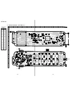
BASE RF BOARD
(COMPONENT SIDE)
BASE RF BOARD
(CONDUCTOR SIDE)
L351-357
(PRINTED COIL)
B
BASE MAIN
BOARD
MOD
TX
GND
LO
GND
IF
(11)
11
(11)
11
(SHIELD CASE)
1
3
6
4
A
BASE MAIN
BOARD
ANT
GND
VCC
LE
DATA
CLK
1-676-653-
1-676-653-
CLK
DATA
LE
VCC
GND
ANT
IF
GND
LO
GND
TX
MOD
05
L355
L356
L357
(SHIELD CASE)
L354
L353
L352
L351
L309
C349
C382
R359
R317
C342
R341
C343
C386
C326
C327
R322
C321
C346
C397
C311
C379
C380
C381
R398
R397
R399
L306
C335
R332
JC316
R320
C347
C345
C319
C305
C308
C340
C348
R305
C383
IC302
1
12
24
13
RT301
L350
PRINTED
COIL
(
(
C399
5-5.
PRINTED WIRING BOARD – BASE RF Section –
(Page 29)
(Page 29)
Summary of Contents for SPP-933 - 900mhz Cordless Telephone
Page 3: ... 3 SECTION 1 GENERAL This section is extracted from instruction manual ...
Page 4: ... 4 ...
Page 5: ... 5 ...
Page 6: ... 6 ...
Page 7: ... 7 ...
Page 8: ... 8 ...
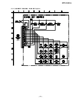
Page 27: ... 35 SPP 933 934 5 10 SCHEMATIC DIAGRAM BASE KEY Section Page 32 ...


